EP0665306A1 - Verfahren und Vorrichtung zum Zünden von Plasmen in einem Process modul - Google Patents
Verfahren und Vorrichtung zum Zünden von Plasmen in einem Process modul Download PDFInfo
- Publication number
- EP0665306A1 EP0665306A1 EP95100710A EP95100710A EP0665306A1 EP 0665306 A1 EP0665306 A1 EP 0665306A1 EP 95100710 A EP95100710 A EP 95100710A EP 95100710 A EP95100710 A EP 95100710A EP 0665306 A1 EP0665306 A1 EP 0665306A1
- Authority
- EP
- European Patent Office
- Prior art keywords
- gap
- gas
- module
- electrodes
- radiofrequency
- Prior art date
- Legal status (The legal status is an assumption and is not a legal conclusion. Google has not performed a legal analysis and makes no representation as to the accuracy of the status listed.)
- Granted
Links
Images


Classifications
-
- H—ELECTRICITY
- H01—ELECTRIC ELEMENTS
- H01J—ELECTRIC DISCHARGE TUBES OR DISCHARGE LAMPS
- H01J37/00—Discharge tubes with provision for introducing objects or material to be exposed to the discharge, e.g. for the purpose of examination or processing thereof
- H01J37/32—Gas-filled discharge tubes
- H01J37/32009—Arrangements for generation of plasma specially adapted for examination or treatment of objects, e.g. plasma sources
- H01J37/32082—Radio frequency generated discharge
-
- C—CHEMISTRY; METALLURGY
- C23—COATING METALLIC MATERIAL; COATING MATERIAL WITH METALLIC MATERIAL; CHEMICAL SURFACE TREATMENT; DIFFUSION TREATMENT OF METALLIC MATERIAL; COATING BY VACUUM EVAPORATION, BY SPUTTERING, BY ION IMPLANTATION OR BY CHEMICAL VAPOUR DEPOSITION, IN GENERAL; INHIBITING CORROSION OF METALLIC MATERIAL OR INCRUSTATION IN GENERAL
- C23C—COATING METALLIC MATERIAL; COATING MATERIAL WITH METALLIC MATERIAL; SURFACE TREATMENT OF METALLIC MATERIAL BY DIFFUSION INTO THE SURFACE, BY CHEMICAL CONVERSION OR SUBSTITUTION; COATING BY VACUUM EVAPORATION, BY SPUTTERING, BY ION IMPLANTATION OR BY CHEMICAL VAPOUR DEPOSITION, IN GENERAL
- C23C16/00—Chemical coating by decomposition of gaseous compounds, without leaving reaction products of surface material in the coating, i.e. chemical vapour deposition [CVD] processes
- C23C16/44—Chemical coating by decomposition of gaseous compounds, without leaving reaction products of surface material in the coating, i.e. chemical vapour deposition [CVD] processes characterised by the method of coating
- C23C16/50—Chemical coating by decomposition of gaseous compounds, without leaving reaction products of surface material in the coating, i.e. chemical vapour deposition [CVD] processes characterised by the method of coating using electric discharges
- C23C16/505—Chemical coating by decomposition of gaseous compounds, without leaving reaction products of surface material in the coating, i.e. chemical vapour deposition [CVD] processes characterised by the method of coating using electric discharges using radio frequency discharges
- C23C16/509—Chemical coating by decomposition of gaseous compounds, without leaving reaction products of surface material in the coating, i.e. chemical vapour deposition [CVD] processes characterised by the method of coating using electric discharges using radio frequency discharges using internal electrodes
- C23C16/5096—Flat-bed apparatus
-
- C—CHEMISTRY; METALLURGY
- C23—COATING METALLIC MATERIAL; COATING MATERIAL WITH METALLIC MATERIAL; CHEMICAL SURFACE TREATMENT; DIFFUSION TREATMENT OF METALLIC MATERIAL; COATING BY VACUUM EVAPORATION, BY SPUTTERING, BY ION IMPLANTATION OR BY CHEMICAL VAPOUR DEPOSITION, IN GENERAL; INHIBITING CORROSION OF METALLIC MATERIAL OR INCRUSTATION IN GENERAL
- C23C—COATING METALLIC MATERIAL; COATING MATERIAL WITH METALLIC MATERIAL; SURFACE TREATMENT OF METALLIC MATERIAL BY DIFFUSION INTO THE SURFACE, BY CHEMICAL CONVERSION OR SUBSTITUTION; COATING BY VACUUM EVAPORATION, BY SPUTTERING, BY ION IMPLANTATION OR BY CHEMICAL VAPOUR DEPOSITION, IN GENERAL
- C23C16/00—Chemical coating by decomposition of gaseous compounds, without leaving reaction products of surface material in the coating, i.e. chemical vapour deposition [CVD] processes
- C23C16/44—Chemical coating by decomposition of gaseous compounds, without leaving reaction products of surface material in the coating, i.e. chemical vapour deposition [CVD] processes characterised by the method of coating
- C23C16/50—Chemical coating by decomposition of gaseous compounds, without leaving reaction products of surface material in the coating, i.e. chemical vapour deposition [CVD] processes characterised by the method of coating using electric discharges
- C23C16/517—Chemical coating by decomposition of gaseous compounds, without leaving reaction products of surface material in the coating, i.e. chemical vapour deposition [CVD] processes characterised by the method of coating using electric discharges using a combination of discharges covered by two or more of groups C23C16/503 - C23C16/515
-
- H—ELECTRICITY
- H01—ELECTRIC ELEMENTS
- H01J—ELECTRIC DISCHARGE TUBES OR DISCHARGE LAMPS
- H01J37/00—Discharge tubes with provision for introducing objects or material to be exposed to the discharge, e.g. for the purpose of examination or processing thereof
- H01J37/32—Gas-filled discharge tubes
- H01J37/32009—Arrangements for generation of plasma specially adapted for examination or treatment of objects, e.g. plasma sources
- H01J37/32082—Radio frequency generated discharge
- H01J37/32137—Radio frequency generated discharge controlling of the discharge by modulation of energy
- H01J37/32155—Frequency modulation
- H01J37/32165—Plural frequencies
Definitions
- This invention relates to apparatus and methods for exposing samples to reactive plasmas. More particularly, the invention relates to apparatus and methods for igniting plasma within a process module that is, for example, suitable for use in Chemical Vapor Deposition (CVD) and in Plasma Enhanced Chemical Vapor Deposition (PECVD) processes.
- CVD Chemical Vapor Deposition
- PECVD Plasma Enhanced Chemical Vapor Deposition
- sample generically describes a substrate, such as a glass panel or a silicon wafer, which is suitable for deposition techniques, for example by PECVD.
- the sample typically has one surface that is treated to receive one or more film depositions.
- Vacuum deposition systems which deposit semiconducting or insulating films onto samples are well-known and are utilized in a wide range of scientific fields.
- Complex PECVD systems have been developed, for example, to manufacture devices such as thin film transistors (TFTs), liquid crystal displays (LCDs), flat panel displays (FPDs), solar cells, photodetectors, and integrated circuit structures.
- TFTs thin film transistors
- LCDs liquid crystal displays
- FPDs flat panel displays
- solar cells photodetectors
- integrated circuit structures integrated circuit structures
- these systems include one or more evacuated process modules that are used to expose the sample to reactive plasmas.
- a process module typically includes first and second electrodes within a chamber and spaced apart to form a gap therebetween: one electrode is electrically grounded to the chamber, and the other electrode is connected to a radiofrequency (RF) source which generates a radiofrequency discharge within the gap.
- RF radiofrequency
- the module also has gas inlets and gas outlets which direct selected gases, such as silane, into and through the gap.
- the sample is suspended in the gap spaced away from the active RF electrode, e.g., mounted to the grounded electrode, and a selected gas introduced into the inter-electrode gap.
- a selected gas introduced into the inter-electrode gap.
- the gas When the gas is exposed to the RF field, it ionizes and forms a reactive plasma which deposits a film onto surfaces exposed to the plasma, including the sample surface.
- the rate at which this film is deposited onto the sample surface is dependent upon several factors, including: the magnitude of the vacuum in the process module; the electrode spacing; the power and the frequency of the RF energy; and the gas flow rate.
- an object of the invention is to provide PECVD apparatus and methods which increase the deposition rate of films deposited on samples exposed to reactive plasmas.
- Another object of the invention is to provide vacuum deposition systems that expose samples to reactive plasmas, and which attain relatively high production yield.
- Further object of the invention is to provide such apparatus and methods for exposing samples to reactive plasma and which are relatively low in cost and reliable in operation.
- Yet another object of the invention is to provide apparatus and methods of the above character and which also can etch sample surfaces.
- the invention attains the aforementioned objectives by providing, in one aspect, improvements to plasma process modules which expose samples to reactive plasma.
- These modules include first and second radiofrequency electrodes and a radiofrequency generator connected to the second electrode.
- the first and second electrodes are spaced apart to form a substantially uniform gap therebetween of less than approximately one centimeter.
- the improvement also features an ionizing element for ionizing gas injected between the electrodes.
- the ionizing element ignites the plasma within the electrode gap and the radiofrequency energy generator afterwards transforms molecules within the module into plasma by generating RF energy at a primary frequency that is preferably sixty megahertz.
- the improvement preferably comprises a gas that is injected between the electrodes.
- the gas is of a type that is suitable for ionization and that is suitable for transformation into a plasma when exposed to radiofrequency energy at the primary frequency.
- the gas is generally selected from gases such as silane (SiH4), disilane (Si2H6), hydrogen (H2), ammonia (NH3), phosphine (PH3), nitrogen (N2), nitrogen trifluoride (NF3), helium (He), argon (Ar), carbon tetrafluoride (CF4), hexafluoroethane (C2F6), oxygen (O2), nitrous oxide (N2O), methane (CH4), borane (BH3), diborane (B2H6), chlorine (Cl2), sulfur hexafluoride (SF6), hydrogen chloride (HCl), carbon tetrachloride (CCl4), hydrogen bromide (HBr), carbon dichloride difluoride (
- the improvements thus include, in other aspects, gas inlets and gas outlets, and associated pump mechanisms.
- the pump mechanisms pump gas through the gas inlet and into the gap, and extract gas and other molecules through the gas outlet as process waste.
- the invention provides an electron source with a filament as the ionizing element.
- the electron source is arranged to inject electrons between the electrodes at an energy that is preferably at least 300eV to ionize gas in the gap.
- the electron source is spaced selectively at a distance from the gap to select the electron energy entering the gap.
- the source includes an extraction slit that has a selectively variable positive potential relative to the filament, for extracting electrons from the filament with energies of variable magnitude and greater than 300eV.
- the improvement provides an ultraviolet light source as the ionizing element and which irradiates ultraviolet radiation between the electrodes to ionize gas in the gap.
- the ultraviolet light source preferably generates photons with energies that are greater than approximately five electron volts.
- the improvement includes an UV interface that is transmissive to the ultraviolet radiation generated by the UV source, so that the UV source generates photons which irradiate the gap through the UV interface.
- Such an ultraviolet light source is preferably located in standard atmosphere outside the module, which is evacuated, and is arranged to illuminate the vacuum of the evacuated module through the UV interface.
- the ultraviolet light source includes (i) a reflector and an aperture which, in combination, collect the emitted ultraviolet radiation and transmit the radiation in a concentrated direction toward the gap in the module; and (ii) one or more optical elements which collect and collimate the transmitted concentrated radiation from the reflector to the within the gap.
- the improvement provides a sparking apparatus as the ionizing element.
- the sparking apparatus generates a spark or other electric discharge between the electrodes to ionize gas in the gap.
- the sparking apparatus is isolated from the ground of the process chamber and has an exposed spark gap arranged with a line of sight from the spark gap to between the electrodes, such that an emitted spark at the spark gap injects electrons to within the gap.
- the improvement provides a second radiofrequency generator that is connected to the second electrode.
- the second radiofrequency generator has a second frequency, preferably 400kHz, that is less than the primary frequency and that generates radiofrequency discharges between the electrodes at the second frequency to ionize gas in the gap.
- the second radiofrequency generator pulses the second frequency at a selected rate. It is also preferred, according to the invention, to inhibit the second radiofrequency generator once gas is ionized within the gap.
- the two radiofrequency generators typically operate in combination to generate a voltage between approximately 1kV and 5kV across the two electrodes.
- a process module includes a high direct current power source that is connected to the second electrode.
- a direct current power source generates a physical spark between the electrodes and accordingly ionizes gas in the gap.
- a process module of the invention includes evacuation apparatus, e.g., a pump and/or compressor, that evacuates the module selectively to approximately 0.01 Torr (0.0133 mbar).
- evacuation apparatus e.g., a pump and/or compressor
- pressurizing apparatus e.g., a pump and/or compressor
- the improvement provides for alternately controlling the pressure within the module to selectively pressurize the module for a short duration within which ionization of gas occurs. For example, the module is first evacuated by a pump to approximately .01 Torr (0.0133 mbar) so that oxidation and sample impurity is kept to a minimum.
- a deposition or etch gas is injected between the electrodes and the pump pressurizes the module to approximately .5 Torr (0.665 mbar) so that the gas is ignited by the primary frequency generator. Once gas is ionized, the module is depressurized to approximately .1 Torr (0.133 mbar) which is a preferred deposition or etch operational pressure.
- the process module of the invention includes an x-ray source, or alternatively a radioactive source, as the ionization element.
- the x-ray or radioactive source is arranged to generate a beam of x-ray or radioactive radiation into the gap to ionize gas therein.
- a source is shielded to confine the x-ray or radioactive radiation substantially to one or more paths extending from the source and through the gap.
- a first primary gas can include silane (SiH4), disilane (Si2H6), hydrogen (H2), ammonia (NH3), phosphine (PH3), nitrogen trifluoride (NF3), helium (He), carbon tetrafluoride (CF4), hexafluoroethane (C2F6), oxygen (O2), nitrous oxide (N2O), methane (CH4), borane (BH3), diborane (B2H6), chlorine (Cl2), sulfur hexafluoride (SF6), hydrogen chloride (HCl), carbon tetrachloride (CCl4), hydrogen bromide (HBr), carbon dichloride difluoride (CCl2F2), boron trichloride (BCl3), silicon tetrachloride (SiCl4), boron tribromide (
- a second gas such as helium (He), argon (Ar), krypton (Kr), nitrogen (N2), xenon (Xe) neon (Ne), and mixtures thereof, is combined with the first gas to form a gaseous mixture that is transformable into plasma by the primary frequency.
- the mixture of the two gases is ignitable by a radiofrequency source that generates 60MHz discharges. Once the mixture of the two gases is ignited, the second gas is inhibited from flowing into the module so that deposition onto a sample surface results without influence from the second gas.
- the improvement of the invention includes a motion actuator, e.g., a linear actuator, as the ionization element and which moves at least one of the electrodes selectively to change the dimension of the gap between the electrodes.
- the motion actuator separates the electrodes to a first dimension, at which the radiofrequency generator, of high primary frequency, ionizes gas injected between the electrodes.
- the motion actuator thereafter reduces the gap spacing to below approximately one centimeter, a desired dimension for high rate plasma deposition.
- the improvement includes an atomic element as the ionization element and which has an ionization energy of no more than twenty-five electron volts.
- the atomic element such as helium or argon, is injected into the gap to ionize gas therein.
- the invention also provides a sample-processing method for exposing a sample to reactive plasma within a process module having first and second electrodes.
- the improvement includes the steps of (i) arranging the first and second electrodes within the module to form a substantially uniform gap separating the electrodes of between approximately one and ten millimeters; (ii) injecting a gas, such as silane (SiH4), disilane (Si2H6), hydrogen (H2), ammonia (NH3), phosphine (PH3), nitrogen (N2), nitrogen trifluoride (NF3), helium (He), argon (Ar), carbon tetrafluoride (CF4), carbon tetrachloride (CCl4), hexafluoroethane (C2F6), oxygen (O2), nitrous oxide (N2O), methane (CH4), borane (BH3), diborane (B2H6), and mixtures thereof, into the gap; (iii) ionizing the
- the method includes the step of injecting a second gas into the gap wherein the first and second gases form a gaseous mixture that is transformable into plasma by the primary frequency.
- the second gas is helium (He), argon (Ar), krypton (Kr), nitrogen (N2), xenon (Xe) neon (Ne), or mixtures thereof.
- the method according the invention includes the additional steps of (i) injecting into the module an etch gas, such as chlorine (Cl2), sulfur hexafluoride (SF6), hydrogen chloride (HCl), carbon tetrachloride (CCl4), hydrogen bromide (HBr), carbon tetrafluoride (CF4), hexafluoroethane (C2F6), nitrogen trifluoride (NF3), carbon dichloride difluoride (CCl2F2), boron trichloride (BCl3), silicon tetrachloride (SiCl4), oxygen (O2), boron tribromide (BBr3), chlorotrifluoride (ClF3), fluorine (F2), or mixtures thereof; (ii) ionizing the etch gas; and (iii) applying to the gap radiofrequency energy with a primary frequency, e.g., 60MHz, to transform the etch gas into an etch plasma such that surfaces in contact with a primary frequency
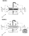
- Fig. 1 schematically illustrates a process module 10a constructed in accordance with the invention.
- the module 10a includes a first radiofrequency (RF) electrode 12, a second RF electrode 14, and a RF generator 16 interconnected with the second electrode 14.
- the electrodes are spaced apart at a distance "d” to form a substantially uniform gap 18 between the electrodes 12 and 14.
- the distance "d” is less than approximately ten millimeters and preferably more than one millimeter.
- a pressure-tight housing 20 surrounds the electrodes 12 and 14 so that the module 10a may be evacuated selectively, to between approximately 0.01 and ten Torr (0.0133 and 13.3 mbar), by methods known to those skilled in the art.
- the module 10a includes gas inlet 24 and gas outlet 26: the inlet 24 is used to inject gas into the module 10a; and the outlet 26 is used to extract gas, particulates, and other molecules from the module 10a.
- a gas that is suitable for ionization and for transformation into plasma e.g., silane
- the gas is ionized, in accordance with further features of the invention described below, and transformed into plasma by RF energy, which preferably has a primary frequency of 60MHz.
- the RF energy is generated by the generator 16 and transferred to the gap 18 via the RF connection 28 and electrodes 12 and 14, thereby transforming molecules of the injected gas into a plasma 30.
- a film is deposited onto surfaces in contact with the plasma 30.
- a sample 32 e.g., a flat glass or silicon wafer with opposed surfaces, is introduced into the gap 18 in the module 10a to expose the sample 32 to the plasma 30 for deposition of one or more films onto its surface.
- the sample 32 is typically mounted to the first electrode 12 such that the sample 32 is spaced away from the active RF second electrode 14.
- the first electrode 12, therefore, is preferably electrically grounded by the grounding connection 34 and ground 36.
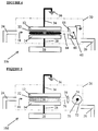
- Fig. 2, 4, 5, 5A, 6, 7, and 8 illustrate similar pressure modules 10 constructed according to the invention, and which show other preferred features of the invention.
- These figures show the sensing modules 10 in schematic cross-sectional views; yet it is to be understood that such views are to be interpreted in the context of a three-dimensional structure.
- the modules 10 of Fig. 1, 2, 4, 5, 5A, 6, 7 and 8 are generally rectangular in shape, each having another cross-sectional view that is similar in size, and perpendicular to, the associated illustrated view.
- Further understanding of a three-dimensional process module may be made with reference to Fig. 2, of U.S. Application Serial No. 08/084415, entitled "Method and Apparatus for Inverting Samples in a Process", which is incorporated herein by reference.
- Fig. 2 illustrates the module 10b connected to a pressure pump 42 at the gas outlet 26; and further including linear actuators 44 connected to the first electrode 12.
- Either of the structures 42 and 44 are independently operable in conjunction with other elements of the module 10b to ignite gas within the gap 18; or, alternatively, they cooperate together with the other elements of the module 10 to ignite the gas.
- Fig. 3 qualitatively illustrates plasma maintenance curves for two typical gases, Gas 1 and Gas 2, as the relation between the voltage differential required between the electrodes to maintain a discharge and the product of pressure and electrode spacing.
- the product of pressure and electrode spacing represents the horizontal axis.
- the voltage differential required between the electrodes to maintain a discharge within the gap 18 represents the vertical axis.
- Gas 1 and Gas 2 The shape of these two plasma maintenance curves, Gas 1 and Gas 2, can be understood with reference to the ionization physics within the module 10b.
- electrons To ignite and maintain a plasma within the module 10b, electrons must be accelerated within the gap 18 to energies in which the collisions of the accelerated electrons with the gas molecules in the gap 18 cause ionization of the gas molecules, i.e., the creation of more electrons and ions.
- the probability for an electron to cause ionization is directly proportional to the pressure within the module 10b and the distance traveled by the electron in the plasma, as controlled by the electrode spacing.
- the preferred operating conditions for depositing film from typical Gas 1 occur in region A, Fig. 3.
- a plasma of hydrogen and silane is ignited in one instance at pressures above 0.6 Torr (0.8 mbar); however, below that pressure, no plasma is ignited. Nevertheless, after ignition at 0.6 Torr (0.8 mbar), the pressure is reduced to as low as 0.1 Torr (0.133 mbar), since the required voltage to maintain a discharge, and hence maintain the plasma, is lower than the voltage required to ignite, and thereby initiate, the plasma.
- the minimum plasma maintenance voltage for Gas 1, i.e. Vmin, relative to the pressure-electrode product, i.e. (pd)min, is gas dependent.
- the electrode spacing and/or module pressure are modified as a function of the particular gas within the module 18 to enable ignition, i.e., the transformation of those gas molecules into the plasma 30.
- deposition gases gases are generally classified into two groups: deposition gases and etch gases.
- the preferred deposition gases used in accordance with the invention are silane (SiH4), disilane (Si2H6), hydrogen (H2), ammonia (NH3), phosphine (PH3), nitrogen (N2), nitrogen trifluoride (NF3), helium (He), argon (Ar), carbon tetrafluoride (CF4), hexafluoroethane (C2F6), oxygen (O2), nitrous oxide (N2O), methane (CH4), borane (BH3), diborane (B2H6), and mixtures thereof (the preferred deposition mixtures are silane and hydrogen; silane, ammonia and nitrogen; silane and phosphine; silane and methane; silane and borane; and silane and diborane).
- the preferred etch gases used in accordance with the invention are chlorine (Cl2), sulfur hexafluoride (SF6), hydrogen chloride (HCl), carbon tetrafluoride (CF4), hydrogen bromide (HBr), carbon tetrachloride (CCl4), nitrogen trifluoride (NF3), carbon dichloride difluoride (CCl2F2), boron trichloride (BCl3), silicon tetrachloride (SiCl4), oxygen (O2), boron tribromide (BBr3), chlorotrifluoride (ClF3), fluorine (F2), and mixtures thereof (the preferred etch mixtures are carbon tetrafluoride and oxygen; hexafluoride and oxygen; and nitrogen trifluoride and oxygen).
- the RF generator 16 With an electrode spacing of less than approximately ten millimeters, the RF generator 16 generally does not provide sufficient voltage to transform gas molecules injected into the gap 18 into plasma, such as illustrated in region A of Fig. 3.
- the pressure pump 42 of Fig. 2 initially operates as a vacuum pump to evacuate the module 10b to approximately 0.01 Torr (0.0133 mbar), which reduces oxidation and other impurities that might form on the heated samples. Selected deposition gas molecules are then injected into the module 10b, and the pressure pump 42 controls the pressure within the module 10b by operation of the throttle 41 to between approximately 0.1 to 1 Torr (0.133 to 1.33 mbar), which represents a pressure range that permits ionization of the gas molecules by the primary RF generator 16.
- the throttle 41 functions as an orifice within the gas outlet 26 to increase or decrease the pressure in the module selectively: decreasing the orifice of the throttle 41 increases the pressure within the module 10b; while increasing the orifice decreases the module pressure.
- the pressure pump 42 increases the pressure within the module 10b selectively, such as in accordance with the plasma maintenance curve of Fig. 3, as a function of the gas within the module to enable the transformation of the gas molecules into plasma. Once the plasma is ignited, the pump 42 evacuates, or de-pressurizes, the module 10 to normal pressures, e. g., .1 Torr (0.133 mbar), which are preferred for uniform high rate deposition.
- the pressure pump 42 of Fig. 2 is selectively operable to (i) pressurize the module 10b to enable the transformation of gas molecules injected into the gap 18 into plasma and (ii) de-pressurize, e.g., evacuate, the module 10b to enable high rate deposition at preferred conditions.
- the pump 42 is readily constructed as a vacuum pump or combination pump and compressor to provide the operations (i) and (ii).
- the operation between pressurization and depressurization within the module 10b is controllable, in accordance with the invention; and preferably short in duration, e.g., 1 second, so that gas is ionized and the module 10b returns to normal evacuated pressures without lengthy pressurization of the module 10b.
- a similar ignition procedure is realized through operation of the linear actuators 44.
- the actuators 44 are connected to the first electrode 12 to move the electrode 12 and adjust the gap separation "d" selectively.
- the actuators 44 increase the separation between the electrodes 12 and 14 to a point, for example in accordance with Fig. 3, where the RF generator ignites and transforms the molecules into the plasma 30.
- the RF generator 16 has sufficient voltage to maintain the plasma 30 within the gap 18; thus the actuators 44 reposition the electrode 12 to a gap separation "d" of less than approximately one centimeter to increase the deposition rate.
- Linear actuators 44 preferably reside within the housing 22 so that the module 10b is evacuated without required mechanical motion through the sealed module housing wall 20. Therefore, the actuators 44 have electrical components (not shown), including wires and electrical feed-through fittings, which extend from the actuators 44 and through the housing 20 for communication to outside of the module 10. Alternatively, although not preferred, the actuators 44 physically extend through the evacuated module housing 20 through the use of mechanical seals (not shown).
- the pump 42 and the actuators 44 preferably operate simultaneously with the RF generator 16 to ionize gas.
- the required voltage to transform molecules into plasma decreases more rapidly by simultaneously increasing module pressure and electrode spacing. Therefore, the undesirable time duration away from ideal deposition conditions, e.g., .1 Torr (0.133 mbar) and 1-9mm gap separation, is decreased.
- the invention thus provides the pump 42 and the actuators 44 to aid in the ionization of gas injected between the electrodes.
- the generator 16 cannot generally ionize gas at low pressures, e.g., 0.1 Torr (0.133 mbar), and at small gap separations, e.g., 1-9mm, without the further features of the invention, e.g., the pump 42, the actuators 44, and other practices according to the invention taught below.
- the module 10b has a total fixed capacitance that is dependent, in part, upon the module geometry, e.g., the electrode gap spacing.
- the total fixed module capacitance has a relatively low associated impedance. This translates to a low voltage differential between the electrodes 12 and 14 for a given power. For ignition purposes, only voltage is important; hence the requirement for additional features according to the invention, such as the pump 42 and actuators 44.
- Fig. 4 shows a module 10c with the addition of an electron source 60, in accordance with the invention.
- the electron source 60 has a hot filament 62, operating at a low voltage and at approximately 10 amps, and emits a beam of electrons 64 through an extraction slit 66 and into the gap 18.
- the slit 66 is approximately ten millimeters in length and one millimeter in height, and is parallel to the gap 18.
- the filament 62 is at a negative potential relative to the grounded extraction slit 66 to "extract" the electrons from the filament 62 surface. Accordingly, gas injected into the gap 18 is ionized at a selective time by applying a positive voltage to the slit 66 once the filament 62 is emitting electrons.
- the electrons 64 emitted by the filament 62 have energies of approximately 300eV when the filament is positioned at approximately 70mm or less from the gap 18. If the filament 62 is positioned nearer to the gap 18, less energy is acceptable. However, if the filament 62 is positioned further from the gap 18, more energy is required. This phenomenon occurs because the emitted electrons 64 lose energy during travel to the gap 18, such as through collisions with other molecules in the module 10c. Additionally, different gases within the module 10c require different ionization energies. Therefore, the invention provides for differing electron illumination energies by changing the negative potential of the filament 62. This potential is adjusted by changing the voltage between the filament 62 and slit 66 to alter the energy of the emitted electrons.
- electron sources exist which are manufactured without the filament 62 of Fig. 4, and which are suitable for igniting the gas within the gap 18.
- the probability of ionizing gas within the gap 18 is at a maximum when electrons with energies between approximately 50eV and 100eV collide with the gas molecules in the gap 18. Therefore, other electron sources which are operable to generate electrons with energies between approximately 50eV as 100eV within the gap 18 are also suitable for ionizing gas therein in accord with the invention.
- Fig. 5 and 5A illustrate one preferred practice of the invention in which an ultraviolet (UV) source 70, 72 illuminates and ignites gas within the gap 18 with UV photons:
- Fig. 5 shows the UV source 70, 72 within the evacuated module 10d; while
- Fig. 5A shows the UV source 70, 72 outside the module 10e, in standard atmosphere.
- UV ultraviolet
- Fig. 5 illustrates the module 10d with a UV lamp 70 that emits UV photons.
- a reflector 72 surrounds the lamp 70 such that emitted photons are collected and are emitted only through the aperture 74, which directs the UV photon beam 76 generally towards the gap 18.
- the beam 76 is substantially collected and collimated by UV transmitting optics 78 such that the beam 76 illuminates the gap 18 without significant loss of intensity.
- Fig. 5A shows a UV source 70, reflector 72, aperture 74, beam 76, and optics 78, and additionally shows an optical interface 79 that transmits UV radiation and which preferably withstands operational pressure differentials.
- the interface 79 is required because the UV source 70 of Fig. 5A is positioned outside the process module 10e, e.g., exterior to the pressure-sealing housing 20'. UV energy cannot transmit through materials which typically form the housing 20', e.g. aluminum, and thus a glass-like interface 79 is required.
- the photon energies emitted by the UV source 70, 72 of Fig. 5 and 5A are greater than approximately five electron volts.
- Fig. 6 shows another preferred practice of the invention in which a sparking source 80 generates a spark to ignite the gas within the gap 18.
- the sparking source has a power supply 82 connected to a spark gap 84, and is preferably electrically isolated from the electrodes 12 and 14.
- the power supply 82 applies a voltage across the gap 84 selectively to generate a spark.
- the sparking source is arranged within the module 10f such that generated sparks are introduced into the gap 18, thus ionizing gas therein.
- the gap 84 has a line of sight 86 directly to the gap 18.
- a spark is generally induced by a voltage differential across the gap 84 in the kilovolt range and thus generates electrons with high energies.
- These electrons emit in all directions and many collide with the electrodes 12 and 14, which in turn release secondary electrons that ignite the gas within the gap 18.
- These secondary electrons include electrons with maximum ionization probabilities for a given gas, e.g., those electrons with energies between approximately 50eV and 100eV.
- Fig. 7 shows another preferred practice of the invention for igniting gas within a process module 10g.
- the process module 10g has a second RF generator 90 connected to the second electrode 14 via RF line 92.
- the second RF generator 90 has a second frequency, preferably 400kHz, which is less than the preferred primary frequency of 60MHz.
- the second RF generator 90 is selectively operable to apply RF energy at the lower frequency to the gap 18.
- the second RF generator 90 is energized only for a short duration, at a time sufficient to ionize gas within the gap 18. Alternatively, the generator 90 is repetitively pulsed at approximately once per second to ionize the gas.
- the primary 60MHz energy combines with the lower 400kHz energy to ignite and ionize the gas.
- Each generator 16 and 90 provides approximately equal energy, e.g., .05W/cm2 to 1W/cm2 within the gap 18; yet, as stated earlier, the high frequency of the first RF generator 16 lacks sufficient voltage to ionize gas within a gap 18 spaced at less than approximately one centimeter.
- the lower frequency generator 90 provides relatively high voltage across the electrodes.
- the module capacitance has a much higher associated impedance and greater peak-to-peak voltage as compared to a 60MHz frequency.
- a high voltage generates high electron energies with a corresponding increase in ionization probability. Accordingly, the generators 90 and 16 preferably combine to generate a peak-to-peak voltage between approximately one kilovolt and five kilovolts in the gap 18.
- the second RF generator 90 is that, unlike other ignition techniques described herein, no internal modifications to the module 10 are needed to ignite the gas.
- the generator 90 is external to the housing 20 and connects with the second electrode 14 through the RF line 92.
- the line 92 is coaxial with the RF line 28, to reduce the required cabling, which pierces the evacuated housing 20 at a pressure-tight RF feed-through fitting.
- the generator 90 is not an RF generator; but is instead a high DC power source.
- voltage is an important ionization parameter.
- DC source 90 in this alternative embodiment, generates a spark in the gap selectively to ionize gas therein.
- the DC source 90 combines with the 60MHz energy to ignite and ionize the gas. After the gas is ionized and molecules have been transformed into plasma, the DC power source 90 is turned off.
- Fig. 8 shows a process module 10h constructed according to a further practice of the invention and which includes an x-ray source 100 and shielding 102.
- the x-ray source 100 and shielding 102 are constructed by methods known in the art to generate a beam of x-ray radiation 104 that extends through at least part of the gap 18.
- the x-ray source 100 is preferably embedded within one of the electrodes 12 and 14', here shown imbedded in electrode 14'.
- the shielding 102 confines the x-ray radiation to the desired beam 104, and thereby protects users of the process module 10h from the unwanted x-rays.
- the source 100 can be a radioactive source in accordance with the invention.
- a shielding 102 protects users of the module 10 and guides the emitted radioactive particles along a path that includes the gap 18.
- X-ray and other radioactive radiation provide the energy required to ionize gases within the gap 18.
- the source 100 is preferably covered, via an automatic mechanical shutter (not shown), since the RF generator 16 has sufficient power to maintain plasma once the gas is ionized.
- the source 100 may be positioned elsewhere to ionize gas within the gap 18. However, it is a convenient packaging to locate the source 100 within one of the electrodes 12 and 14', since both x-rays and radioactive energy propagate through the electrode material.
- the inlet 24 is used in one practice of the invention to inject combinations of gases, rather than a single gas for ionization.
- a second inlet 24 is installed into the housing wall 20 to inject additional gases. These additional gases can act as the catalyst to ignite the primary gas from which the plasma 30 is derived. More particularly, by injecting a second gas comprising helium, xenon, krypton, nitrogen, argon, neon, or other atomic elements with a primary gas, e.g., silane, electrons liberated by ionization of the molecules of the second gas cause further ionization of the primary gas molecules, e.g., silane, and enable the transformation of molecules into a plasma.
- a primary gas e.g., silane
- these second gases are injected for a short duration through the inlet 24 until the gas combination ignites, whereinafter the second gas is inhibited from flowing through the module so that a deposition from a "pure", e.g., silane-based plasma results.
- the injected atomic elements have ionization energies which are less than approximately 25eV.
- Etch gases such as chlorine (Cl2), sulfur hexafluoride (SF6), hydrogen chloride (HCl), nitrogen trifluoride (NF3), carbon tetrachloride (CCl4), hydrogen bromide (HBr), carbon tetrafluoride (CF4), carbon dichloride difluoride (CCl2F2), boron trichloride (BCl3), silicon tetrachloride (SiCl4), boron tribromide (BBr3), chlorotrifluoride (ClF3), and fluorine (F2) are typically mixed with oxygen (O2) to form the preferred gaseous mixture that is ignited according to the further features of the invention.
- the electrode spacing is generally spaced to between approximately one and seventy five millimeters.
- Appendix A are detailed drawings and assembly documents that present further details of preferred constructions of process modules that (i) ignite gas and (ii) expose samples to plasma, in accordance with the invention.
Landscapes
- Chemical & Material Sciences (AREA)
- Engineering & Computer Science (AREA)
- Physics & Mathematics (AREA)
- Plasma & Fusion (AREA)
- Mechanical Engineering (AREA)
- General Chemical & Material Sciences (AREA)
- Chemical Kinetics & Catalysis (AREA)
- Materials Engineering (AREA)
- Analytical Chemistry (AREA)
- Metallurgy (AREA)
- Organic Chemistry (AREA)
- Plasma Technology (AREA)
- Physical Vapour Deposition (AREA)
- Chemical Vapour Deposition (AREA)
- ing And Chemical Polishing (AREA)
- Measurement Of The Respiration, Hearing Ability, Form, And Blood Characteristics Of Living Organisms (AREA)
- Electron Sources, Ion Sources (AREA)
Applications Claiming Priority (2)
| Application Number | Priority Date | Filing Date | Title |
|---|---|---|---|
| US183529 | 1994-01-19 | ||
| US08/183,529 US5565036A (en) | 1994-01-19 | 1994-01-19 | Apparatus and method for igniting plasma in a process module |
Publications (2)
| Publication Number | Publication Date |
|---|---|
| EP0665306A1 true EP0665306A1 (de) | 1995-08-02 |
| EP0665306B1 EP0665306B1 (de) | 2001-10-31 |
Family
ID=22673192
Family Applications (1)
| Application Number | Title | Priority Date | Filing Date |
|---|---|---|---|
| EP95100710A Expired - Lifetime EP0665306B1 (de) | 1994-01-19 | 1995-01-19 | Verfahren und Vorrichtung zum Zünden von Plasmen in einem Process modul |
Country Status (5)
| Country | Link |
|---|---|
| US (2) | US5565036A (de) |
| EP (1) | EP0665306B1 (de) |
| JP (1) | JP3158236B2 (de) |
| AT (1) | ATE207978T1 (de) |
| DE (1) | DE69523488T2 (de) |
Cited By (19)
| Publication number | Priority date | Publication date | Assignee | Title |
|---|---|---|---|---|
| EP0880161A1 (de) * | 1997-05-20 | 1998-11-25 | Applied Materials, Inc. | Elektronenquelle zur Neutralisation von Aufladungen eines Substrats während einer Ionenimplantation |
| WO1999019537A1 (en) * | 1997-10-09 | 1999-04-22 | Applied Komatsu Technology, Inc. | Dual frequency excitation of plasma for film deposition |
| WO2000079018A1 (en) * | 1999-06-22 | 2000-12-28 | Tokyo Electron Limited | Sputtering method using virtual shutter |
| EP1198610A1 (de) * | 1999-05-14 | 2002-04-24 | The Regents of the University of California | Plasmastromerzeugungsvorrichtung mit weitem druckbereich bei niedrigen temperaturen |
| US6902683B1 (en) | 1996-03-01 | 2005-06-07 | Hitachi, Ltd. | Plasma processing apparatus and plasma processing method |
| NL1026532C2 (nl) * | 2004-06-30 | 2006-01-02 | Tno | Methode en middelen voor generatie van een plasma bij atmosferische druk. |
| US7329608B2 (en) | 1999-05-14 | 2008-02-12 | The Regents Of The University Of California | Method of processing a substrate |
| US11476145B2 (en) | 2018-11-20 | 2022-10-18 | Applied Materials, Inc. | Automatic ESC bias compensation when using pulsed DC bias |
| US11699572B2 (en) | 2019-01-22 | 2023-07-11 | Applied Materials, Inc. | Feedback loop for controlling a pulsed voltage waveform |
| US11791138B2 (en) | 2021-05-12 | 2023-10-17 | Applied Materials, Inc. | Automatic electrostatic chuck bias compensation during plasma processing |
| US11798790B2 (en) | 2020-11-16 | 2023-10-24 | Applied Materials, Inc. | Apparatus and methods for controlling ion energy distribution |
| US11848176B2 (en) | 2020-07-31 | 2023-12-19 | Applied Materials, Inc. | Plasma processing using pulsed-voltage and radio-frequency power |
| US11887813B2 (en) | 2021-06-23 | 2024-01-30 | Applied Materials, Inc. | Pulsed voltage source for plasma processing |
| US11901157B2 (en) | 2020-11-16 | 2024-02-13 | Applied Materials, Inc. | Apparatus and methods for controlling ion energy distribution |
| US11948780B2 (en) | 2021-05-12 | 2024-04-02 | Applied Materials, Inc. | Automatic electrostatic chuck bias compensation during plasma processing |
| US11967483B2 (en) | 2021-06-02 | 2024-04-23 | Applied Materials, Inc. | Plasma excitation with ion energy control |
| US11972924B2 (en) | 2022-06-08 | 2024-04-30 | Applied Materials, Inc. | Pulsed voltage source for plasma processing applications |
| US12106938B2 (en) | 2021-09-14 | 2024-10-01 | Applied Materials, Inc. | Distortion current mitigation in a radio frequency plasma processing chamber |
| US12125673B2 (en) | 2023-11-13 | 2024-10-22 | Applied Materials, Inc. | Pulsed voltage source for plasma processing applications |
Families Citing this family (77)
| Publication number | Priority date | Publication date | Assignee | Title |
|---|---|---|---|---|
| US6127277A (en) * | 1996-07-03 | 2000-10-03 | Tegal Corporation | Method and apparatus for etching a semiconductor wafer with features having vertical sidewalls |
| EP0925605A4 (de) * | 1996-07-03 | 2003-11-05 | Tegal Corp | Verfahren und anordnung zur ätzung von halbleiterscheiben |
| US6048435A (en) | 1996-07-03 | 2000-04-11 | Tegal Corporation | Plasma etch reactor and method for emerging films |
| US6500314B1 (en) | 1996-07-03 | 2002-12-31 | Tegal Corporation | Plasma etch reactor and method |
| US5911832A (en) * | 1996-10-10 | 1999-06-15 | Eaton Corporation | Plasma immersion implantation with pulsed anode |
| EP0865079A3 (de) | 1997-03-13 | 1999-10-20 | Applied Materials, Inc. | Verfahren zur Beseitigung von auf geätzten Platinflächen abgelagerten Verunreinigungen |
| JPH10340857A (ja) * | 1997-06-10 | 1998-12-22 | Mitsubishi Electric Corp | 半導体装置の製造方法及び半導体製造装置 |
| US8779322B2 (en) | 1997-06-26 | 2014-07-15 | Mks Instruments Inc. | Method and apparatus for processing metal bearing gases |
| US6388226B1 (en) | 1997-06-26 | 2002-05-14 | Applied Science And Technology, Inc. | Toroidal low-field reactive gas source |
| US7569790B2 (en) | 1997-06-26 | 2009-08-04 | Mks Instruments, Inc. | Method and apparatus for processing metal bearing gases |
| US6150628A (en) * | 1997-06-26 | 2000-11-21 | Applied Science And Technology, Inc. | Toroidal low-field reactive gas source |
| US6815633B1 (en) | 1997-06-26 | 2004-11-09 | Applied Science & Technology, Inc. | Inductively-coupled toroidal plasma source |
| JPH1187247A (ja) * | 1997-09-02 | 1999-03-30 | Matsushita Electron Corp | 半導体装置の製造装置及びその製造方法 |
| US6039849A (en) * | 1997-10-28 | 2000-03-21 | Motorola, Inc. | Method for the manufacture of electronic components |
| US6919168B2 (en) | 1998-01-13 | 2005-07-19 | Applied Materials, Inc. | Masking methods and etching sequences for patterning electrodes of high density RAM capacitors |
| US6265318B1 (en) | 1998-01-13 | 2001-07-24 | Applied Materials, Inc. | Iridium etchant methods for anisotropic profile |
| EP1048064A1 (de) | 1998-01-13 | 2000-11-02 | Applied Materials, Inc. | Ätzmethoden für anisotropes platin-ätzprofil |
| US6323132B1 (en) | 1998-01-13 | 2001-11-27 | Applied Materials, Inc. | Etching methods for anisotropic platinum profile |
| US6551939B2 (en) * | 1998-03-17 | 2003-04-22 | Anneal Corporation | Plasma surface treatment method and resulting device |
| US6149829A (en) | 1998-03-17 | 2000-11-21 | James W. Mitzel | Plasma surface treatment method and resulting device |
| US6235213B1 (en) * | 1998-05-18 | 2001-05-22 | Micron Technology, Inc. | Etching methods, methods of removing portions of material, and methods of forming silicon nitride spacers |
| US6187133B1 (en) * | 1998-05-29 | 2001-02-13 | Applied Materials, Inc. | Gas manifold for uniform gas distribution and photochemistry |
| US6277759B1 (en) * | 1998-08-27 | 2001-08-21 | Micron Technology, Inc. | Plasma etching methods |
| JP4180706B2 (ja) * | 1998-09-24 | 2008-11-12 | 和夫 寺嶋 | 物質・材料プロセッシング方法 |
| JP2000348896A (ja) * | 1999-03-26 | 2000-12-15 | Canon Inc | プラズマ発生方法、プラズマ発生装置及びプラズマ反応によるガス処理方法 |
| US6228438B1 (en) * | 1999-08-10 | 2001-05-08 | Unakis Balzers Aktiengesellschaft | Plasma reactor for the treatment of large size substrates |
| JP4221847B2 (ja) * | 1999-10-25 | 2009-02-12 | パナソニック電工株式会社 | プラズマ処理装置及びプラズマ点灯方法 |
| JP2004527727A (ja) * | 2000-07-05 | 2004-09-09 | シーアールティ ホールディングス、インク | 電磁気放射起動プラズマ反応炉 |
| US20020121500A1 (en) * | 2000-12-22 | 2002-09-05 | Rao Annapragada | Method of etching with NH3 and fluorine chemistries |
| JP3758520B2 (ja) * | 2001-04-26 | 2006-03-22 | 日新イオン機器株式会社 | イオンビーム照射装置および関連の方法 |
| US6673106B2 (en) * | 2001-06-14 | 2004-01-06 | Cordis Neurovascular, Inc. | Intravascular stent device |
| US20030013314A1 (en) * | 2001-07-06 | 2003-01-16 | Chentsau Ying | Method of reducing particulates in a plasma etch chamber during a metal etch process |
| JP4137419B2 (ja) * | 2001-09-28 | 2008-08-20 | 東京エレクトロン株式会社 | プラズマ処理装置 |
| JP2005508078A (ja) * | 2001-10-31 | 2005-03-24 | 東京エレクトロン株式会社 | 高アスペクト比形態のエッチング方法 |
| US7887889B2 (en) * | 2001-12-14 | 2011-02-15 | 3M Innovative Properties Company | Plasma fluorination treatment of porous materials |
| US20070066076A1 (en) * | 2005-09-19 | 2007-03-22 | Bailey Joel B | Substrate processing method and apparatus using a combustion flame |
| US7195648B2 (en) * | 2002-05-16 | 2007-03-27 | Cordis Neurovascular, Inc. | Intravascular stent device |
| US6909237B1 (en) * | 2002-07-25 | 2005-06-21 | The Regents Of The University Of California | Production of stable, non-thermal atmospheric pressure rf capacitive plasmas using gases other than helium or neon |
| US6939800B1 (en) * | 2002-12-16 | 2005-09-06 | Lsi Logic Corporation | Dielectric barrier films for use as copper barrier layers in semiconductor trench and via structures |
| GB0309932D0 (en) | 2003-04-30 | 2003-06-04 | Boc Group Plc | Apparatus and method for forming a plasma |
| US7976673B2 (en) * | 2003-05-06 | 2011-07-12 | Lam Research Corporation | RF pulsing of a narrow gap capacitively coupled reactor |
| JP4806516B2 (ja) * | 2003-08-29 | 2011-11-02 | Okiセミコンダクタ株式会社 | 半導体装置のプラズマエッチング方法 |
| DE10344612A1 (de) * | 2003-09-25 | 2005-05-04 | Infineon Technologies Ag | Verfahren zur Reinigung von ALD-Kammern |
| US7237752B1 (en) * | 2004-05-18 | 2007-07-03 | Lockheed Martin Corporation | System and method for reducing plasma induced communication disruption utilizing electrophilic injectant and sharp reentry vehicle nose shaping |
| US20080014445A1 (en) * | 2004-06-24 | 2008-01-17 | The Regents Of The University Of California | Chamberless Plasma Deposition of Coatings |
| US7202187B2 (en) * | 2004-06-29 | 2007-04-10 | International Business Machines Corporation | Method of forming sidewall spacer using dual-frequency plasma enhanced CVD |
| US7279429B1 (en) * | 2004-10-01 | 2007-10-09 | Advanced Micro Devices, Inc. | Method to improve ignition in plasma etching or plasma deposition steps |
| US20060156983A1 (en) * | 2005-01-19 | 2006-07-20 | Surfx Technologies Llc | Low temperature, atmospheric pressure plasma generation and applications |
| US8328982B1 (en) | 2005-09-16 | 2012-12-11 | Surfx Technologies Llc | Low-temperature, converging, reactive gas source and method of use |
| US8267884B1 (en) | 2005-10-07 | 2012-09-18 | Surfx Technologies Llc | Wound treatment apparatus and method |
| US8632651B1 (en) | 2006-06-28 | 2014-01-21 | Surfx Technologies Llc | Plasma surface treatment of composites for bonding |
| JP4608511B2 (ja) * | 2007-02-09 | 2011-01-12 | 国立大学法人東京工業大学 | 表面処理装置 |
| JP5024667B2 (ja) * | 2007-06-20 | 2012-09-12 | 国立大学法人名古屋大学 | ラジカル発生装置 |
| JP4585574B2 (ja) * | 2008-02-26 | 2010-11-24 | 東京エレクトロン株式会社 | プラズマ処理装置およびプラズマ処理方法 |
| US20100173448A1 (en) * | 2009-01-07 | 2010-07-08 | Applied Materials, Inc. | High frequency plasma enhanced chemical vapor deposition |
| US20120298302A1 (en) * | 2011-05-23 | 2012-11-29 | Yaomin Xia | Vacuum plasma pprocessing chamber with a wafer chuck facing downward above the plasma |
| US8735210B2 (en) * | 2012-06-28 | 2014-05-27 | International Business Machines Corporation | High efficiency solar cells fabricated by inexpensive PECVD |
| JP5404950B1 (ja) | 2012-07-18 | 2014-02-05 | ラボテック株式会社 | 堆積装置および堆積方法 |
| KR101482630B1 (ko) * | 2012-11-07 | 2015-01-14 | 삼성디스플레이 주식회사 | 기상 증착 장치 |
| US9406485B1 (en) | 2013-12-18 | 2016-08-02 | Surfx Technologies Llc | Argon and helium plasma apparatus and methods |
| US10800092B1 (en) | 2013-12-18 | 2020-10-13 | Surfx Technologies Llc | Low temperature atmospheric pressure plasma for cleaning and activating metals |
| US10032609B1 (en) | 2013-12-18 | 2018-07-24 | Surfx Technologies Llc | Low temperature atmospheric pressure plasma applications |
| US9799565B2 (en) | 2014-12-24 | 2017-10-24 | Taiwan Semiconductor Manufacturing Company, Ltd. | Method for forming semiconductor device structure with gate |
| US10827601B1 (en) | 2016-05-03 | 2020-11-03 | Surfx Technologies Llc | Handheld plasma device |
| US20180059289A1 (en) * | 2016-09-01 | 2018-03-01 | Trion Technology | Apparatus for plasma processing on optical surfaces and methods of manufacturing and use thereof |
| US10555412B2 (en) | 2018-05-10 | 2020-02-04 | Applied Materials, Inc. | Method of controlling ion energy distribution using a pulse generator with a current-return output stage |
| US11508554B2 (en) | 2019-01-24 | 2022-11-22 | Applied Materials, Inc. | High voltage filter assembly |
| EP3908087A4 (de) * | 2019-05-09 | 2022-03-16 | SPP Technologies Co., Ltd. | Plasmazündverfahren und plasmagenerator |
| CN111455330A (zh) * | 2020-05-20 | 2020-07-28 | 江苏东鋆光伏科技有限公司 | 利用直流反应溅射法制备三氧化二铝薄膜的方法 |
| US11495470B1 (en) | 2021-04-16 | 2022-11-08 | Applied Materials, Inc. | Method of enhancing etching selectivity using a pulsed plasma |
| US11984306B2 (en) | 2021-06-09 | 2024-05-14 | Applied Materials, Inc. | Plasma chamber and chamber component cleaning methods |
| US11810760B2 (en) | 2021-06-16 | 2023-11-07 | Applied Materials, Inc. | Apparatus and method of ion current compensation |
| US11776788B2 (en) | 2021-06-28 | 2023-10-03 | Applied Materials, Inc. | Pulsed voltage boost for substrate processing |
| US11476090B1 (en) | 2021-08-24 | 2022-10-18 | Applied Materials, Inc. | Voltage pulse time-domain multiplexing |
| CN114164417A (zh) * | 2021-11-23 | 2022-03-11 | 安徽工业大学 | 一种使用真空紫外光实现气相沉积中不同粒子可控离化的方法 |
| CN114182212A (zh) * | 2021-11-23 | 2022-03-15 | 安徽工业大学 | 一种使用真空紫外光提高气相沉积过程离化率的方法 |
| US12111341B2 (en) | 2022-10-05 | 2024-10-08 | Applied Materials, Inc. | In-situ electric field detection method and apparatus |
Citations (13)
| Publication number | Priority date | Publication date | Assignee | Title |
|---|---|---|---|---|
| JPS5391665A (en) * | 1977-01-24 | 1978-08-11 | Hitachi Ltd | Plasma cvd device |
| EP0009558A1 (de) * | 1978-08-21 | 1980-04-16 | International Business Machines Corporation | Verfahren und Vorrichtung zur Modifizierung einer Oberfläche mittels Plasma |
| JPS5917237A (ja) * | 1982-07-20 | 1984-01-28 | Anelva Corp | グロ−放電装置 |
| JPS6089575A (ja) * | 1983-10-21 | 1985-05-20 | Seiko Epson Corp | シリコン窒化膜の製造方法 |
| EP0150878A2 (de) * | 1984-01-28 | 1985-08-07 | Philips Patentverwaltung GmbH | Verfahren zur Herstellung eines Dünnfilmmessstreifensystems |
| US4617079A (en) * | 1985-04-12 | 1986-10-14 | The Perkin Elmer Corporation | Plasma etching system |
| EP0216603A2 (de) * | 1985-09-17 | 1987-04-01 | Machine Technology Inc. | Mikrowellengerät zur Erzeugung von nachglühendem Plasma |
| US4933203A (en) * | 1986-09-26 | 1990-06-12 | Institut De Microtechnique | Process for depositing amorphous hydrogenated silicon in a plasma chamber |
| JPH0367496A (ja) * | 1989-08-07 | 1991-03-22 | Jeol Ltd | 誘導プラズマ発生装置 |
| DE9100910U1 (de) * | 1991-01-26 | 1991-04-25 | Bauer, Robert, Dr., 8000 München | Zündhilfe für filamentlose Plasmaquellen |
| DE4102198A1 (de) * | 1990-01-26 | 1991-08-08 | Fuji Electric Co Ltd | Rf-plasma-cvd-vorrichtung und duennfilm-herstellungsverfahren unter anwendung der vorrichtung |
| EP0510401A1 (de) * | 1991-04-26 | 1992-10-28 | Tokyo Electron Limited | Gerät für Plasmaverfahren |
| DE4122452A1 (de) * | 1991-07-06 | 1993-01-07 | Schott Glaswerke | Verfahren und vorrichtung zum zuenden von cvd-plasmen |
Family Cites Families (14)
| Publication number | Priority date | Publication date | Assignee | Title |
|---|---|---|---|---|
| US4563367A (en) * | 1984-05-29 | 1986-01-07 | Applied Materials, Inc. | Apparatus and method for high rate deposition and etching |
| US4557819A (en) * | 1984-07-20 | 1985-12-10 | Varian Associates, Inc. | System for igniting and controlling a wafer processing plasma |
| US4664938A (en) * | 1985-05-06 | 1987-05-12 | Phillips Petroleum Company | Method for deposition of silicon |
| US4990365A (en) * | 1988-08-17 | 1991-02-05 | Siemens Aktiengesellschaft | Method for producing silicon boronitride layers |
| JPH02101740A (ja) * | 1988-10-11 | 1990-04-13 | Anelva Corp | プラズマエッチング装置 |
| EP0408966A3 (en) * | 1989-07-19 | 1991-04-24 | Siemens Aktiengesellschaft | Electrophotographic recording material and process for its manufacture |
| US5102496A (en) * | 1989-09-26 | 1992-04-07 | Applied Materials, Inc. | Particulate contamination prevention using low power plasma |
| JPH03203317A (ja) * | 1989-12-29 | 1991-09-05 | Matsushita Electric Ind Co Ltd | プラズマ処理装置 |
| US5085727A (en) * | 1990-05-21 | 1992-02-04 | Applied Materials, Inc. | Plasma etch apparatus with conductive coating on inner metal surfaces of chamber to provide protection from chemical corrosion |
| JP2859721B2 (ja) * | 1990-08-07 | 1999-02-24 | キヤノン株式会社 | プラズマ処理装置 |
| JP2519364B2 (ja) * | 1990-12-03 | 1996-07-31 | アプライド マテリアルズ インコーポレイテッド | Uhf/vhf共振アンテナ供給源を用いたプラズマリアクタ |
| EP0510340B1 (de) * | 1991-04-23 | 1995-05-10 | Balzers Aktiengesellschaft | Verfahren zur Abtragung von Material von einer Oberfläche in einer Vakuumkammer |
| US5252178A (en) * | 1992-06-24 | 1993-10-12 | Texas Instruments Incorporated | Multi-zone plasma processing method and apparatus |
| US5387842A (en) * | 1993-05-28 | 1995-02-07 | The University Of Tennessee Research Corp. | Steady-state, glow discharge plasma |
-
1994
- 1994-01-19 US US08/183,529 patent/US5565036A/en not_active Expired - Lifetime
-
1995
- 1995-01-19 AT AT95100710T patent/ATE207978T1/de active
- 1995-01-19 JP JP00667895A patent/JP3158236B2/ja not_active Expired - Fee Related
- 1995-01-19 EP EP95100710A patent/EP0665306B1/de not_active Expired - Lifetime
- 1995-01-19 DE DE69523488T patent/DE69523488T2/de not_active Expired - Fee Related
-
1996
- 1996-02-02 US US08/595,753 patent/US5789867A/en not_active Expired - Fee Related
Patent Citations (13)
| Publication number | Priority date | Publication date | Assignee | Title |
|---|---|---|---|---|
| JPS5391665A (en) * | 1977-01-24 | 1978-08-11 | Hitachi Ltd | Plasma cvd device |
| EP0009558A1 (de) * | 1978-08-21 | 1980-04-16 | International Business Machines Corporation | Verfahren und Vorrichtung zur Modifizierung einer Oberfläche mittels Plasma |
| JPS5917237A (ja) * | 1982-07-20 | 1984-01-28 | Anelva Corp | グロ−放電装置 |
| JPS6089575A (ja) * | 1983-10-21 | 1985-05-20 | Seiko Epson Corp | シリコン窒化膜の製造方法 |
| EP0150878A2 (de) * | 1984-01-28 | 1985-08-07 | Philips Patentverwaltung GmbH | Verfahren zur Herstellung eines Dünnfilmmessstreifensystems |
| US4617079A (en) * | 1985-04-12 | 1986-10-14 | The Perkin Elmer Corporation | Plasma etching system |
| EP0216603A2 (de) * | 1985-09-17 | 1987-04-01 | Machine Technology Inc. | Mikrowellengerät zur Erzeugung von nachglühendem Plasma |
| US4933203A (en) * | 1986-09-26 | 1990-06-12 | Institut De Microtechnique | Process for depositing amorphous hydrogenated silicon in a plasma chamber |
| JPH0367496A (ja) * | 1989-08-07 | 1991-03-22 | Jeol Ltd | 誘導プラズマ発生装置 |
| DE4102198A1 (de) * | 1990-01-26 | 1991-08-08 | Fuji Electric Co Ltd | Rf-plasma-cvd-vorrichtung und duennfilm-herstellungsverfahren unter anwendung der vorrichtung |
| DE9100910U1 (de) * | 1991-01-26 | 1991-04-25 | Bauer, Robert, Dr., 8000 München | Zündhilfe für filamentlose Plasmaquellen |
| EP0510401A1 (de) * | 1991-04-26 | 1992-10-28 | Tokyo Electron Limited | Gerät für Plasmaverfahren |
| DE4122452A1 (de) * | 1991-07-06 | 1993-01-07 | Schott Glaswerke | Verfahren und vorrichtung zum zuenden von cvd-plasmen |
Non-Patent Citations (4)
| Title |
|---|
| PATENT ABSTRACTS OF JAPAN vol. 002, no. 125 (E - 065) 20 October 1978 (1978-10-20) * |
| PATENT ABSTRACTS OF JAPAN vol. 008, no. 099 (E - 243) 10 May 1984 (1984-05-10) * |
| PATENT ABSTRACTS OF JAPAN vol. 009, no. 233 (C - 304) 19 September 1985 (1985-09-19) * |
| PATENT ABSTRACTS OF JAPAN vol. 015, no. 229 (E - 1076) 11 June 1991 (1991-06-11) * |
Cited By (26)
| Publication number | Priority date | Publication date | Assignee | Title |
|---|---|---|---|---|
| US6902683B1 (en) | 1996-03-01 | 2005-06-07 | Hitachi, Ltd. | Plasma processing apparatus and plasma processing method |
| US6100536A (en) * | 1997-05-20 | 2000-08-08 | Applied Materials, Inc. | Electron flood apparatus for neutralizing charge build-up on a substrate during ion implantation |
| EP0880161A1 (de) * | 1997-05-20 | 1998-11-25 | Applied Materials, Inc. | Elektronenquelle zur Neutralisation von Aufladungen eines Substrats während einer Ionenimplantation |
| WO1999019537A1 (en) * | 1997-10-09 | 1999-04-22 | Applied Komatsu Technology, Inc. | Dual frequency excitation of plasma for film deposition |
| US6024044A (en) * | 1997-10-09 | 2000-02-15 | Applied Komatsu Technology, Inc. | Dual frequency excitation of plasma for film deposition |
| US7329608B2 (en) | 1999-05-14 | 2008-02-12 | The Regents Of The University Of California | Method of processing a substrate |
| EP1198610A1 (de) * | 1999-05-14 | 2002-04-24 | The Regents of the University of California | Plasmastromerzeugungsvorrichtung mit weitem druckbereich bei niedrigen temperaturen |
| EP1198610A4 (de) * | 1999-05-14 | 2004-04-07 | Univ California | Plasmastromerzeugungsvorrichtung mit weitem druckbereich bei niedrigen temperaturen |
| KR100700811B1 (ko) * | 1999-06-22 | 2007-03-27 | 도쿄 엘렉트론 리미티드 | 처리 중에 비소화 갈륨 기질에 대한 손상을 방지하는 가상 셔터 방법 및 장치 |
| WO2000079018A1 (en) * | 1999-06-22 | 2000-12-28 | Tokyo Electron Limited | Sputtering method using virtual shutter |
| NL1026532C2 (nl) * | 2004-06-30 | 2006-01-02 | Tno | Methode en middelen voor generatie van een plasma bij atmosferische druk. |
| WO2006004399A2 (en) * | 2004-06-30 | 2006-01-12 | Nederlandse Organisatie Voor Toegepast-Natuurwetenschappelijk Onderzoek Tno | Method and means for generation of a plasma at atmospheric pressure |
| WO2006004399A3 (en) * | 2004-06-30 | 2006-08-10 | Tno | Method and means for generation of a plasma at atmospheric pressure |
| US11476145B2 (en) | 2018-11-20 | 2022-10-18 | Applied Materials, Inc. | Automatic ESC bias compensation when using pulsed DC bias |
| US11699572B2 (en) | 2019-01-22 | 2023-07-11 | Applied Materials, Inc. | Feedback loop for controlling a pulsed voltage waveform |
| US12057292B2 (en) | 2019-01-22 | 2024-08-06 | Applied Materials, Inc. | Feedback loop for controlling a pulsed voltage waveform |
| US11848176B2 (en) | 2020-07-31 | 2023-12-19 | Applied Materials, Inc. | Plasma processing using pulsed-voltage and radio-frequency power |
| US11798790B2 (en) | 2020-11-16 | 2023-10-24 | Applied Materials, Inc. | Apparatus and methods for controlling ion energy distribution |
| US11901157B2 (en) | 2020-11-16 | 2024-02-13 | Applied Materials, Inc. | Apparatus and methods for controlling ion energy distribution |
| US11948780B2 (en) | 2021-05-12 | 2024-04-02 | Applied Materials, Inc. | Automatic electrostatic chuck bias compensation during plasma processing |
| US11791138B2 (en) | 2021-05-12 | 2023-10-17 | Applied Materials, Inc. | Automatic electrostatic chuck bias compensation during plasma processing |
| US11967483B2 (en) | 2021-06-02 | 2024-04-23 | Applied Materials, Inc. | Plasma excitation with ion energy control |
| US11887813B2 (en) | 2021-06-23 | 2024-01-30 | Applied Materials, Inc. | Pulsed voltage source for plasma processing |
| US12106938B2 (en) | 2021-09-14 | 2024-10-01 | Applied Materials, Inc. | Distortion current mitigation in a radio frequency plasma processing chamber |
| US11972924B2 (en) | 2022-06-08 | 2024-04-30 | Applied Materials, Inc. | Pulsed voltage source for plasma processing applications |
| US12125673B2 (en) | 2023-11-13 | 2024-10-22 | Applied Materials, Inc. | Pulsed voltage source for plasma processing applications |
Also Published As
| Publication number | Publication date |
|---|---|
| JP3158236B2 (ja) | 2001-04-23 |
| DE69523488T2 (de) | 2002-04-11 |
| DE69523488D1 (de) | 2001-12-06 |
| US5789867A (en) | 1998-08-04 |
| EP0665306B1 (de) | 2001-10-31 |
| JPH07278821A (ja) | 1995-10-24 |
| ATE207978T1 (de) | 2001-11-15 |
| US5565036A (en) | 1996-10-15 |
Similar Documents
| Publication | Publication Date | Title |
|---|---|---|
| EP0665306B1 (de) | Verfahren und Vorrichtung zum Zünden von Plasmen in einem Process modul | |
| US7615931B2 (en) | Pulsed dielectric barrier discharge | |
| US4664938A (en) | Method for deposition of silicon | |
| US20210013001A1 (en) | In-situ plasma cleaning of process chamber components | |
| CN1199223C (zh) | 用来在过程中使离子源清洁的系统和方法 | |
| EP0127188B1 (de) | Gerät und Verfahren zum Trockenätzen unter Verwendung eines reaktiven Gases | |
| US5102523A (en) | Arrangement for the production of a plasma | |
| US5424103A (en) | Method for making a semiconductor using corona discharge | |
| US6664497B2 (en) | Toroidal low-field reactive gas source | |
| EP0342113B1 (de) | Anlage zur Erzeugung dünner Schichten | |
| US5517084A (en) | Selective ion source | |
| US20040086434A1 (en) | Apparatus and method for treating objects with radicals generated from plasma | |
| JP2008539595A (ja) | 傾斜プラズマドーピング | |
| US6435196B1 (en) | Impurity processing apparatus and method for cleaning impurity processing apparatus | |
| EP1407475A2 (de) | Abstimmbare strahlungsquelle mit einer planaren ausstrahlungsverteilung zur bearbeitung von halbleiterscheiben | |
| US4798739A (en) | Plasma-assisted method for thin film fabrication | |
| KR101191698B1 (ko) | 저압력 플라즈마를 점화시키는 방법 및 장치 | |
| CN113474483A (zh) | 能时间和/或空间上调制一或更多等离子体的衬底处理 | |
| US20200321192A1 (en) | Surface processing apparatus | |
| Hollenstein et al. | Dust particle diagnostics in rf plasma deposition of silicon and silicon oxide films | |
| Yu et al. | A review of microelectronic film deposition using direct and remote electron-beam-generated plasmas | |
| Miyazaki et al. | Growth kinetics of amorphous and microcrystalline silicon studied by using radical beam | |
| JP2002069621A (ja) | 炭化ケイ素膜の形成方法 | |
| Collins et al. | A review of microelectronic film deposition using direct and remote electron-beam-generated plasmas | |
| JPH06256955A (ja) | マイクロ波プラズマcvd装置 |
Legal Events
| Date | Code | Title | Description |
|---|---|---|---|
| PUAI | Public reference made under article 153(3) epc to a published international application that has entered the european phase |
Free format text: ORIGINAL CODE: 0009012 |
|
| AK | Designated contracting states |
Kind code of ref document: A1 Designated state(s): AT BE CH DE DK ES FR GB IT LI NL PT SE |
|
| RBV | Designated contracting states (corrected) |
Designated state(s): AT BE CH DE DK ES FR GB IT LI NL PT SE |
|
| 17P | Request for examination filed |
Effective date: 19960112 |
|
| 17Q | First examination report despatched |
Effective date: 19980911 |
|
| GRAG | Despatch of communication of intention to grant |
Free format text: ORIGINAL CODE: EPIDOS AGRA |
|
| GRAG | Despatch of communication of intention to grant |
Free format text: ORIGINAL CODE: EPIDOS AGRA |
|
| GRAH | Despatch of communication of intention to grant a patent |
Free format text: ORIGINAL CODE: EPIDOS IGRA |
|
| GRAH | Despatch of communication of intention to grant a patent |
Free format text: ORIGINAL CODE: EPIDOS IGRA |
|
| GRAA | (expected) grant |
Free format text: ORIGINAL CODE: 0009210 |
|
| AK | Designated contracting states |
Kind code of ref document: B1 Designated state(s): AT BE CH DE DK ES FR GB IT LI NL PT SE |
|
| PG25 | Lapsed in a contracting state [announced via postgrant information from national office to epo] |
Ref country code: NL Free format text: LAPSE BECAUSE OF FAILURE TO SUBMIT A TRANSLATION OF THE DESCRIPTION OR TO PAY THE FEE WITHIN THE PRESCRIBED TIME-LIMIT Effective date: 20011031 Ref country code: LI Free format text: LAPSE BECAUSE OF FAILURE TO SUBMIT A TRANSLATION OF THE DESCRIPTION OR TO PAY THE FEE WITHIN THE PRESCRIBED TIME-LIMIT Effective date: 20011031 Ref country code: IT Free format text: LAPSE BECAUSE OF FAILURE TO SUBMIT A TRANSLATION OF THE DESCRIPTION OR TO PAY THE FEE WITHIN THE PRE;WARNING: LAPSES OF ITALIAN PATENTS WITH EFFECTIVE DATE BEFORE 2007 MAY HAVE OCCURRED AT ANY TIME BEFORE 2007. THE CORRECT EFFECTIVE DATE MAY BE DIFFERENT FROM THE ONE RECORDED.SCRIBED TIME-LIMIT Effective date: 20011031 Ref country code: CH Free format text: LAPSE BECAUSE OF FAILURE TO SUBMIT A TRANSLATION OF THE DESCRIPTION OR TO PAY THE FEE WITHIN THE PRESCRIBED TIME-LIMIT Effective date: 20011031 Ref country code: BE Free format text: LAPSE BECAUSE OF FAILURE TO SUBMIT A TRANSLATION OF THE DESCRIPTION OR TO PAY THE FEE WITHIN THE PRESCRIBED TIME-LIMIT Effective date: 20011031 Ref country code: AT Free format text: LAPSE BECAUSE OF FAILURE TO SUBMIT A TRANSLATION OF THE DESCRIPTION OR TO PAY THE FEE WITHIN THE PRESCRIBED TIME-LIMIT Effective date: 20011031 |
|
| REF | Corresponds to: |
Ref document number: 207978 Country of ref document: AT Date of ref document: 20011115 Kind code of ref document: T |
|
| REG | Reference to a national code |
Ref country code: CH Ref legal event code: EP |
|
| REF | Corresponds to: |
Ref document number: 69523488 Country of ref document: DE Date of ref document: 20011206 |
|
| REG | Reference to a national code |
Ref country code: GB Ref legal event code: IF02 |
|
| PG25 | Lapsed in a contracting state [announced via postgrant information from national office to epo] |
Ref country code: SE Free format text: LAPSE BECAUSE OF FAILURE TO SUBMIT A TRANSLATION OF THE DESCRIPTION OR TO PAY THE FEE WITHIN THE PRESCRIBED TIME-LIMIT Effective date: 20020131 Ref country code: PT Free format text: LAPSE BECAUSE OF FAILURE TO SUBMIT A TRANSLATION OF THE DESCRIPTION OR TO PAY THE FEE WITHIN THE PRESCRIBED TIME-LIMIT Effective date: 20020131 Ref country code: DK Free format text: LAPSE BECAUSE OF FAILURE TO SUBMIT A TRANSLATION OF THE DESCRIPTION OR TO PAY THE FEE WITHIN THE PRESCRIBED TIME-LIMIT Effective date: 20020131 |
|
| NLV1 | Nl: lapsed or annulled due to failure to fulfill the requirements of art. 29p and 29m of the patents act | ||
| PG25 | Lapsed in a contracting state [announced via postgrant information from national office to epo] |
Ref country code: ES Free format text: LAPSE BECAUSE OF FAILURE TO SUBMIT A TRANSLATION OF THE DESCRIPTION OR TO PAY THE FEE WITHIN THE PRESCRIBED TIME-LIMIT Effective date: 20020430 |
|
| REG | Reference to a national code |
Ref country code: CH Ref legal event code: PL |
|
| PLBE | No opposition filed within time limit |
Free format text: ORIGINAL CODE: 0009261 |
|
| STAA | Information on the status of an ep patent application or granted ep patent |
Free format text: STATUS: NO OPPOSITION FILED WITHIN TIME LIMIT |
|
| 26N | No opposition filed | ||
| PGFP | Annual fee paid to national office [announced via postgrant information from national office to epo] |
Ref country code: DE Payment date: 20070111 Year of fee payment: 13 |
|
| PGFP | Annual fee paid to national office [announced via postgrant information from national office to epo] |
Ref country code: GB Payment date: 20070117 Year of fee payment: 13 |
|
| PGFP | Annual fee paid to national office [announced via postgrant information from national office to epo] |
Ref country code: FR Payment date: 20070109 Year of fee payment: 13 |
|
| GBPC | Gb: european patent ceased through non-payment of renewal fee |
Effective date: 20080119 |
|
| PG25 | Lapsed in a contracting state [announced via postgrant information from national office to epo] |
Ref country code: DE Free format text: LAPSE BECAUSE OF NON-PAYMENT OF DUE FEES Effective date: 20080801 |
|
| REG | Reference to a national code |
Ref country code: FR Ref legal event code: ST Effective date: 20081029 |
|
| PG25 | Lapsed in a contracting state [announced via postgrant information from national office to epo] |
Ref country code: GB Free format text: LAPSE BECAUSE OF NON-PAYMENT OF DUE FEES Effective date: 20080119 |
|
| PG25 | Lapsed in a contracting state [announced via postgrant information from national office to epo] |
Ref country code: FR Free format text: LAPSE BECAUSE OF NON-PAYMENT OF DUE FEES Effective date: 20080131 |