EP0646816A2 - Optisches Modul, Verfahren zu seiner Herstellung und Hülse - Google Patents
Optisches Modul, Verfahren zu seiner Herstellung und Hülse Download PDFInfo
- Publication number
- EP0646816A2 EP0646816A2 EP94115441A EP94115441A EP0646816A2 EP 0646816 A2 EP0646816 A2 EP 0646816A2 EP 94115441 A EP94115441 A EP 94115441A EP 94115441 A EP94115441 A EP 94115441A EP 0646816 A2 EP0646816 A2 EP 0646816A2
- Authority
- EP
- European Patent Office
- Prior art keywords
- circuit board
- light
- main body
- projections
- package main
- Prior art date
- Legal status (The legal status is an assumption and is not a legal conclusion. Google has not performed a legal analysis and makes no representation as to the accuracy of the status listed.)
- Granted
Links
- 230000003287 optical effect Effects 0.000 title claims abstract description 69
- 238000004519 manufacturing process Methods 0.000 title claims description 5
- 239000004033 plastic Substances 0.000 claims abstract description 12
- 238000010137 moulding (plastic) Methods 0.000 claims abstract description 7
- 239000013307 optical fiber Substances 0.000 claims description 23
- 238000003825 pressing Methods 0.000 claims description 14
- 230000005540 biological transmission Effects 0.000 claims description 8
- 238000000034 method Methods 0.000 claims description 5
- 230000000284 resting effect Effects 0.000 claims description 2
- 239000002184 metal Substances 0.000 description 6
- 239000000919 ceramic Substances 0.000 description 5
- 230000002093 peripheral effect Effects 0.000 description 4
- 239000000853 adhesive Substances 0.000 description 3
- 230000001070 adhesive effect Effects 0.000 description 3
- 230000008878 coupling Effects 0.000 description 3
- 238000010168 coupling process Methods 0.000 description 3
- 238000005859 coupling reaction Methods 0.000 description 3
- 239000000835 fiber Substances 0.000 description 3
- 239000010453 quartz Substances 0.000 description 3
- VYPSYNLAJGMNEJ-UHFFFAOYSA-N silicon dioxide Inorganic materials O=[Si]=O VYPSYNLAJGMNEJ-UHFFFAOYSA-N 0.000 description 3
- 238000004891 communication Methods 0.000 description 2
- 239000000463 material Substances 0.000 description 2
- 238000012986 modification Methods 0.000 description 2
- 230000004048 modification Effects 0.000 description 2
- 239000004065 semiconductor Substances 0.000 description 2
- 238000005476 soldering Methods 0.000 description 2
- 239000000470 constituent Substances 0.000 description 1
- 239000003822 epoxy resin Substances 0.000 description 1
- 238000001465 metallisation Methods 0.000 description 1
- 239000011806 microball Substances 0.000 description 1
- 229920000647 polyepoxide Polymers 0.000 description 1
- 229910001220 stainless steel Inorganic materials 0.000 description 1
- 239000010935 stainless steel Substances 0.000 description 1
Images




Classifications
-
- H—ELECTRICITY
- H04—ELECTRIC COMMUNICATION TECHNIQUE
- H04B—TRANSMISSION
- H04B10/00—Transmission systems employing electromagnetic waves other than radio-waves, e.g. infrared, visible or ultraviolet light, or employing corpuscular radiation, e.g. quantum communication
-
- G—PHYSICS
- G02—OPTICS
- G02B—OPTICAL ELEMENTS, SYSTEMS OR APPARATUS
- G02B6/00—Light guides; Structural details of arrangements comprising light guides and other optical elements, e.g. couplings
- G02B6/24—Coupling light guides
- G02B6/42—Coupling light guides with opto-electronic elements
- G02B6/4201—Packages, e.g. shape, construction, internal or external details
- G02B6/4246—Bidirectionally operating package structures
-
- G—PHYSICS
- G02—OPTICS
- G02B—OPTICAL ELEMENTS, SYSTEMS OR APPARATUS
- G02B6/00—Light guides; Structural details of arrangements comprising light guides and other optical elements, e.g. couplings
- G02B6/24—Coupling light guides
- G02B6/42—Coupling light guides with opto-electronic elements
- G02B6/4201—Packages, e.g. shape, construction, internal or external details
- G02B6/4219—Mechanical fixtures for holding or positioning the elements relative to each other in the couplings; Alignment methods for the elements, e.g. measuring or observing methods especially used therefor
- G02B6/4236—Fixing or mounting methods of the aligned elements
- G02B6/4245—Mounting of the opto-electronic elements
-
- G—PHYSICS
- G02—OPTICS
- G02B—OPTICAL ELEMENTS, SYSTEMS OR APPARATUS
- G02B6/00—Light guides; Structural details of arrangements comprising light guides and other optical elements, e.g. couplings
- G02B6/24—Coupling light guides
- G02B6/42—Coupling light guides with opto-electronic elements
- G02B6/4201—Packages, e.g. shape, construction, internal or external details
- G02B6/4256—Details of housings
- G02B6/4257—Details of housings having a supporting carrier or a mounting substrate or a mounting plate
-
- G—PHYSICS
- G02—OPTICS
- G02B—OPTICAL ELEMENTS, SYSTEMS OR APPARATUS
- G02B6/00—Light guides; Structural details of arrangements comprising light guides and other optical elements, e.g. couplings
- G02B6/24—Coupling light guides
- G02B6/42—Coupling light guides with opto-electronic elements
- G02B6/4292—Coupling light guides with opto-electronic elements the light guide being disconnectable from the opto-electronic element, e.g. mutually self aligning arrangements
-
- G—PHYSICS
- G02—OPTICS
- G02B—OPTICAL ELEMENTS, SYSTEMS OR APPARATUS
- G02B6/00—Light guides; Structural details of arrangements comprising light guides and other optical elements, e.g. couplings
- G02B6/24—Coupling light guides
- G02B6/36—Mechanical coupling means
- G02B6/38—Mechanical coupling means having fibre to fibre mating means
- G02B6/3807—Dismountable connectors, i.e. comprising plugs
- G02B6/3873—Connectors using guide surfaces for aligning ferrule ends, e.g. tubes, sleeves, V-grooves, rods, pins, balls
- G02B6/3874—Connectors using guide surfaces for aligning ferrule ends, e.g. tubes, sleeves, V-grooves, rods, pins, balls using tubes, sleeves to align ferrules
-
- G—PHYSICS
- G02—OPTICS
- G02B—OPTICAL ELEMENTS, SYSTEMS OR APPARATUS
- G02B6/00—Light guides; Structural details of arrangements comprising light guides and other optical elements, e.g. couplings
- G02B6/24—Coupling light guides
- G02B6/42—Coupling light guides with opto-electronic elements
- G02B6/4201—Packages, e.g. shape, construction, internal or external details
- G02B6/4204—Packages, e.g. shape, construction, internal or external details the coupling comprising intermediate optical elements, e.g. lenses, holograms
Definitions
- the present invention relates to an optical module used in an optical communication system such as an optical data link or an optical local area network (LAN), which uses light as an information transmission medium.
- an optical communication system such as an optical data link or an optical local area network (LAN), which uses light as an information transmission medium.
- LAN optical local area network
- optical modules used in an optical communication system there are a transmission module using a light-activated element such as an LED or a semiconductor laser as an electrooptic converting element (light-emitting element), and a reception module using a light-activated element such as a pin-photodiode as a photoelectric converting element (light-receiving element).
- a transmission module using a light-activated element such as an LED or a semiconductor laser as an electrooptic converting element (light-emitting element)
- a reception module using a light-activated element such as a pin-photodiode as a photoelectric converting element (light-receiving element).
- Such an optical module generally has a light-activated element such as a light-emitting element or a light-receiving element, electronic components electrically connected to the light-activated element and arranged on a circuit board, a lens system, and a sleeve in which the end portion of an optical fiber is inserted.
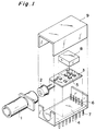
- the light-activated element, the lens system, and the sleeve must be assembled at high precision. For this reason, an optical module as shown in Fig. 1 is conventionally used.
- the optical module shown in Fig. 1 has a cylindrical holding body 1.
- the holding body 1 is formed of a metal such as stainless steel.
- a lens (not shown) is arranged in the holding body 1 at one end.
- the other end portion of the holding body 1 serves as a sleeve for receiving a ferrule (not shown) at the end portion of an optical fiber.
- a light-activated element 2 is fixed to the holding body 1 with an adhesive or the like.
- the light-activated element 2 is arranged such that the optical axes of the element 2, the ferrule connected to the holding body 1 and the lens are matched with each other.
- the holding body 1 having the light-activated element 2 fixed therein is supported, together with a circuit board 3, by a package main body 4 consisting of a ceramic or metal.
- the terminals of the light-activated element 2 are connected by soldering (not shown) to electronic components 5 such as bare chip ICs mounted on the circuit board 3.
- the package main body 4 has inner lead pins 6 mounted inside the body 4, and outer lead pins 7 mounted outside the body 4 and electrically connected to the inner lead pins 6.
- the inner lead pins 6 are electrically connected to terminals on the circuit board 3 by soldering.
- the wiring pattern and the electronic components 5 are sealed by a lid 8. Finally, a cover 9 is fixed to the package main body 4, thereby completing the optical module.
- the light-activated element 2 is held by the holding body 1 formed of a metal cylinder.
- the holding body 1 is an independent member which separates from the package main body 4 having the circuit board 3 mounted thereon and the cover 9. For this reason, there are many components of the module, resulting in higher productive cost and lower productive efficiency.
- an optical module in which a lead frame is used in place of a package main body and a cover.
- a circuit board and a light-activated element are mounted in the lead frame, and all these components are integrally molded with a plastic (Japanese Utility Model Laid-Open No. 2-126107).
- the light-activated element and the circuit board are independent members, as in the optical module shown in Fig. 1. Therefore, the same problem as in Fig. 1 is present.
- an object of the present invention to provide an optical module which can be easily and precisely assembled without using a cylindrical metal holding body.
- the constituent components of an optical module are integrally formed of a plastic.
- a light-activated element such as a light-emitting element or a light-receiving element, a lens, and a sleeve can be precisely arranged by plastic molding.
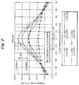
- the present inventor made an examination based on Fig. 2 and found that a precision required to couple light with a quartz optical fiber (graded-index type, core diameter: 62.5 ⁇ m) could be ⁇ 15 ⁇ m in a plane perpendicular to the optical axis and ⁇ 50 ⁇ m in a direction parallel to the optical axis. It was confirmed that, with this precision, the optical module could be realized with the dimensional precision of the plastic molding.
- Fig. 2 is a graph showing a relationship between a deviation in optical axis and an optical power wherein the quartz optical fiber and the light-activated element are separated from each other by a predetermined interval.
- This graph was obtained in the following manner. Two lenses were arranged between an end of the optical fiber and the light-activated element. The lens far from the end face of the optical fiber was defined as the first lens, and the lens closer to the end face of the optical fiber was defined as the second lens. The first lens was fixed, and the second lens was stationary with respect to the optical axis. In this state, the second lens was moved in the plane perpendicular to the optical axis, and variations in optical power of light coupled to the optical fiber were checked. Referring to Fig.
- L1 represents an interval between the first lens and the second lens
- L2 represents an interval between the second lens and the optical fiber.
- Fig. 2 shows variations in power of light in five arrangements obtained upon changing the position of the second lens along the optical axis.
- the present inventor found, from graphs indicated by symbol ⁇ and ⁇ , that a dimensional precision of ⁇ 15 ⁇ m was allowed in the plane perpendicular to the optical axis, and a dimensional precision of ⁇ 50 ⁇ m was allowed in the direction parallel to the optical axis.
- the present invention has been made on the basis of this examination.
- an optical module comprising a plastic package, constituted by a package main body and a cover for closing an open portion of the package main body, for receiving and holding a connector plug connected to an optical fiber, a sleeve formed integrally with the package main body by plastic molding to receive an end portion of the optical fiber when the connector plug is held in the package main body, a circuit board held in the open portion of the package main body, a light-activated element fixed at a predetermined position of the circuit board, three projections formed integrally with an inner surface of the package main body and brought into contact with a periphery of the circuit board to position the circuit board, spring means formed integrally with an inner surface of the package to press the periphery of the circuit board against the projections, and a condenser lens coaxially arranged in the sleeve.
- the sleeve and the package main body are integrally formed by plastic molding, the number of components is reduced, thereby simplifying the assembling steps.
- the circuit board is always supported by the projections at the predetermined reference points. Therefore, when the light-activated element is arranged at the predetermined position with respect to the reference points, the light-activated element, the sleeve, and the lens are coaxially arranged.
- a method of manufacturing an optical module having the above arrangement comprising the steps of preparing a board supporting table having three positioning pins standing on a surface in substantially the same layout as that of the three projections, resting the circuit board on the surface of the board supporting table, pressing the circuit board such that the periphery of the circuit board is brought into contact with all the pins, and using contact points of the pins as reference points to fix the light-activated element at a predetermined position with respect to the reference points.
- the positions where the circuit board is brought into contact with the projections in the package main body, i.e., the reference points can be easily specified by using the board supporting table having the positioning pins arranged in the same layout as that of the projections.
- the light-activated element can be arranged at a position where the light-activated element is aligned with the sleeve and the lens.
- FIGs. 3 to 7 are views showing an optical module according to an embodiment of the present invention.
- This optical module is of a transceiver type which integrates a transmission module and a reception module.
- reference numeral 10 designates an entire package formed by plastic molding.
- the package 10 comprises a package main body 12 and a cover 14 and serves as an optical connector receptacle for receiving connector plugs (not shown) provided at the end portions of transmission and reception optical fibers (not shown) to be connected.
- a circuit board 20 having ICs (not shown), a light-emitting element 16, a light-receiving element 18, and the like fixed thereon can be mounted-in the package 10.
- the package main body 12 is of a rectangular prism shape or parallelepiped box shape and has a pair of side plates 22 and 23 arranged parallel to each other, an upper plate 24 and a bottom plate 26.
- the upper and bottom plates 24 and 26 are arranged between the upper edges and between the lower edges of the side plates 22 and 23, respectively, to be parallel to each other.
- the side plates 22 and 23 and the upper plate 24 have almost the same length.
- the bottom plate 26 is shorter than the side plates 22 and 23 and the upper plate 24. One end of the bottom plate 26 is separated from the corresponding end portions of the side plates 22 and 23 and the upper plate 24 by a predetermined distance.
- a lateral plate 28 is arranged between the side plates 22 and 23 to perpendicularly extend from the end portion of the bottom plate 26 to the upper plate 24. Therefore, one end portion of the package main body 12 is closed by the lateral plate 28. The other end portion of the package main body 12 is open. The connector plug of the optical fiber is inserted into the open end portion.
- the open end portion side is conveniently referred to as a front side hereinafter.
- the side plates 22 and 23, the upper plate 24, the bottom plate 26, and the lateral plate 28 are integrally formed of an appropriate plastic material.
- a pair of sleeves 30 and 31 are arranged in the package main body 12 to receive the ferrules (not shown) at the end portions of the optical fibers and align each ferrule with the light-emitting element 16 or the light-receiving element 18 (to be described later).
- the sleeves 30 and 31 are parallelly arranged in the lateral direction to be separated from each other by a predetermined interval and extend forward (the open end portion side of the package main body 12) from the front surface of the lateral plate 28.
- the sleeves 30 and 31 consist of the same plastic material as that of the lateral plate 28 and the like and integrally formed on the lateral plate 28.
- Through holes 32 and 33 are formed in the lateral plate 28 at portions opposing the hollow portions of the sleeves 30 and 31. Together with the hollow portions of the sleeves 30 and 31, the through holes 32 and 33 form continuous holes which communicate the front inner portion to the rear inner portion of the package main body 12.
- the ferrules of the optical fibers are inserted into the corresponding sleeves 30 and 31 and supported by the inner surfaces of the sleeves 30 and 31 at desired positions.
- the sleeves 30 and 31 are not formed of a metal but a plastic, so the inner surfaces of the sleeves 30 and 31, which are in contact with the metal or ceramic ferrules, can be worn upon attachment and detachment of the connector plugs.
- the inner surfaces of the sleeves 30 and 31 must be precisely formed to determine the radial positions of the ferrules. For this reason, friction between the sleeves 30 and 31 and the ferrules is increased.
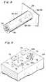
- a plurality of grooves 34 extending in the axial direction are formed in the inner surfaces of the sleeves 30 and 31, especially at portions in contact with the ferrule, and circumferentially spaced to each other, as shown in Fig. 8.
- a tapered portion 36 is preferably provided in the inner surface of the front end portion of the sleeve so that the ferrule can be smoothly inserted into the sleeve 30 or 31.
- Lenses 38 and 39 are respectively arranged inside the sleeves 30 and 31, more particularly, at appropriate locations of the portions of the sleeves on which the ferrules do not abut.
- the lenses 38 and 39 are positioned such that their optical axes match the longitudinal axes of the corresponding sleeves 30 and 31, respectively.
- the lens 38 mounted in the sleeve 30 opposing the light-emitting element 16 focuses light from the light-emitting element 16 on the central portion of the end face of the corresponding ferrule, i.e., the end face of the fiber core.
- the lens 39 mounted in the sleeve 31 focuses light emerging from the end face of the reception optical fiber on the light-receiving surface of the light-receiving element 18.
- the substantially rectangular circuit board 20 is arranged in a recessed portion (a portion defined by the inner surfaces of the side plates 22 and 23, the inner surface of the upper plate 24, and the rear surface of the lateral plate 28) 40 on the rear end portion side of the package main body 12.
- the circuit board 20 in this embodiment consists of a ceramic, an epoxy resin, or the like.
- a wiring pattern (not shown) is formed on the surface of the circuit board 20, and electronic components (not shown) such as ICs are mounted thereon.
- a circuit on the circuit board 20 is electrically connected to an external circuit by a plurality of lead pins 42 extending from the lower edge of the circuit board 20.
- the light-emitting element 16 such as a semiconductor laser or a light-emitting diode and the light-receiving element 18 are mounted on the surface of the circuit board 20 as light-activated elements.
- the light-emitting element 16 and the light-receiving element 18 are mounted such that the centers of the light-emitting and light-receiving surfaces almost match the central axes of the corresponding sleeves 30 and 31 when the circuit board 20 is arranged at a predetermined position in the package main body 12.
- a microball lens (not shown) at the center of the light-emitting surface of the light-emitting element 16 and fix it with a transparent adhesive or the like.
- a light-emitting element having a monolithic lens may be used.
- a transparent lid 44 of a plastic is fixed on the surface of the circuit board 20 by an adhesive.
- the wiring pattern, the electronic components, and the light-activated elements 16 and 18 on the surface of the circuit board are shielded from an atmosphere by the lid 44.
- the transparent lid 44 has a rectangular flat plate portion 46 which is slightly smaller than the circuit board 20, and a peripheral portion 48 formed integrally with the peripheral edges of the flat plate portion 46 and perpendicularly depends therefrom.
- the end face of the peripheral portion 48 of the transparent lid 44 is bonded to the surface of the circuit board 20. Therefore, a space is formed between the flat plate portion 46 of the transparent lid 44 and the surface of the circuit board 20, and the light-activated elements 16 and 18 and the like are arranged in this space.
- the circuit board 20 is arranged in the recessed portion 40 on the rear end portion side of the package main body 12.
- the circuit board 20 is accurately positioned by three positioning projections 50 to 52 formed on the inner surface of the package main body 12.
- one of the projections 50 to 52 is formed on the rear end portion side of the inner surface of the side plate 23, and the remaining projections are arranged in the lateral direction on the rear end portion side of the inner or lower surface of the upper plate 24 to be separated from each other by a predetermined interval.
- the projections 50 to 52 have a substantially semicircular section and extend along the longitudinal direction of the package main body 12.
- the circuit board 20 is arranged in a state wherein its periphery is pressed against the projections 50 to 52 and positioned.
- one long side of the rectangular circuit board 20, i.e., the upper edge is brought into contact with the projections 51 and 52 on the upper plate 24 of the package main body 12.
- one short side of the board 20, i.e., the right side edge in Fig. 3 is brought into contact with the projection 50 on the side plate 23.
- the circuit board 20 is supported at the three points, and its movements along two axial directions perpendicular to each other and in the rotational direction are limited.
- Springs 54 to 56 for pressing the circuit board 20 against the projections 50 to 52 are integrally formed on the rear end portion sides of the inner surfaces of the side plates 22 and 23 of the package main body 12. As shown in Fig.
- the spring 54 for pressing the circuit board 20 upward is formed, at a position adjacent to the lateral plate 28, on the inner surface of the side plate 23 having the projection 50.
- the spring 55 for pressing the circuit board 20 upward and the spring 56 for pressing the circuit board 20 toward the opposing side plate 23 are provided, at positions adjacent to the lateral plate 28, on the inner surface of the side plate 22.
- Various shapes of the springs 54 to 56 can be considered.
- each of the springs 54 to 56 is an arch-like projecting piece having one end integrally fixed to the side plate 22 or 23.
- the circuit board 20 When the circuit board 20 is arranged at a predetermined position to bring the surface of the flat plate portion 46 of the transparent lid 44 into contact with the rear surface of the lateral plate 28, the springs 54 to 56 are brought into contact with the outer surface of the peripheral portion 48 of the transparent lid 44, thereby pressing the transparent lid 44. At this time, the springs 54 to 56 do not directly press the circuit board 20. However, since the transparent lid 44 is fixed to the circuit board 20, the pressing forces of the springs 54 to 56 act on the circuit board 20 through the transparent lid 44, thereby pressing the circuit board 20 against the projections 50 to 52. The circuit board 20 pressed against the projections 50 to 52 by the springs 54 to 56 does not move in a plane defined by the surface of the circuit board 20.
- the package 10 of the optical module according to the present invention has the cover 14.
- the cover 14 closes the rear end portion of the package main body 12 to hold the circuit board 20.
- the cover 14 can be mounted at the rear end portion of the package main body 12 by dovetail joints. More specifically, dovetail-like projections 58 and 59 formed on the rear end surfaces of the side plates 22 and 23 of the package main body 12 are engaged with dovetail grooves 60 and 61 formed at the corresponding positions on the front surface of the cover 14, thereby jointing the cover 14 and the package main body 12.
- At least one (two in this embodiment) spring 62 is integrally formed on the front surface of the cover 14.
- the springs 62 press the lower surface of the circuit board 20 forward.
- the circuit board 20 is pressed forward, and the front surface of the flat plate portion 46 of the transparent lid 44 is brought into tight contact with the rear surface of the lateral plate 28, thereby arranging the circuit board 20 and the lateral plate 28 almost parallel to each other.
- the circuit board 20 is prevented from being separated from the springs 54 to 56 of the side plates 22 and 23, and at the same time, a deviation in optical axis is prevented.
- the lead pins 42 of the circuit board 20 externally extend from a gap between the cover 14 and the bottom plate 26 of the package main body 12 to enable connection to the external circuit.
- the circuit board 20 is accurately positioned with respect to the package main body 12. For this reason, the light-emitting element 16 and the light-receiving element 18 are coaxially arranged with the corresponding sleeves 30 and 31 and the internal lenses 38 and 39, respectively.
- the optical module of the present invention can be easily manufactured.
- the dimensional precision of an actually assembled optical module was checked, it was confirmed that the dimensional precision among the sleeves, the lenses, and the light-activated elements was ⁇ 15 ⁇ m or less in a plane perpendicular to the optical axis and ⁇ 50 ⁇ m or less in a direction parallel to the optical axis. This falls within a tolerance of the optical coupling efficiency when a quartz fiber (graded-index type, core diameter: 62.5 ⁇ m) is coupled to a light-activated element.
- circuit board 20 of a ceramic it is common that a large ceramic plate is divided along a predetermined line, thereby forming the circuit board 20. Generally, the periphery of the circuit board 20 obtained in this manner is not polished. Therefore, the size of the circuit board 20 varies for each product, and each edge does not form a perfect line.
- the light-emitting element 16 and the light-receiving element 18 may be mounted on the circuit board 20 using an apparatus as shown in Fig. 9.
- the light-activated element mounting apparatus in Fig. 9 includes a board supporting table 64 having a flat upper surface on which the circuit board 20 is to be mounted.
- Columnar pins 70 to 72 are mounted on and perpendicularly extend from the upper surface of the board supporting table 64 in the substantially same layout as that of the positioning projections 50 to 52 in the package main body 12. More specifically, the pins 70 to 72 are arranged such that points 50a, 51a, and 52a in Fig. 6 match points 70a, 71a, 72a in Fig. 9, respectively. These points is ones with which the circuit board 20 is brought into contact.
- the contact points of the pins 70 to 72 match the contact points of the positioning projections 50 to 52, respectively.
- the light-emitting element 16 and the light-receiving element 18 are arranged on the circuit board 20 at positions determined in advance with respect to the reference points. In this case, upon mounting the circuit board 20 in the package main body 12, the light-emitting element 16 and the light-receiving element 18 are arranged at predetermined positions in the package main body 12 regardless of the shape of the circuit board 20.
- the circuit board When the light-emitting element 16 and the light-receiving element 18 are to be actually mounted on the circuit board 20, first of all, the circuit board is rested on the board supporting table 64. Thereafter, forces as indicated by arrows 74 to 76 are caused to act on the circuit board 20, thereby holding the circuit board 20 on the board supporting table 64.
- the light-emitting element 16 and the light-receiving element 18 are fixed at predetermined positions using the contact points of the pins 70 to 72 as the reference points.
- a suitable manipulator such as a robot arm having a collet at the distal end thereof is preferably used.
- the mounting positions of the light-emitting element 16 and the light-receiving element 18 can be easily specified without using the above-described light-activated element mounting apparatus.
- bottomed holes (not shown) can be formed at the element mounting positions on the circuit board 20 in advance, and the light-activated elements 16 and 18 can be fitted in the holes, thereby accurately positioning the light-activated elements 16 and 18.
- a ground electrode or a lead electrode for inputting/outputting an electrical signal may be provided by metallization or the like on the inner wall and the bottom surface of the bottomed hole.
- Metallized portions may be formed to be used as the mounting positions of the light-activated elements 16 and 18 without forming the bottomed holes.
- the preferred embodiment of the present invention has been described above.
- the present invention is not limited to this embodiment, as a matter of course.
- the optical module of the above embodiment is a module used for both transmission and reception, and the light-emitting element 16 and the light-receiving element 18 are arranged on one circuit board 20.
- the present invention can also be applied to an optical module having only one function of transmission or reception.
- the springs 54 to 56 press the circuit board 20 through the transparent lid 44.
- the springs may directly press the circuit board 20.
- the springs 54 to 56 for pressing the circuit board 20 against the positioning projections 50 to 52 are formed on the package main body 12.
- these springs may be arranged on the remaining members constituting the package.
- a space portion 80 for arranging a circuit board 20' is formed at the central portion of a package main body 12' (Fig. 12).
- a cover 14' is mounted from the lower side of the circuit board 20' (Fig. 13). In this arrangement, as shown in Fig.
- a spring 56' for pressing the circuit board 20' against a positioning projection 50' on a side plate 23' of the package main body 12' is provided on the inner surface of a side plate 22', as in the above embodiment.
- springs 55' and 56' for pressing the circuit board 20' against positioning projections 51' and 52' on the lower surface of the upper plate 24 are provided to the cover 14'. In this case, when the cover is mounted, the circuit board 20' is simultaneously completely pressed against the projections 50' to 52', so the optical module can be more easily manufactured.
- the sleeves and the package main body are integrally formed of a plastic, and the light-activated elements are fixed on the circuit board in advance.
- the optical module can be assembled in the number of manufacturing steps smaller than that of the prior art. Therefore, the optical module can be provided at lower cost.
- the package is formed of a plastic, so mass production can be achieved.
- the circuit board is supported at the three points.
- This arrangement can cope with circuit boards having various shapes and sizes, so that a circuit board can always be supported at predetermined reference points. Therefore, when the light-activated elements are arranged at predetermined positions corresponding to the reference points, the light-activated elements, the sleeves, and the lenses can be coaxially arranged.
Landscapes
- Physics & Mathematics (AREA)
- General Physics & Mathematics (AREA)
- Optics & Photonics (AREA)
- Electromagnetism (AREA)
- Engineering & Computer Science (AREA)
- Computer Networks & Wireless Communication (AREA)
- Signal Processing (AREA)
- Optical Couplings Of Light Guides (AREA)
Priority Applications (1)
| Application Number | Priority Date | Filing Date | Title |
|---|---|---|---|
| EP01112865A EP1146371A3 (de) | 1993-09-30 | 1994-09-30 | Optisches Modul, Verfahren zu seiner Herstellung, und Hülse |
Applications Claiming Priority (3)
| Application Number | Priority Date | Filing Date | Title |
|---|---|---|---|
| JP245479/93 | 1993-09-30 | ||
| JP24547993 | 1993-09-30 | ||
| JP24547993 | 1993-09-30 |
Related Child Applications (1)
| Application Number | Title | Priority Date | Filing Date |
|---|---|---|---|
| EP01112865A Division EP1146371A3 (de) | 1993-09-30 | 1994-09-30 | Optisches Modul, Verfahren zu seiner Herstellung, und Hülse |
Publications (3)
| Publication Number | Publication Date |
|---|---|
| EP0646816A2 true EP0646816A2 (de) | 1995-04-05 |
| EP0646816A3 EP0646816A3 (de) | 1996-02-07 |
| EP0646816B1 EP0646816B1 (de) | 2002-01-23 |
Family
ID=17134280
Family Applications (2)
| Application Number | Title | Priority Date | Filing Date |
|---|---|---|---|
| EP01112865A Withdrawn EP1146371A3 (de) | 1993-09-30 | 1994-09-30 | Optisches Modul, Verfahren zu seiner Herstellung, und Hülse |
| EP94115441A Expired - Lifetime EP0646816B1 (de) | 1993-09-30 | 1994-09-30 | Optisches Modul und Verfahren zur Montage eines Fotowandlers über eine gedruckte Schaltung, die in diesem Modul anwendbar ist |
Family Applications Before (1)
| Application Number | Title | Priority Date | Filing Date |
|---|---|---|---|
| EP01112865A Withdrawn EP1146371A3 (de) | 1993-09-30 | 1994-09-30 | Optisches Modul, Verfahren zu seiner Herstellung, und Hülse |
Country Status (5)
| Country | Link |
|---|---|
| US (2) | US5475783A (de) |
| EP (2) | EP1146371A3 (de) |
| KR (1) | KR0139132B1 (de) |
| CA (1) | CA2133230C (de) |
| DE (1) | DE69429700T2 (de) |
Cited By (6)
| Publication number | Priority date | Publication date | Assignee | Title |
|---|---|---|---|---|
| GB2294125B (en) * | 1994-10-12 | 1998-09-02 | Methode Electronics Inc | Small footprint optoelectronic transceiver with laser |
| EP1063548A1 (de) | 1999-06-25 | 2000-12-27 | Lucent Technologies Inc. | Pastikverpacktes optoelektronisches Bauelement |
| US6729775B2 (en) | 1999-09-22 | 2004-05-04 | Infineon Technologies Ag | Electro-optical module with a housing |
| EP1248128A3 (de) * | 2001-04-03 | 2004-06-02 | Autonetworks Technologies, Ltd. | Optischer Stecker, Halterungsvorrichtung für optisches Element und Montageteil für einen optischen Stecker |
| EP1881352A1 (de) * | 2006-07-18 | 2008-01-23 | NEC Corporation | Optisches Sende-/Empfangsgerät |
| EP3855228A1 (de) * | 2020-01-21 | 2021-07-28 | Yazaki Corporation | Steckverbinder zur plattenmontage |
Families Citing this family (53)
| Publication number | Priority date | Publication date | Assignee | Title |
|---|---|---|---|---|
| USRE40150E1 (en) | 1994-04-25 | 2008-03-11 | Matsushita Electric Industrial Co., Ltd. | Fiber optic module |
| US5717533A (en) * | 1995-01-13 | 1998-02-10 | Methode Electronics Inc. | Removable optoelectronic module |
| US6220878B1 (en) | 1995-10-04 | 2001-04-24 | Methode Electronics, Inc. | Optoelectronic module with grounding means |
| US5598497A (en) * | 1995-07-14 | 1997-01-28 | Cogent Light Technologies, Inc. | Apparatus for mounting a light source within a system for coupling light into an optic fiber or fiber bundle |
| US6354747B1 (en) | 1996-08-26 | 2002-03-12 | Sumitomo Electric Industries, Ltd. | Optical module |
| DE69723630T2 (de) * | 1996-08-26 | 2004-04-15 | Sumitomo Electric Industries, Ltd. | Optoelektronisches Modul und Verfahren zu dessen Herstellung |
| JPH10123375A (ja) * | 1996-10-18 | 1998-05-15 | Ando Electric Co Ltd | 光モジュール用パッケージ |
| JP3514609B2 (ja) * | 1997-05-29 | 2004-03-31 | 新光電気工業株式会社 | 光半導体装置用リードフレームと光半導体装置 |
| JPH1154770A (ja) * | 1997-08-01 | 1999-02-26 | Kel Corp | 光コネクタ |
| DE19738168A1 (de) * | 1997-09-01 | 1999-03-11 | Bosch Gmbh Robert | Optoelektronisches Mikrosystem |
| SG71172A1 (en) | 1997-12-03 | 2000-03-21 | Sumitomo Electric Industries | Optical data link |
| US6239427B1 (en) | 1998-01-14 | 2001-05-29 | Sumitomo Electric Industries, Ltd. | Optical data link |
| US6203212B1 (en) * | 1998-08-24 | 2001-03-20 | Agilent Technologies, Inc. | Optical subassembly for use in fiber optic data transmission and reception |
| DE19845854C2 (de) * | 1998-10-05 | 2000-11-02 | Framatome Connectors Int | Lichtwellenleiter-Steckverbinder für eine mechanischlösbare Verbindung zwischen-mindestens einem LWL-Steckerpaar-mindestens einem LWL-Stecker und einer Leiterplatte |
| JP2000193849A (ja) | 1998-12-28 | 2000-07-14 | Yazaki Corp | 光コネクタ、スリ―ブ、及び、スリ―ブの製造方法 |
| US7013088B1 (en) | 1999-05-26 | 2006-03-14 | Jds Uniphase Corporation | Method and apparatus for parallel optical interconnection of fiber optic transmitters, receivers and transceivers |
| US6873800B1 (en) | 1999-05-26 | 2005-03-29 | Jds Uniphase Corporation | Hot pluggable optical transceiver in a small form pluggable package |
| US6901221B1 (en) | 1999-05-27 | 2005-05-31 | Jds Uniphase Corporation | Method and apparatus for improved optical elements for vertical PCB fiber optic modules |
| US6213651B1 (en) | 1999-05-26 | 2001-04-10 | E20 Communications, Inc. | Method and apparatus for vertical board construction of fiber optic transmitters, receivers and transceivers |
| US6632030B2 (en) | 1999-05-27 | 2003-10-14 | E20 Communications, Inc. | Light bending optical block for fiber optic modules |
| US7116912B2 (en) * | 1999-05-27 | 2006-10-03 | Jds Uniphase Corporation | Method and apparatus for pluggable fiber optic modules |
| US6952532B2 (en) | 1999-05-27 | 2005-10-04 | Jds Uniphase Corporation | Method and apparatus for multiboard fiber optic modules and fiber optic module arrays |
| KR100337702B1 (ko) * | 1999-05-31 | 2002-05-22 | 윤종용 | 초저가 트랜시버 모듈 |
| JP3760433B2 (ja) * | 1999-06-30 | 2006-03-29 | 矢崎総業株式会社 | レセプタクル |
| KR100349598B1 (ko) * | 2000-02-03 | 2002-08-23 | 삼성전자 주식회사 | 실리콘 광벤치를 이용한 스몰 폼 팩터 광송수신 집적 모듈 |
| JP3801464B2 (ja) * | 2000-07-03 | 2006-07-26 | 矢崎総業株式会社 | ハイブリッドコネクタ |
| JP3735011B2 (ja) * | 2000-07-03 | 2006-01-11 | 矢崎総業株式会社 | ハイブリッドコネクタの組み付け方法 |
| US6416238B1 (en) | 2000-08-07 | 2002-07-09 | Stratos Lightwave, Inc. | Modular high density multiple optical transmitter/receiver array |
| USD446770S1 (en) | 2000-09-29 | 2001-08-21 | Hon Hai Precision Ind. Co., Ltd. | Optielectrical connector |
| US6867377B2 (en) | 2000-12-26 | 2005-03-15 | Emcore Corporation | Apparatus and method of using flexible printed circuit board in optical transceiver device |
| US6799902B2 (en) | 2000-12-26 | 2004-10-05 | Emcore Corporation | Optoelectronic mounting structure |
| US7021836B2 (en) | 2000-12-26 | 2006-04-04 | Emcore Corporation | Attenuator and conditioner |
| US6905260B2 (en) | 2000-12-26 | 2005-06-14 | Emcore Corporation | Method and apparatus for coupling optical elements to optoelectronic devices for manufacturing optical transceiver modules |
| US6863444B2 (en) | 2000-12-26 | 2005-03-08 | Emcore Corporation | Housing and mounting structure |
| US6692161B2 (en) * | 2001-03-29 | 2004-02-17 | Intel Corporation | High frequency emitter and detector packaging scheme for 10GB/S transceiver |
| US20020154871A1 (en) * | 2001-04-19 | 2002-10-24 | Autonetworks Technologies, Ltd. | Optical connector, shield casing, optical connector device |
| TW468795U (en) * | 2001-05-30 | 2001-12-11 | Delta Electronics Inc | Optical transceiver |
| DE10130892C1 (de) * | 2001-06-27 | 2003-03-27 | Siemens Ag | Gehäuse für elektrische Baugruppen |
| GB0205529D0 (en) * | 2002-03-08 | 2002-04-24 | Agilent Technologies Inc | Module apparatus |
| JP2004126015A (ja) * | 2002-09-30 | 2004-04-22 | Matsushita Electric Works Ltd | 光電変換モジュール及びそれを用いる光レセプタクル |
| US6863453B2 (en) | 2003-01-28 | 2005-03-08 | Emcore Corporation | Method and apparatus for parallel optical transceiver module assembly |
| KR100613582B1 (ko) * | 2003-04-18 | 2006-08-17 | 가부시키가이샤 무라타 세이사쿠쇼 | 패키지 모듈 |
| US6969203B2 (en) * | 2003-04-29 | 2005-11-29 | Agilent Technologies, Inc. | Optical fiber receptacle, an optical fiber ferrule and an optical fiber receptacle and ferrule interconnection system |
| DE10332015A1 (de) * | 2003-07-14 | 2005-03-03 | Infineon Technologies Ag | Optoelektronisches Modul mit Senderchip und Verbindungsstück für das Modul zu einer optischen Faser und zu einer Schaltungsplatine, sowie Verfahren zur Herstellung derselben |
| US7685613B2 (en) * | 2005-01-18 | 2010-03-23 | Ronald Marc Permut | Combination storage extracting and biasing system |
| JP4523874B2 (ja) | 2005-06-01 | 2010-08-11 | ホシデン株式会社 | 光コネクタ |
| US8160451B2 (en) * | 2007-02-13 | 2012-04-17 | Finisar Corporation, Inc. | Optical network unit transceiver module with arrayed I/O video contacts |
| JP2009109992A (ja) * | 2007-10-09 | 2009-05-21 | Sumitomo Electric Ind Ltd | フェルール整列保持スリーブおよび光モジュール |
| WO2012099769A2 (en) * | 2011-01-20 | 2012-07-26 | Corning Incorporated | Receptacle ferrule assemblies with gradient index lenses and fiber optic connectors using same |
| CN107817564A (zh) * | 2012-10-30 | 2018-03-20 | 深圳迈辽技术转移中心有限公司 | 一种光电转换模组 |
| WO2015053625A1 (en) * | 2013-10-07 | 2015-04-16 | Ac Optomechanix | Receiving device and method for manufacturing such a receiving device |
| JP2019184745A (ja) | 2018-04-05 | 2019-10-24 | 矢崎総業株式会社 | 光コネクタ |
| DE102020123465B4 (de) * | 2020-09-09 | 2022-03-17 | HARTING Electronics GmbH | Optoelektronisches Modul, optoelektronischer Steckverbinder und optoelektronische Unterverteilung |
Family Cites Families (17)
| Publication number | Priority date | Publication date | Assignee | Title |
|---|---|---|---|---|
| US4134641A (en) * | 1977-05-17 | 1979-01-16 | International Telephone & Telegraph Corp. | Self centering connector design |
| DE3172553D1 (en) * | 1980-11-28 | 1985-11-07 | Toshiba Kk | Method for manufacturing a module for a fiber optic link |
| US4539476A (en) * | 1980-11-28 | 1985-09-03 | Tokyo Shibaura Denki Kabushiki Kaisha | Module for a fiber optic link |
| JPS5893017A (ja) * | 1981-11-30 | 1983-06-02 | Dai Ichi Seiko Co Ltd | 光コネクタ− |
| US4547039A (en) * | 1982-04-16 | 1985-10-15 | Amp Incorporated | Housing mountable on printed circuit board to interconnect fiber optic connectors |
| JPS60237410A (ja) * | 1984-05-11 | 1985-11-26 | Nec Corp | 光コネクタの接続スリ−ブ構造 |
| US5222170A (en) * | 1987-04-03 | 1993-06-22 | Bt&D Technologies Ltd. | Optical fiber device fabrication |
| US4840451A (en) * | 1987-12-08 | 1989-06-20 | Molex Incorporated | Shielded fiber optic connector assembly |
| JPH01169416A (ja) * | 1987-12-25 | 1989-07-04 | Hitachi Ltd | 光伝送モジュール |
| JP2640766B2 (ja) * | 1988-11-04 | 1997-08-13 | 大成建設株式会社 | レーザ変位計による2次元計測における相対角度の検出方法と装置 |
| US4979787A (en) * | 1990-01-12 | 1990-12-25 | Pco, Inc. | Optical-electronic interface module |
| US5117476A (en) * | 1990-01-19 | 1992-05-26 | Amp Incorporated | Optical transceiver package with insertable subassembly |
| DE69033400T2 (de) * | 1990-03-13 | 2000-05-11 | Sumitomo Electric Industries, Ltd. | Optisches Modul und Verfahren zu seiner Herstellung |
| US5071219A (en) * | 1990-11-09 | 1991-12-10 | General Motors Corporation | Fiber optic connection system and method |
| FR2694419B1 (fr) * | 1992-07-29 | 1994-09-02 | Cit Alcatel | Procédé de couplage d'une fibre optique à un composant sur un substrat commun. |
| DE69318900T2 (de) * | 1992-08-11 | 1998-10-01 | Sumitomo Electric Industries | Optisches Modul mit verbesserter Erdung eines optischen Elements |
| US5379362A (en) * | 1993-02-24 | 1995-01-03 | Sumitomo Wiring Systems, Ltd. | Optical fiber connector |
-
1994
- 1994-09-29 US US08/314,652 patent/US5475783A/en not_active Expired - Lifetime
- 1994-09-29 KR KR1019940024690A patent/KR0139132B1/ko not_active Expired - Fee Related
- 1994-09-29 CA CA002133230A patent/CA2133230C/en not_active Expired - Fee Related
- 1994-09-30 EP EP01112865A patent/EP1146371A3/de not_active Withdrawn
- 1994-09-30 DE DE69429700T patent/DE69429700T2/de not_active Expired - Fee Related
- 1994-09-30 EP EP94115441A patent/EP0646816B1/de not_active Expired - Lifetime
-
1995
- 1995-09-20 US US08/531,006 patent/US5633971A/en not_active Expired - Lifetime
Cited By (10)
| Publication number | Priority date | Publication date | Assignee | Title |
|---|---|---|---|---|
| GB2294125B (en) * | 1994-10-12 | 1998-09-02 | Methode Electronics Inc | Small footprint optoelectronic transceiver with laser |
| EP1063548A1 (de) | 1999-06-25 | 2000-12-27 | Lucent Technologies Inc. | Pastikverpacktes optoelektronisches Bauelement |
| US6729775B2 (en) | 1999-09-22 | 2004-05-04 | Infineon Technologies Ag | Electro-optical module with a housing |
| EP1248128A3 (de) * | 2001-04-03 | 2004-06-02 | Autonetworks Technologies, Ltd. | Optischer Stecker, Halterungsvorrichtung für optisches Element und Montageteil für einen optischen Stecker |
| US6860643B2 (en) | 2001-04-03 | 2005-03-01 | Autonetworks Technologies, Limited | Optical connector with a surface mounted shield |
| EP1524538A1 (de) * | 2001-04-03 | 2005-04-20 | Autonetworks Technologies, Ltd. | Optischer Stecker, Halterungsvorrichtung für optisches Element und Montageteil für einen optischen Stecker |
| US6939054B2 (en) | 2001-04-03 | 2005-09-06 | Autonetworks Technologies, Ltd. | Holding structures for optical elements of an optical connector |
| EP1881352A1 (de) * | 2006-07-18 | 2008-01-23 | NEC Corporation | Optisches Sende-/Empfangsgerät |
| CN101726809B (zh) * | 2006-07-18 | 2012-05-30 | 日本电气株式会社 | 光学收发器 |
| EP3855228A1 (de) * | 2020-01-21 | 2021-07-28 | Yazaki Corporation | Steckverbinder zur plattenmontage |
Also Published As
| Publication number | Publication date |
|---|---|
| EP1146371A3 (de) | 2002-01-09 |
| CA2133230C (en) | 2004-06-29 |
| EP0646816A3 (de) | 1996-02-07 |
| KR0139132B1 (ko) | 1998-07-01 |
| KR950010414A (ko) | 1995-04-28 |
| DE69429700T2 (de) | 2002-09-12 |
| DE69429700D1 (de) | 2002-03-14 |
| CA2133230A1 (en) | 1995-03-31 |
| US5633971A (en) | 1997-05-27 |
| US5475783A (en) | 1995-12-12 |
| EP0646816B1 (de) | 2002-01-23 |
| EP1146371A2 (de) | 2001-10-17 |
Similar Documents
| Publication | Publication Date | Title |
|---|---|---|
| US5475783A (en) | Optical module, method of manufacturing the same, and sleeve | |
| US5666449A (en) | Optical waveguide device | |
| US8079125B2 (en) | Manufacturing method of multi-channel optical module | |
| US6056448A (en) | Vertical cavity surface emitting laser array packaging | |
| EP0446410B1 (de) | Optisches Modul und Verfahren zu seiner Herstellung | |
| US6913400B2 (en) | Optoelectric module for multi-fiber arrays | |
| TW392078B (en) | Stubless optoelectronic device receptacle | |
| CA2036727C (en) | Optical module including receptacle, and method of producing the same | |
| US5963693A (en) | Optical data link and method of manufacturing the same | |
| US7050678B1 (en) | Optical module, optical element attachment method, and receptacle-fitted optical module | |
| KR20170012339A (ko) | 광전 디바이스로의 광파이버 서브조립체의 비전 기반 피동 정렬 | |
| US7625133B2 (en) | Method of assembling optoelectronic devices and an optoelectronic device assembled according to this method | |
| EP0921426A1 (de) | Optische datenverbindung | |
| JPH07177086A (ja) | 光モジュール、その製造方法及びスリーブ | |
| WO2001027675A1 (en) | Interface between opto-electronic devices and fibers | |
| CA2359002C (en) | Optoelectric module for multi-fiber arrays | |
| JP4543561B2 (ja) | 光モジュールの製造方法、及び光モジュール | |
| JP2973542B2 (ja) | 光モジュール及びその製造装置及びその製造方法 | |
| JP2003185892A (ja) | 光接続用スリーブ、光モジュール、及び光通信モジュール | |
| EP3872546B1 (de) | Optischer verbinder und optische verbindervorrichtung | |
| JP4056294B2 (ja) | 光ファイバ端末固定方法及び光学系サブユニット | |
| JP2973532B2 (ja) | 多心式光モジュール | |
| JPH02278212A (ja) | 多心式光モジュール及びその製造方法 | |
| JPH09145961A (ja) | 半導体光結合装置 | |
| JPH11326706A (ja) | レセプタクル形光モジュール |
Legal Events
| Date | Code | Title | Description |
|---|---|---|---|
| PUAI | Public reference made under article 153(3) epc to a published international application that has entered the european phase |
Free format text: ORIGINAL CODE: 0009012 |
|
| AK | Designated contracting states |
Kind code of ref document: A2 Designated state(s): DE FR GB SE |
|
| PUAL | Search report despatched |
Free format text: ORIGINAL CODE: 0009013 |
|
| AK | Designated contracting states |
Kind code of ref document: A3 Designated state(s): DE FR GB SE |
|
| 17P | Request for examination filed |
Effective date: 19960327 |
|
| 17Q | First examination report despatched |
Effective date: 19990517 |
|
| RTI1 | Title (correction) |
Free format text: OPTICAL MODULE, AND METHOD OF MOUNTING A PHOTOTRANSDUCER ELEMENT ON A CIRCUIT BOARD TO BE USED IN SAID MODULE |
|
| GRAG | Despatch of communication of intention to grant |
Free format text: ORIGINAL CODE: EPIDOS AGRA |
|
| GRAG | Despatch of communication of intention to grant |
Free format text: ORIGINAL CODE: EPIDOS AGRA |
|
| GRAH | Despatch of communication of intention to grant a patent |
Free format text: ORIGINAL CODE: EPIDOS IGRA |
|
| GRAH | Despatch of communication of intention to grant a patent |
Free format text: ORIGINAL CODE: EPIDOS IGRA |
|
| GRAA | (expected) grant |
Free format text: ORIGINAL CODE: 0009210 |
|
| REG | Reference to a national code |
Ref country code: GB Ref legal event code: IF02 |
|
| AK | Designated contracting states |
Kind code of ref document: B1 Designated state(s): DE FR GB SE |
|
| REF | Corresponds to: |
Ref document number: 69429700 Country of ref document: DE Date of ref document: 20020314 |
|
| ET | Fr: translation filed | ||
| PLBE | No opposition filed within time limit |
Free format text: ORIGINAL CODE: 0009261 |
|
| STAA | Information on the status of an ep patent application or granted ep patent |
Free format text: STATUS: NO OPPOSITION FILED WITHIN TIME LIMIT |
|
| 26N | No opposition filed | ||
| PGFP | Annual fee paid to national office [announced via postgrant information from national office to epo] |
Ref country code: SE Payment date: 20040906 Year of fee payment: 11 |
|
| PGFP | Annual fee paid to national office [announced via postgrant information from national office to epo] |
Ref country code: FR Payment date: 20040908 Year of fee payment: 11 |
|
| PGFP | Annual fee paid to national office [announced via postgrant information from national office to epo] |
Ref country code: DE Payment date: 20040923 Year of fee payment: 11 |
|
| PGFP | Annual fee paid to national office [announced via postgrant information from national office to epo] |
Ref country code: GB Payment date: 20040929 Year of fee payment: 11 |
|
| PG25 | Lapsed in a contracting state [announced via postgrant information from national office to epo] |
Ref country code: GB Free format text: LAPSE BECAUSE OF NON-PAYMENT OF DUE FEES Effective date: 20050930 |
|
| PG25 | Lapsed in a contracting state [announced via postgrant information from national office to epo] |
Ref country code: SE Free format text: LAPSE BECAUSE OF NON-PAYMENT OF DUE FEES Effective date: 20051001 |
|
| PG25 | Lapsed in a contracting state [announced via postgrant information from national office to epo] |
Ref country code: DE Free format text: LAPSE BECAUSE OF NON-PAYMENT OF DUE FEES Effective date: 20060401 |
|
| GBPC | Gb: european patent ceased through non-payment of renewal fee |
Effective date: 20050930 |
|
| PG25 | Lapsed in a contracting state [announced via postgrant information from national office to epo] |
Ref country code: FR Free format text: LAPSE BECAUSE OF NON-PAYMENT OF DUE FEES Effective date: 20060531 |
|
| EUG | Se: european patent has lapsed | ||
| REG | Reference to a national code |
Ref country code: FR Ref legal event code: ST Effective date: 20060531 |