EP0606162A2 - Bildanzeigesystem mit Mosaikmustern aus Pixeln - Google Patents
Bildanzeigesystem mit Mosaikmustern aus Pixeln Download PDFInfo
- Publication number
- EP0606162A2 EP0606162A2 EP94300080A EP94300080A EP0606162A2 EP 0606162 A2 EP0606162 A2 EP 0606162A2 EP 94300080 A EP94300080 A EP 94300080A EP 94300080 A EP94300080 A EP 94300080A EP 0606162 A2 EP0606162 A2 EP 0606162A2
- Authority
- EP
- European Patent Office
- Prior art keywords
- optical path
- image
- image display
- pixels
- display system
- Prior art date
- Legal status (The legal status is an assumption and is not a legal conclusion. Google has not performed a legal analysis and makes no representation as to the accuracy of the status listed.)
- Granted
Links
Images


Classifications
-
- C—CHEMISTRY; METALLURGY
- C03—GLASS; MINERAL OR SLAG WOOL
- C03B—MANUFACTURE, SHAPING, OR SUPPLEMENTARY PROCESSES
- C03B37/00—Manufacture or treatment of flakes, fibres, or filaments from softened glass, minerals, or slags
- C03B37/01—Manufacture of glass fibres or filaments
- C03B37/012—Manufacture of preforms for drawing fibres or filaments
- C03B37/014—Manufacture of preforms for drawing fibres or filaments made entirely or partially by chemical means, e.g. vapour phase deposition of bulk porous glass either by outside vapour deposition [OVD], or by outside vapour phase oxidation [OVPO] or by vapour axial deposition [VAD]
- C03B37/01486—Means for supporting, rotating or translating the preforms being formed, e.g. lathes
-
- G—PHYSICS
- G02—OPTICS
- G02F—OPTICAL DEVICES OR ARRANGEMENTS FOR THE CONTROL OF LIGHT BY MODIFICATION OF THE OPTICAL PROPERTIES OF THE MEDIA OF THE ELEMENTS INVOLVED THEREIN; NON-LINEAR OPTICS; FREQUENCY-CHANGING OF LIGHT; OPTICAL LOGIC ELEMENTS; OPTICAL ANALOGUE/DIGITAL CONVERTERS
- G02F1/00—Devices or arrangements for the control of the intensity, colour, phase, polarisation or direction of light arriving from an independent light source, e.g. switching, gating or modulating; Non-linear optics
- G02F1/01—Devices or arrangements for the control of the intensity, colour, phase, polarisation or direction of light arriving from an independent light source, e.g. switching, gating or modulating; Non-linear optics for the control of the intensity, phase, polarisation or colour
- G02F1/13—Devices or arrangements for the control of the intensity, colour, phase, polarisation or direction of light arriving from an independent light source, e.g. switching, gating or modulating; Non-linear optics for the control of the intensity, phase, polarisation or colour based on liquid crystals, e.g. single liquid crystal display cells
- G02F1/133—Constructional arrangements; Operation of liquid crystal cells; Circuit arrangements
- G02F1/1333—Constructional arrangements; Manufacturing methods
- G02F1/1335—Structural association of cells with optical devices, e.g. polarisers or reflectors
- G02F1/133504—Diffusing, scattering, diffracting elements
-
- G—PHYSICS
- G09—EDUCATION; CRYPTOGRAPHY; DISPLAY; ADVERTISING; SEALS
- G09G—ARRANGEMENTS OR CIRCUITS FOR CONTROL OF INDICATING DEVICES USING STATIC MEANS TO PRESENT VARIABLE INFORMATION
- G09G3/00—Control arrangements or circuits, of interest only in connection with visual indicators other than cathode-ray tubes
- G09G3/001—Control arrangements or circuits, of interest only in connection with visual indicators other than cathode-ray tubes using specific devices not provided for in groups G09G3/02 - G09G3/36, e.g. using an intermediate record carrier such as a film slide; Projection systems; Display of non-alphanumerical information, solely or in combination with alphanumerical information, e.g. digital display on projected diapositive as background
-
- G—PHYSICS
- G09—EDUCATION; CRYPTOGRAPHY; DISPLAY; ADVERTISING; SEALS
- G09G—ARRANGEMENTS OR CIRCUITS FOR CONTROL OF INDICATING DEVICES USING STATIC MEANS TO PRESENT VARIABLE INFORMATION
- G09G3/00—Control arrangements or circuits, of interest only in connection with visual indicators other than cathode-ray tubes
- G09G3/007—Use of pixel shift techniques, e.g. by mechanical shift of the physical pixels or by optical shift of the perceived pixels
-
- G—PHYSICS
- G09—EDUCATION; CRYPTOGRAPHY; DISPLAY; ADVERTISING; SEALS
- G09G—ARRANGEMENTS OR CIRCUITS FOR CONTROL OF INDICATING DEVICES USING STATIC MEANS TO PRESENT VARIABLE INFORMATION
- G09G3/00—Control arrangements or circuits, of interest only in connection with visual indicators other than cathode-ray tubes
- G09G3/20—Control arrangements or circuits, of interest only in connection with visual indicators other than cathode-ray tubes for presentation of an assembly of a number of characters, e.g. a page, by composing the assembly by combination of individual elements arranged in a matrix no fixed position being assigned to or needed to be assigned to the individual characters or partial characters
- G09G3/34—Control arrangements or circuits, of interest only in connection with visual indicators other than cathode-ray tubes for presentation of an assembly of a number of characters, e.g. a page, by composing the assembly by combination of individual elements arranged in a matrix no fixed position being assigned to or needed to be assigned to the individual characters or partial characters by control of light from an independent source
- G09G3/36—Control arrangements or circuits, of interest only in connection with visual indicators other than cathode-ray tubes for presentation of an assembly of a number of characters, e.g. a page, by composing the assembly by combination of individual elements arranged in a matrix no fixed position being assigned to or needed to be assigned to the individual characters or partial characters by control of light from an independent source using liquid crystals
-
- G—PHYSICS
- G09—EDUCATION; CRYPTOGRAPHY; DISPLAY; ADVERTISING; SEALS
- G09G—ARRANGEMENTS OR CIRCUITS FOR CONTROL OF INDICATING DEVICES USING STATIC MEANS TO PRESENT VARIABLE INFORMATION
- G09G5/00—Control arrangements or circuits for visual indicators common to cathode-ray tube indicators and other visual indicators
-
- H—ELECTRICITY
- H04—ELECTRIC COMMUNICATION TECHNIQUE
- H04N—PICTORIAL COMMUNICATION, e.g. TELEVISION
- H04N23/00—Cameras or camera modules comprising electronic image sensors; Control thereof
- H04N23/60—Control of cameras or camera modules
- H04N23/68—Control of cameras or camera modules for stable pick-up of the scene, e.g. compensating for camera body vibrations
- H04N23/682—Vibration or motion blur correction
- H04N23/685—Vibration or motion blur correction performed by mechanical compensation
- H04N23/686—Vibration or motion blur correction performed by mechanical compensation with a variable apex prism
-
- H—ELECTRICITY
- H04—ELECTRIC COMMUNICATION TECHNIQUE
- H04N—PICTORIAL COMMUNICATION, e.g. TELEVISION
- H04N23/00—Cameras or camera modules comprising electronic image sensors; Control thereof
- H04N23/60—Control of cameras or camera modules
- H04N23/68—Control of cameras or camera modules for stable pick-up of the scene, e.g. compensating for camera body vibrations
- H04N23/682—Vibration or motion blur correction
- H04N23/685—Vibration or motion blur correction performed by mechanical compensation
- H04N23/687—Vibration or motion blur correction performed by mechanical compensation by shifting the lens or sensor position
-
- H—ELECTRICITY
- H04—ELECTRIC COMMUNICATION TECHNIQUE
- H04N—PICTORIAL COMMUNICATION, e.g. TELEVISION
- H04N3/00—Scanning details of television systems; Combination thereof with generation of supply voltages
- H04N3/10—Scanning details of television systems; Combination thereof with generation of supply voltages by means not exclusively optical-mechanical
- H04N3/12—Scanning details of television systems; Combination thereof with generation of supply voltages by means not exclusively optical-mechanical by switched stationary formation of lamps, photocells or light relays
- H04N3/127—Scanning details of television systems; Combination thereof with generation of supply voltages by means not exclusively optical-mechanical by switched stationary formation of lamps, photocells or light relays using liquid crystals
-
- H—ELECTRICITY
- H04—ELECTRIC COMMUNICATION TECHNIQUE
- H04N—PICTORIAL COMMUNICATION, e.g. TELEVISION
- H04N5/00—Details of television systems
- H04N5/74—Projection arrangements for image reproduction, e.g. using eidophor
- H04N5/7416—Projection arrangements for image reproduction, e.g. using eidophor involving the use of a spatial light modulator, e.g. a light valve, controlled by a video signal
- H04N5/7441—Projection arrangements for image reproduction, e.g. using eidophor involving the use of a spatial light modulator, e.g. a light valve, controlled by a video signal the modulator being an array of liquid crystal cells
-
- H—ELECTRICITY
- H04—ELECTRIC COMMUNICATION TECHNIQUE
- H04N—PICTORIAL COMMUNICATION, e.g. TELEVISION
- H04N5/00—Details of television systems
- H04N5/76—Television signal recording
- H04N5/765—Interface circuits between an apparatus for recording and another apparatus
- H04N5/77—Interface circuits between an apparatus for recording and another apparatus between a recording apparatus and a television camera
-
- H—ELECTRICITY
- H04—ELECTRIC COMMUNICATION TECHNIQUE
- H04N—PICTORIAL COMMUNICATION, e.g. TELEVISION
- H04N5/00—Details of television systems
- H04N5/76—Television signal recording
- H04N5/91—Television signal processing therefor
- H04N5/92—Transformation of the television signal for recording, e.g. modulation, frequency changing; Inverse transformation for playback
- H04N5/9201—Transformation of the television signal for recording, e.g. modulation, frequency changing; Inverse transformation for playback involving the multiplexing of an additional signal and the video signal
- H04N5/9206—Transformation of the television signal for recording, e.g. modulation, frequency changing; Inverse transformation for playback involving the multiplexing of an additional signal and the video signal the additional signal being a character code signal
-
- H—ELECTRICITY
- H04—ELECTRIC COMMUNICATION TECHNIQUE
- H04N—PICTORIAL COMMUNICATION, e.g. TELEVISION
- H04N9/00—Details of colour television systems
- H04N9/12—Picture reproducers
-
- H—ELECTRICITY
- H04—ELECTRIC COMMUNICATION TECHNIQUE
- H04N—PICTORIAL COMMUNICATION, e.g. TELEVISION
- H04N9/00—Details of colour television systems
- H04N9/12—Picture reproducers
- H04N9/30—Picture reproducers using solid-state colour display devices
-
- G—PHYSICS
- G02—OPTICS
- G02F—OPTICAL DEVICES OR ARRANGEMENTS FOR THE CONTROL OF LIGHT BY MODIFICATION OF THE OPTICAL PROPERTIES OF THE MEDIA OF THE ELEMENTS INVOLVED THEREIN; NON-LINEAR OPTICS; FREQUENCY-CHANGING OF LIGHT; OPTICAL LOGIC ELEMENTS; OPTICAL ANALOGUE/DIGITAL CONVERTERS
- G02F1/00—Devices or arrangements for the control of the intensity, colour, phase, polarisation or direction of light arriving from an independent light source, e.g. switching, gating or modulating; Non-linear optics
- G02F1/01—Devices or arrangements for the control of the intensity, colour, phase, polarisation or direction of light arriving from an independent light source, e.g. switching, gating or modulating; Non-linear optics for the control of the intensity, phase, polarisation or colour
- G02F1/13—Devices or arrangements for the control of the intensity, colour, phase, polarisation or direction of light arriving from an independent light source, e.g. switching, gating or modulating; Non-linear optics for the control of the intensity, phase, polarisation or colour based on liquid crystals, e.g. single liquid crystal display cells
- G02F1/133—Constructional arrangements; Operation of liquid crystal cells; Circuit arrangements
- G02F1/1333—Constructional arrangements; Manufacturing methods
- G02F1/1335—Structural association of cells with optical devices, e.g. polarisers or reflectors
- G02F1/13363—Birefringent elements, e.g. for optical compensation
-
- G—PHYSICS
- G02—OPTICS
- G02F—OPTICAL DEVICES OR ARRANGEMENTS FOR THE CONTROL OF LIGHT BY MODIFICATION OF THE OPTICAL PROPERTIES OF THE MEDIA OF THE ELEMENTS INVOLVED THEREIN; NON-LINEAR OPTICS; FREQUENCY-CHANGING OF LIGHT; OPTICAL LOGIC ELEMENTS; OPTICAL ANALOGUE/DIGITAL CONVERTERS
- G02F1/00—Devices or arrangements for the control of the intensity, colour, phase, polarisation or direction of light arriving from an independent light source, e.g. switching, gating or modulating; Non-linear optics
- G02F1/01—Devices or arrangements for the control of the intensity, colour, phase, polarisation or direction of light arriving from an independent light source, e.g. switching, gating or modulating; Non-linear optics for the control of the intensity, phase, polarisation or colour
- G02F1/13—Devices or arrangements for the control of the intensity, colour, phase, polarisation or direction of light arriving from an independent light source, e.g. switching, gating or modulating; Non-linear optics for the control of the intensity, phase, polarisation or colour based on liquid crystals, e.g. single liquid crystal display cells
- G02F1/133—Constructional arrangements; Operation of liquid crystal cells; Circuit arrangements
- G02F1/1333—Constructional arrangements; Manufacturing methods
- G02F1/1347—Arrangement of liquid crystal layers or cells in which the final condition of one light beam is achieved by the addition of the effects of two or more layers or cells
- G02F1/13471—Arrangement of liquid crystal layers or cells in which the final condition of one light beam is achieved by the addition of the effects of two or more layers or cells in which all the liquid crystal cells or layers remain transparent, e.g. FLC, ECB, DAP, HAN, TN, STN, SBE-LC cells
Definitions
- the present invention relates to an image display system such as a liquid crystal display (LCD) system for displaying image information with a three-dimensional matrix of pixels arranged in horizontal rows and vertical columns, and more particularly to a method of and an apparatus for increasing the apparent number of pixels to improve the resolution of displayed images in such an image display system, and an imaging apparatus which is capable of increasing the apparent number of pixels to improve the resolution of images produced thereby.
- LCD liquid crystal display
- an image display system such as an LCD system for displaying image information with a three-dimensional matrix of pixels arranged in horizontal rows and vertical columns.
- a horizontally repeated pattern of vertical stripe filters of three primaries i.e., red, green, and blue
- each vertical stripe filter being aligned with one vertical column of pixels.
- one vertical stripe filter of a certain primary exists in every three vertical columns of pixels, the color images displayed on the image display system suffer a poor horizontal resolution.
- the conventional image display system displays an image according to an interlaced scanning process in which an image pattern of an odd-numbered field and an image pattern of an even-numbered field are successively displayed on the same pixels, so that the image can be displayed with a small number of pixels.
- the interlaced scanning process effected on the conventional image display system has a problem in that it fails to achieve a sufficient level of resolution.
- Displaying an image on the image display system according to a noninterlaced scanning process requires that the number of pixels in the vertical direction be twice that which is necessary by the interlaced scanning process. However, if the number of pixels is increased for higher resolution in the image display system that is composed of a cluster of pixels, then the vignetting factor of the image display system is lowered, and dot defects are produced resulting in a lower yield and a higher cost.
- the noninterlaced scanning process also requires a memory for storing one horizontal line or field of image information, and makes the arrangement for driving the image display system complex.
- Another object of the present invention is to provide an imaging apparatus which is capable of optically increasing the apparent number of pixels to improve the resolution of images produced thereby.
- a method of increasing the resolution of an image on an image display system having a matrix of pixels arranged in horizontal rows and vertical columns and selectively energizable to display an image composed of a plurality of pixel patterns in alternate fields comprising the steps of positioning an optical path changer between the image display system and a viewer or screen for shifting an optical path therebetween to optically shift a pixel pattern, operating the optical path changer to shift the optical path, and displaying the pixel pattern to be optically shifted on the image display system in every field in synchronism with the shifting of the optical path by the optical path changer.
- the optical path can also be changed or shifted horizontally.
- the optical path is horizontally shifted in every field and pixel patterns to be shifted horizontally are displayed in timed relation to the horizontal changing of the optical path, the number of pixels can also be apparently increased in the horizontal direction.
- an image display system comprising an image display device having a matrix of pixels arranged in horizontal rows and vertical columns and selectively energizable to display an image composed of a plurality of pixel patterns in alternate fields, an optical path changer disposed between the image display device and a viewer or screen for shifting an optical path therebetween to optically shift pixel patterns, and shifting means for shifting pixel patterns displayed on the image display device in timed relation to the change of the optical path by the optical path changer.
- a method of increasing the resolution of an image on an image display system having a pair of projectors each having a liquid-crystal display device having a matrix of pixels for displaying an image in an interlaced scanned process and means for projecting the displayed image onto a screen, comprising the steps of controlling one of the projectors to display only odd-numbered fields of image information on the screen, controlling the other of the projectors to display only even-numbered fields of image information on the screen, and shifting respective images projected onto the screen by the projectors vertically from each other by 1/2 of the pitch of the pixels.
- a method of increasing the resolution of an image on an image display system having a matrix of pixels arranged in horizontal rows and vertical columns and selectively energizable to display an image composed of a plurality of pixel patterns in alternate fields, the pixels being capable of continuously displaying the image until next image information is supplied to the pixels, comprising the steps of positioning an optical path changer between the image display system and a viewer or screen for shifting an optical path therebetween depending on the pixel pattern to be displayed in synchronism with vertical scanning on the image display system, operating the optical path changer to shift the optical path, and displaying the pixel pattern to be optically shifted on the image display system in every field in synchronism with the shifting of the optical path by the optical path changer.
- an imaging apparatus comprising an imaging unit having a matrix of pixels for producing an image signal from all the pixels in every field in a noninterlaced scanning process, an optical path changer disposed between the imaging unit and a subject to be imaged by the imaging unit to shift an optical path therebetween, and actuator means for actuating the optical path changer to shift the optical path in a predetermined direction in every field or frame in response to a shock applied to the imaging unit, whereby the image signal generated by the imaging unit is free from suffering the shock.
- a recording apparatus comprising an imaging unit, an optical path changer disposed between the imaging unit and a subject to be imaged by the imaging unit to shift an optical path therebetween, means for controlling the optical path changer to shift the optical path in every field or frame, and means for recording, on a recording medium, a plurality of field images of the subject whose optical paths are shifted by the optical path changer and have different spatially sampled positions, together with information representative of a quantity by and a direction in which each of the field images is shifted.
- a reproducing apparatus for playing back the recording medium which has been recorded by the above recording apparatus, comprising means for extracting the field images and the information representative of a quantity by and a direction in which each of the field images is shifted, from a reproduced signal supplied from the recording medium, and means for shifting the extracted field images vertically and horizontally based on the extracted information and combining the shifted field images into a still image of high resolution.
- FIGS. 1A through 1C and 3A through 3C show staggered patterns of three-primary pixels, which are actually composed of pixels and filters of three primaries of red (R), green (G), and blue (B) disposed in front of the pixels, for use in a color image display system.
- the positions of displayed pixels are optically shifted vertically for allowing the viewer of an image produced by the pixels to see the image as if the pixels were present on the optically shifted positions, and the image is displayed on the color image display system.
- FIG. 1A shows a color pixel pattern which comprises a staggered matrix of three-primary pixels that is not optically shifted in any direction.
- the pixels are spaced horizontally by a pitch PH and vertically by a pitch Pv.
- FIG. 1B shows a color pixel pattern which also comprises a staggered matrix of three-primary pixels that is optically shifted vertically downwardly from the color pixel pattern shown in FIG. 1A by 1/2 of the vertical pitch Pv as seen by the viewer.
- the color pixel pattern shown in FIG. 1B is optically shifted by an optical path changer (described - later on).
- the color pixel pattern shown in FIG. 1A is supplied with image information VA composed of pixel information at the pixel positions shown in FIG. 1A.
- the color pixel pattern shown in FIG. 1B is supplied with image information VB composed of pixel information at the pixel positions shown in FIG. 1B.
- the image information VA, VB contains respective pixel information at the pixel positions that are vertically shifted Pv/2 from each other with respect to an image that is to be displayed.
- the optical path changer is controlled such that the color pixel patterns shown in FIGS. 1A and 1B which are visually vertically shifted Pv/2 from each other will visually be observed as alternating fields by the viewer.
- the image information VA, VB is switched each field and supplied to the color image display system, i.e., the image information VA is supplied in one field and the image information VB is supplied in the next field to the color image display system, so that the color pixel patterns shown in FIGS. 1A and 1B will be displayed alternately in respective fields.
- the color image display system apparently displays a color image with a resolution which is substantially the same as a color image display system having twice as many pixels as the illustrated pixels.
- the positions of displayed pixels are optically shifted both vertically and horizontally.
- the positions of displayed pixels are optically shifted Pv/2 vertically, and Pc/2 horizontally where Pc is the pitch of pixels of the same colors in the horizontal direction.
- FIG. 2A shows a color pixel pattern PTA which comprises a staggered matrix of three-primary pixels that is not optically shifted in any direction.
- FIG. 2B shows a color pixel pattern PTC which also comprises a staggered matrix of three-primary pixels that is optically shifted Pv/2 vertically downwardly and Pc/2 horizontally to the right from the color pixel pattern shown in FIG. 2A as seen by the viewer.
- the color pixel patterns PTA, PTC are switched in alternate fields, i.e., image information VA, VB containing the information of pixel positions of the color pixel patterns PTA, PTC is switched in alternate fields and supplied to the color image display system for displaying an image represented by the image information VA, VB.
- the even-numbered fields of an interlaced-scanning television signal start being horizontally scanned from a position that is PH/2 out of phase with the original horizontal synchronizing signal.
- FIGS. 3A through 3C show the positions of displayed pixels which are optically shifted both vertically and horizontally.
- the color pixel pattern shown in FIG. 3B differs from the color pixel pattern shown in FIG. 2B in that the positions of displayed pixels are optically shifted Pv/2 vertically, and Pc/4 horizontally.
- a color pixel pattern comprises a three-dimensional matrix of pixels arranged in horizontal rows and vertical columns and combined with stripe filters of three primaries of red (R), green (G), and blue (B).
- An optical path that is directed from the color pixel pattern toward the viewer is shifted Pv/2 vertically and Pc/2 horizontally.
- FIG. 4A shows a color pixel pattern which comprises a matrix of three-primary pixels that is not optically shifted in any direction.
- FIG. 4B shows a color pixel pattern which also comprises a matrix of three-primary pixels that is optically shifted Pv/2 vertically downwardly and Pc/2 horizontally to the right from the color pixel pattern shown in FIG. 4A as seen by the viewer.
- FIG. 4C illustrates a combination of the color pixel patterns shown in FIGS. 4A and 4B that are switched in alternate fields.
- the optical path is changed or shifted in every field.
- the image information containing the information of pixel positions of the color pixel patterns shown in FIGS. 4A and 4B may be vertically shifted when odd- and even-numbered field signals of an interlaced-scanning television signal are supplied to the color image display system, and may be horizontally shifted when the even-numbered fields of an interlaced-scanning television signal start being horizontally scanned from a position that is PH/2 out of phase with the original horizontal synchronizing signal.
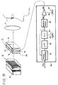
- FIG. 5 shows an apparatus for increasing a resolution in an image display system according to an embodiment of the present invention.
- the apparatus includes an LCD panel 10, an LCD driver 20, an eyepiece 31, an optical path changer 30, and an optical path changer driver 40.
- the LCD panel 10 is combined with a backlight unit BL which applies light from behind the LCD panel 10 to make an image displayed thereon sharper.
- the LCD panel 10 comprises a matrix of pixels 11 each comprising a thin-film transistor (TFT) 11T and a liquid crystal cell 11L.
- the pixels 11 are arranged as shown in FIG. 4A and combined with vertical stripe filters R, G, B each aligned with a vertical column of pixels. Therefore, each vertical column of pixels is associated with one color, i.e., one of the three primaries.
- the LCD panel 10 thus has the arrangement of a color image display system shown in FIGS. 4A through 4C.
- the gates of the thin-film transistors 11T of each horizontal row of pixels indicated by R, G, B, R, B, G, ⁇ are connected in common to each other.
- the gates of the thin-film transistors 11T of the horizontal rows of pixels are connected respectively to row lines Y1, Y2, ⁇ Yj, ⁇ Yn.
- the sources of the thin-film transistors 11T of each vertical column of pixels are connected in common to each other.
- the sources of the thin-film transistors 11T of the vertical columns of pixels are connected respectively to column lines X1, X2, X3, ⁇ Xi, ⁇ Xm.
- the row lines Y1, Y2, ⁇ yj, ⁇ Yn are connected to the respective output terminals of gates 12V1, 12V2, ⁇ 12Vn, which can be opened by a vertical enable signal VEN.
- the gates 12V1, 12V2, ⁇ 12Vn have respective one input terminals connected to respective stages of a vertical shift register 13 which effects vertical scanning.
- the vertical shift register 13 is supplied with a vertical reset pulse VST and vertical clock pulses VCK.
- the vertical shift register 13 successively transfers "1" to effect vertical scanning in response to supplied vertical clock pulses VCK.
- the vertical shift register 13 is reset by the vertical reset pulse VST to determine a phase for starting vertical scanning.
- the column lines X1, X2, ⁇ Xi, ⁇ Xm are connected respectively to signal switches 14H1, 14H2, ⁇ 14Hi, ⁇ 14Hm.
- Those signal switches which are connected to the column lines coupled to the pixel columns of green G are supplied with a green primary signal SG.
- Those signal switches which are connected to the column lines coupled to the pixel columns of blue B are supplied with a blue primary signal SB.
- Those signal switches which are connected to the column lines coupled to the pixel columns of red R are supplied with a red primary signal SR.
- the signal switches 14H1, 14H2, ⁇ 14Hi, ⁇ 14Hm are controlled for their switching operation by respective gates 15H1, 15H2, ⁇ 15Hi, ⁇ 15Hm.
- the gates 15H1, 15H2, ⁇ 15Hi, ⁇ 15Hm have respective one input terminals supplied with a horizontal enable signal HEN which controls these gates 15H1 ⁇ 15Hm for their opening and closing.
- the other input terminals of the gates 15H1 ⁇ 15Hm are supplied with output signals from respective stages of a horizontal shift register 16.
- the horizontal shift register 16 is supplied with a horizontal reset pulse HST and horizontal clock pulses HCK.
- the horizontal shift register 16 is energized by horizontal clock pulses HCK to scan the pixels 11 horizontally to write image information in those pixels that are selected by the vertical scanning.
- the state of a pixel in which image information is stored is maintained for the period of one field.
- the horizontal shift register 16 is reset by the horizontal reset pulse HST to determine a phase for starting horizontal scanning.
- the LCD driver 20 for energizing the LCD panel 10 is illustrated in FIG. 7.
- an NTSC color video signal VI for example, inputted through an input terminal 21 is supplied to an RGB decoder 22 which converts the NTSC color video signal VI into three primary signals VR, VG, VB of red, green, and blue.
- the three primary signals VR, BG, VB are supplied from the RGB decoder 22 to an inverter 23.
- the RGB decoder 22 also extracts a composite synchronizing signal SYNC from the supplied NTSC color video signal VI, and supplies the extracted composite synchronizing signal SYNC to a timing signal generator 24.
- the timing signal generator 24 produces a pulse FRP that is inverted in polarity in each horizontal interval, and supplies the pulse FRP to the inverter 23, which inverts the primary signals VR, BG, VB in each horizontal interval for thereby canceling DC components.
- the inverter 23 supplies primary signals SR, SB, SB which are composed of alternate inverted and noninverted signals in respective horizontal intervals to respective three-primary-signal input terminals 174, 175, 176 of the LCD panel 10 shown in FIG. 6.
- the timing signal generator 24 also generates the horizontal reset pulse HST, the horizontal clock pulses HCK, the horizontal enable signal HEN, the vertical reset pulse VST, the vertical clock pulses VCK, and the vertical enable signal VEN based on the composite synchronizing signal SYNC, and supplies them to respective input terminals 171, 172, 173, 177, 178, 179 of the LCD panel 10 shown in FIG. 6.
- Such image shifting is achieved by switching the horizontal reset pulse HST and the horizontal clock pulses HCK in every field with respect to the horizontal direction and also switching the vertical reset pulse VST and the vertical clock pulses VCK in every field with respect to the vertical direction.
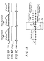
- FIG. 8A shows the color video signal VI inputted through the input terminal 21, the color video signal VI containing a horizontal synchronizing signal HD.
- the horizontal reset pulse HST lags the horizontal synchronizing signal HD by a time to, for example, in an initial period of an effective horizontal video interval.
- the horizontal clock pulses HCK are pulses that repeated in cyclic periods depending on the horizontal pixel pitch PH and the horizontal scanning speed, and are reset by the horizontal reset pulse HST into synchronism with a negative-going edge, for example, of the horizontal reset pulse HST.
- the horizontal reset pulse HST lags the horizontal synchronizing signal HD by a time te.
- FIG. 9A shows one field of the color video signal VI inputted through the input terminal 21, the color video signal VI containing a vertical synchronizing signal VD.
- the vertical reset pulse VST lags the vertical synchronizing signal VD by a time tO in an initial period of an effective vertical video interval.
- the vertical clock pulses VCK are pulses that repeated in cyclic periods depending on the vertical pixel pitch Pv and the vertical scanning speed, and are reset by the vertical reset pulse VST into synchronism with a negative-going edge, for example, of the vertical reset pulse VST.
- the vertical reset pulse VST lags the vertical synchronizing signal VD by a time tE.
- the time tE is longer than the time tO by Pv/2. Since the pixels of the LCD panel 10 start being vertically scanned from the uppermost line (row line Y1) in the vertical direction from the time of the vertical reset pulse VST, images displayed in the odd- and even-numbered fields are vertically shifted from each other by Pv/2.
- the odd- and even-numbered field signals of an interlaced-scanning video signal such as an NTSC color video signal are displayed in positions that are shifted Pv/2 from each other.
- Any signal processing required for shifting a displayed image in the vertical direction remains the same as heretofore, with the vertical reset pulse VST lagging the vertical synchronizing signal VD by a certain time because the vertical synchronizing signal VD being Pv/2 out of phase from field to field.
- images in odd- and even-numbered fields are displayed on the same pixels whose positions remain unchanged apparently.
- images in odd- and even-numbered fields are displayed on pixels whose positions are optically shifted Pv/2 apparently, with the result that the apparent number of pixels is increased for an increased resolution.
- the optical path changer 30 is composed of the eyepiece 31 which comprises a convex lens and a voice coil 32.
- the voice coil 32 when energized, moves the eyepiece 31 linearly in a direction perpendicular to the optical axis of the eyepiece 31 reciprocally in the period of each frame for thereby changing or shifting the optical path through the eyepiece 31 to shift the apparent pixel positions.
- the eyepiece 31 is supported on a lens mount 33 which is vertically vibrated by the voice coil 32 to reciprocally move the eyepiece 31 linearly across the optical axis thereof.
- the voice coil 32 is energized by the optical path changer driver 40.
- the optical path changer driver 40 is supplied with a decision signal O/E (see FIG. 10B) from the LCD driver 20 which indicates whether the present field is an odd-numbered field or an even-numbered field of the color video signal VI (see FIG. 10A).
- the decision signal O/E which has a frequency of 30 Hz, is compared with a signal S43 having a frequency of 30 Hz from a variable-frequency oscillator (hereinafter referred to as a "VCO") 43 by a phase comparator 41.
- a phase error signal S41 outputted from the phase comparator 41 is supplied through a low-pass filter 42 to the VCO 43 to control the output signal S43 thereof into synchronism with the decision signal O/E.
- phase regulator 44 in the form of a variable resistor which adjusts the phase of the output signal S43 with respect to the decision signal O/E into proper phase relationship to the image signal of each field.
- the output signal S43 from the VCO 43 is then supplied to a waveform shaper 45, which produces a rectangular signal.
- the amplitude of the rectangular signal from the waveform shaper 45 is adjusted by a control driver 46 that is associated with an amplitude-adjusting variable resistor 47.
- the control driver 46 supplies an output signal S46 (see FIG. 10C) to the voice coil 32 for thereby energizing the voice coil 32. Specifically, when the signal S46 is of a high level, the eyepiece 31 is moved into a solid-line position in FIG. 11, and when the signal S46 is of a low level, the eyepiece 31 is moved into a dotted-line position in FIG. 11. In this manner, the optical path through the eyepiece 31 is changed or shifted in the period of each field to cause the positions of the pixels of the LCD panel 10 to look shifted optically in the direction perpendicular to the optical axis of the eyepiece 31.
- the resolution is increased most effectively in a central area of the screen of the image display system.
- FIG. 11 shows the principles of an optical shift of the pixel positions, i.e., the changing of an optical path, in the apparatus shown in FIG. 5.
- the eyepiece 31 has a focal length f.
- the image (virtual image) of a point PL that is spaced a distance a from the eyepiece 31, i.e., a displayed image on the LCD panel 10 is focused as a point PO in a position that is spaced a distance b from the eyepiece 31.
- the eyepiece 31 In the even-numbered fields of the video signal VI, the eyepiece 31 is in the dotted-line position which is displaced a distance x upwardly from the solid-line position.
- the image of the point PL as it is observed by the viewer, denoted at 1 in FIG. 5, through the eyepiece 31 is now focused as a point PE in a position that is displaced a distance X downwardly from the point PO. Therefore, the observed image of the point PL is shifted the distance X downwardly.
- the eyepiece 31 When the eyepiece 31 is moved perpendicularly to the optical axis, accordingly, the pixel positions appear to the viewer to be shifted, resulting in an optical shift of the pixel positions.
- the optical pixel shift shown in FIGS. 4A through 4C can be achieved when the eyepiece 31 is shifted by the voice coil 32 in the same direction as the direction of the pixel shift.
- the eyepiece 31 may be combined with a voice coil which can shift the pixels in the horizontal direction of the LCD panel 10 and a voice coil which can shift the pixels in the vertical direction of the LCD panel 10, so that the pixels can optical be shifted in any desired direction under a combination of forces produced by both the voice coils.
- the eyepiece 31 may be reciprocally moved linearly not only by the voice coil, but also by a mechanical device such as a piezoelectric device, a bimorph cell, a stepping motor, a solenoid-operated actuator, or the like.
- a mechanical device such as a piezoelectric device, a bimorph cell, a stepping motor, a solenoid-operated actuator, or the like.
- the apparatus shown in FIG. 5 can easily be realized if the eyepiece 31 is small and light. Since the optical path is changed or shifted in an analog fashion for light deflection, if a reproduced or displayed image is produced by a video camera and suffers a camera shock, then the apparatus shown in FIG. 5 may be used to compensate for such a camera shock by detecting the camera shock based on a displacement of the image.
- the optical pixel shift can be achieved by any of various optical path changers rather than the mechanical vibration of the eyepiece 31.
- FIGS. 12 through 14 show an apparatus for increasing a resolution according to another embodiment of the present invention, the apparatus including a semicircular glass plate as an optical path changer for accomplishing an optical pixel shift.
- the apparatus includes an optical path changer 50 disposed in an optical path between an LCD panel 10 and an eyepiece 31.
- the optical path changer 50 comprises a semicircular glass plate 51 supported by a rigid annular holder 52.
- the annular holder 52 also supports a relatively small segmental counterweight 53 having a weight counterbalancing the semicircular glass plate 51 and positioned radially opposite to the semicircular glass plate 51.
- a hollow bypass region 54 is defined between the semicircular glass plate 51 and the counterweight 53.
- An elongate panel 55 is diametrically attached to the annular holder 52 in intimate contact with a straight side of the semicircular glass plate 51, and connected at its center to a joint 56 which is coupled to the rotatable shaft of a motor 57. Therefore, when the motor 57 is energized, the semicircular glass plate 51 is rotated about the central axis of the annular holder 52.
- the optical path changer 50 is inserted in the optical path between the LCD panel 10 and the eyepiece 31 such that the plane of the semicircular glass plate 51 is inclined to the optical axis of the eye-piece 31.
- the bypass region 54 thereof is positioned in the optical path between the LCD panel 10 and the eyepiece 31.
- the semicircular glass plate 51 is obliquely inserted in the optical path between the LCD panel 10 and the eyepiece 31.
- optical path changer 50 The principles of an optical pixel shift by the optical path changer 50 will be described below with reference to FIG. 14.
- the plane of the semicircular glass plate 51 is inclined an angle ⁇ to a direction perpendicular to the optical axis of the eyepiece 31, the semicircular glass plate 51 has a thickness D and a refractive index n.
- the viewer 1 observes the ray LO of light as coming from a point PLs that is shifted downwardly from the point PL by a distance x, and hence observes pixels as being shifted downwardly by the distance x.
- the motor 57 is energized to rotate the optical path changer 50 at a constant speed to make one revolution in one frame such that the bypass region 54 is positioned in the optical path between the LCD panel 10 and the eyepiece 31 in the odd-numbered fields of a video signal VI supplied to the image display system, and the semicircular glass plate 51 is positioned in the optical path between the LCD panel 10 and the eyepiece 31 in the even-numbered fields of the video signal VI.
- the optical path changer 50 is rotated through one revolution per frame in synchronism with vertical scanning of the LCD panel 10.
- a semicircular outer circumferential surface of the annular holder 52 comprises an optically reflecting surface, and the remaining semicircular outer circumferential surface thereof comprises an optically unreflecting surface.
- An optical rotation phase sensor 58 positioned in confronting relation to the outer circumferential surface of the annular holder 52 comprises a light-emitting element and a light-detecting element. Light emitted from the light-emitting element is applied to the outer circumferential surface of the annular holder 52, and light reflected thereby is detected by the light-detecting element.
- the optical rotation phase sensor 58 is positioned such that it faces the reflecting and non reflecting surfaces of the annular holder 52 substantially in synchronism respectively with even-numbered field intervals in which the semi-circular glass plate 51 is positioned in the optical path between the LCD panel 10 and the eyepiece 31 and odd-numbered field intervals in which the bypass region 54 is positioned in the optical path between the LCD panel 10 and the eyepiece 31.
- a detected output signal S58 (see FIG. 13C) from the optical rotation phase sensor 58 is supplied through an amplifier 59 to a motor driver 60.
- the output signal S58 from the optical rotation phase sensor 58 is compared with a decision signal O/E which indicates whether the present field is an odd-numbered field or an even-numbered field of a supplied video signal VI (see FIG. 13A) by a phase comparator 61.
- a phase error signal outputted from the phase comparator 61 is supplied through a low-pass filter 62 to one input terminal of a differential amplifier 63 whose other input terminal is supplied with a reference voltage REF for establishing a reference phase.
- the reference voltage REF can be adjusted by a variable resistor 64.
- An output signal from the differential amplifier 63 which indicates the voltage of the difference between the signals applied to the input terminals thereof, is supplied through a control driver 65 to the motor 57 for controlling the rotational phase thereof.
- a drive signal applied from the control driver 65 to the motor 57 can be adjusted in amplitude by a variable resistor 66.
- the control loop thus constructed operates until the output signal from the differential amplifier 63 becomes zero whereupon the rotational phase of the optical path changer 50 is synchronized with the decision signal O/E.
- the direction in and the amount by which the pixels are to be optically shifted can be determined by the direction in and the angle through which the semicircular glass plate 51 is inclined with respect to the optical path.
- the apparatus shown in FIGS. 12 through 14 is advantageous in that an optical pixel shift can simply be achieved by rotation of the optical path changer 50 and any vibrational noise which is produced is relatively low.
- FIGS. 15 through 17 show an apparatus for increasing a resolution in an image display system according to still another embodiment of the present invention.
- the apparatus includes an optical path changer 71 comprising a polarization plane rotator 71 and a prismatic birefringent plate 72 made of a material having large birefringence such as quartz, calcite, liquid crystal, or the like.
- the polarization plane rotator 71 comprises a liquid crystal panel 73 and a pair of transparent electrodes 74, 75 mounted on respective opposite surfaces of the liquid crystal panel 73.
- a voltage for driving the liquid crystal is applied between the transparent electrodes 74, 75, the plane of polarization is rotated and changed in every field into conformity with the planes of polarization of ordinary and extraordinary rays of light passing through the birefringent plate 72.
- the polarization plane rotator 71 rotates the plane of polarization between 90° and 0° in every field.
- the voltage for driving the liquid crystal is generated by a driver 80.
- the driver 80 is identical in structure to the driver 40 shown in FIG. 5, and comprises a phase comparator 81, a low-pass filter 82, a VCO 83 associated with a phase corrector 84, a waveform shaper 85, and a control driver 86 associated with an amplitude-adjusting variable resistor 87.
- the VCO 83 produces a signal S83 having the period of frames which is in phase with a decision signal O/E (see FIG. 16B) indicative of whether the present field is an odd-numbered field or an even-numbered field.
- the signal S83 from the VCO 83 is supplied to the waveform shaper 85, which produces a signal S85 having a different amplitude from a voltage S86 (see FIG. 16C) for driving the liquid crystal.
- the signal S85 is then supplied to the control driver 86 and adjusted in amplitude thereby.
- the voltage S86 from the control driver 86 is applied between the transparent electrodes 74, 75 of the polarization plane rotator 71.
- the polarization plane rotator 71 now rotates the plane of polarization from 0° to 90° in the odd-numbered fields, for example, and from 90° to 0° in the even-numbered fields, for example.
- a linearly polarized ray of light which is emitted from an LCD panel 10 is applied to the polarization plane rotator 71, and the plane of polarization thereof is rotated between 0° and 90° in every field. Thereafter, the ray of light enters the birefringent plate 72.
- the amount which the ray of light is deflected is changed due to the difference between the refractive indexes with respect to the ordinary and extraordinary rays of light corresponding to the planes of polarization at 0° and 90°, thus optically shifting a pixel pattern in every field.
- FIG. 17 shows the principles of such an optical pixel shift.
- ⁇ represents a prism angle of the birefringent plate 72
- ⁇ e the angle of refraction of the extraordinary ray of light which is horizontally polarized
- ⁇ o the angle of refraction of the ordinary ray of light is vertically polarized.
- ne is the refractive index with respect to the extraordinary ray of light, no the refractive index with respect to the ordinary ray of light, and * represents a multiplication.
- the birefringent plate 72 is not limited to a prismatic shape, but may be of the type which has a glass plate that is obliquely inserted as shown in FIG. 12, or may comprise a birefringent plate 76 for separating ordinary and extraordinary rays of light at a separation angle ⁇ as shown in FIG. 18.
- the apparatus shown in FIGS. 12 through 18 has a high response speed, can achieve substantially ideal light deflection, and is free from mechanical noise as they deflect light electrically.
- An apparatus for increasing a resolution has an optical path changer in the form of a reflecting mirror as shown in FIG. 19.
- an LCD panel 10 is positioned above and perpendicularly to the optical axis of an eyepiece 31, and has a display surface facing downwardly. Light emitted from the display surface of the LCD panel 10 is reflected toward the eyepiece 31 along the optical axis thereof by a reflecting mirror 91.
- the reflecting mirror 91 is rotatably supported on a support rod 92 which extends parallel to the LCD panel 10. As with the arrangement shown in FIG. 5, the reflecting mirror 91 is coupled through a flexible hinge 95 to an actuating rod 94 which is reciprocally movable vertically in every field by a voice coil 93.
- the voice coil 93 can be energized by a driver 93 which is identical in structure to the driver 40 shown in FIG. 5.
- the reflecting mirror 91 is angularly moved an angle ⁇ in the direction indicated by the arrow about the support rod 92.
- the optical path along which light emitted from the LCD panel 10 is now changed or shifted upwardly from the dotted-line direction to the solid-line direction, thereby effecting an optical pixel shift.
- FIG. 20 shows an apparatus for increasing a resolution in an image display system according to a further embodiment of the present invention.
- an active prism (hereinafter referred to as a "VAP") 100 for use in preventing an image from being displayed due to a camera shock on a camera-combined VTR is employed to change or shift an optical path.
- VAP active prism
- the VAP 100 comprises a liquid having a high refractive index and sealed between two glass panels 101, 102 which are joined to each other by bellows 103.
- One or both of the glass panels 101, 102 can freely be moved vertically and horizontally.
- the VAP 100 is inserted in an optical path between a LCD panel 10 and an eyepiece 31.
- one of the glass panels 102 of the VAP 100 is coupled through a flexible hinge (not shown) to an actuating rod 105 which is reciprocally movable vertically in every field by a voice coil 104.
- the voice coil 104 can be energized by a driver 106 which is identical in structure to the driver 40 shown in FIG. 5.
- the glass panel 102 is changed in its position thereby to change or shift the optical path of light emitted from the LCD panel 10, thus effecting an optical pixel shift.
- FIGS. 21A through 21C show an optical path changer for use in the apparatus shown in FIG. 12.
- an optical path changer 500 comprises seven sectorial glass plates 511 through 517, rather than the semicircular glass plate 51 shown in FIGS. 12 through 14.
- the optical path changer 500 includes a plurality of circumferentially spaced partition plates radially held in an annular holder similar to the annular holder 52 shown in FIG. 12 and dividing a circular space defined by the annular holder into 14 sectorial regions.
- the optical path changer 500 has a joint, similar to the joint 56 shown in FIG. 12, at its center for connection to the rotatable shaft of the motor 57 (see FIG. 12).
- the seven sectorial glass plates 511 through 517 are fitted in every other sectorial regions in the annular holder. Those sectorial regions in which the seven sectorial glass plates 511 through 517 are not fitted serve as bypass regions 540.
- the outer circumferential surface of the annular holder comprise optically reflecting and non reflecting surfaces disposed alternately in angular intervals of 360°/14.
- the optical rotation phase sensor 58 (see FIG. 12) is disposed in confronting relation to the outer circumferential surface of the annular holder. A detected output signal from the rotation phase sensor 58 is supplied to the motor driver 60 (see FIG. 12).
- the optical path changer 500 is obliquely inserted in the optical path between the LCD panel 10 and the viewer.
- the motor driver 60 controls the motor 57 such that the optical path changer 700 makes one revolution in seven frames with each of the sectorial glass plates 511 through 517 appearing in the optical path between the LCD panel 10 and the viewer in an even-numbered field, and also with each of the bypass regions 540 appearing in the optical path between the LCD panel 10 and the viewer in an odd-numbered field.
- the optical path changer 500 can effect an optical pixel shift in the same manner as the apparatus shown in FIG. 12.
- the direction in and the amount by which the pixels are to be optically shifted can be determined by the direction in and the angle through which the sectorial glass plates 511 through 517 are inclined with respect to the optical path.
- the optical path changer 500 makes one revolution in seven frame in synchronism with vertical scanning.
- FIG. 22 shows a polarization plane rotator for use in the apparatus shown in FIG. 15, the polarization plane rotator being a modification of the polarization plane rotator 71 shown in FIG. 15 and serving to shift only one field in synchronism with vertical scanning.
- the polarization plane rotator comprises a liquid crystal panel 73, a transparent electrode 75 mounted on one surface of the liquid crystal panel 73, and an assembly of as many scanning-line electrodes TD (transparent electrodes) which are vertically separate so as to correspond to respective scanning lines as the number of scanning lines, e.g., 218 scanning lines in FIG. 22.
- the scanning-line voltages Ek applied between the scanning-line electrodes and the transparent electrode 75 are shown in FIGS. 23C through 23G.
- the first and second scanning-line electrodes TD1, TD2 serve as an area for writing a present field therein, and the plane of polarization of light passing therethrough is at 90°.
- the third scanning-line electrode TD3 and other scanning-line electrodes positioned therebelow serve as an area for displaying a previous field, and the plane of polarization of light passing therethrough is at 0°.
- one of the transparent electrodes of the polarization plane rotator may not be divided into areas corresponding to the scanning areas, but may be divided into areas corresponding to groups of the scanning lines.
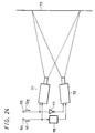
- FIG. 24 shows an apparatus for increasing a resolution in an image display system according to a still further embodiment of the present invention.
- two projectors each having an LCD panel as an image display surface are employed to optically increase the number of pixels used.
- two projectors 111, 112 are directed such that an image projected by the projector 111 and an image projected by the projector 112 are superimposed on a screen 113.
- Each of the projectors 111, 112 has an LCD panel as shown in FIG. 6 and projects an image displayed on the LCD panel onto the screen 113.
- a color video signal VI (see FIG. 25A) is supplied from an input terminal 114 to the projectors 111, 112.
- the supplied color video signal VI is decoded into three-primary signals that are then supplied to the LCD panel.
- a delay circuit 116 for delaying the supplied color video signal by an amount corresponding to the shift of the pixels is inserted in a video signal line connected to the projector 112.
- a decision signal O/E which indicates whether the present field is an odd-numbered field or an even-numbered field of the color video signal VI is supplied as a vertical enable signal VEN to the projector 111.
- the decision signal O/E is inverted by an inverter 117, and supplied as a vertical enable signal VEN to the projector 112.
- the LCD panel In each of the projectors 111, 112, the LCD panel writes image information in the pixels when the vertical enable signal VEN is of an "H” level, and holds the written image information when the vertical enable signal VEN is of an "L” level (LCD noiseless mode).
- the projector 111 displays only odd-numbered fields (see FIG. 25B) and the projector 112 displays only even-numbered fields (see FIG. 25C). If the image projected by the projector 111 is as shown in FIG. 1A, 2A, 3A, or 4A, and the image projected by the projector 112 is as shown in FIG. 1B, 2B, 3B, or 4B, then the combined image displayed on the screen 113 is as shown in FIG. 1C, 2C, 3C, or 4C.
- an image signal for a left eye is supplied as odd-numbered fields to the projector 111 and an image signal for a right eye is supplied as even-numbered fields to the projector 112, and the planes of polarization of rays of light that are projected by the respective projectors 111, 112 lie perpendicularly to each other, then a three-dimensional image can be observed on the screen 113 by the viewer using polarized glasses.
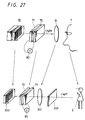
- the LCD panel 10 may be replaced with a CCD imaging unit 200, the viewer 1 with a subject 2, and the eyepiece 31 with an objective 201, with light traveling in the opposite direction, and the optical path may be changed or shifted in the manner described above, for increasing the resolution of an image that is produced by an imaging apparatus such as a CCD camera.
- FIG. 26 shows a CCD camera which corresponds to the arrangement shown in FIG. 5.
- FIG. 27 shows a CCD camera which corresponds to the arrangement shown in FIGS. 15 through 17.
- the polarization plane rotator 71 and the birefringent plate 72 are switched around because the light travels in the opposite direction.
- the polarization plane rotator 71 and the birefringent plate 72 may be positioned between the objective 2 and the objective 201.
- the number of pixels of the CCD imaging unit is selected to match the interlaced scanning of video signals. Therefore, all the pixels of the CCD imaging unit may be handled as the pixels of one field, and the pixels may be optically shifted vertically in the manner described above to apparently make the number of horizontal scanning lines twice that of NTSC signals, thereby producing an image signal according to high-definition television (HDTV) standards.
- HDTV high-definition television
- Still images which are not required to be shifted in every field may be processed using an optical deflector such as a VAP.
- an optical deflector such as a VAP.
- Still images having a high resolution may be outputted using a printer or displayed on a HDTV monitor.
- FIG. 28 shows, in block form, a recording and reproducing apparatus according to the present invention, with a camera combined therewith.
- the recording and reproducing apparatus can record still images of high resolution with a CCD camera shown in FIG. 26 or 27 and also reproduce recorded still images.
- the optical path of light from a subject 2 is optically shifted vertically and/or horizontally a predetermined amount in synchronism with a field or a frame by an optical path changer 210 including an imaging optical system, and then the light is applied to a CCD imaging unit 200.
- a shutter mechanism SHT is disposed between the CCD imaging unit 200 and the subject 2.
- the shutter mechanism SHT is opened during at least one cycle of an optical path shift because the recording and reproducing apparatus shown in FIG. 28 produces a combined high-resolution still image by combining field images of a subject (still image) that are sampled at spatially different positions by the optical path shift.
- the optical path is shifted by the optical path changer 210 in a direction and by an amount depending on a drive signal applied from a driver 211 to the optical path changer 210.
- the CCD imaging unit 200 generates an image signal that is outputted in response to a timing signal from an output reader 212.
- the output reader 212 is supplied with a shift timing signal from the driver 211 such that the image signal is read from the CCD imaging unit 200 in synchronism with the shifting of the optical path.
- the image signal from the CCD imaging unit 200 is supplied to an image signal processor 213, which processes the image signal into a color video signal supplied to a recording signal processor 214.
- the recording signal processor 214 processes, e.g., modulates, the color video signal.
- a change quantity and direction information generator 215 produces information ID representing the quantity and direction of an optical path shift effected by the optical path changer 210, based on a signal from the driver 211, and supplies the information ID to the recording signal processor 214.
- the information ID also contains information indicative of now many field images are to be combined into a combined high-resolution still image.
- the recording signal processor 214 inserts or adds the information ID in or to a period, such as a vertical blanking period of a color video signal to be recorded, other than a main signal interval.
- An output signal from the recording signal processor 214 is supplied through a recording contact R of a recording/playback selector switch 216 to a rotary head, which records the signal on a magnetic tape.
- a recorded signal is reproduced as follows:
- a signal reproduced from the magnetic tape by the rotary head is supplied through a reproducing contact P of the recording/playback selector switch 216 to a reproduced signal processor 221.
- the reproduced signal processor 221 demodulates a color video signal from the reproduced signal, and supplies the demodulated color video signal to an image restorer and combiner 222.
- the reproduced signal processor 221 also extracts information ID from the reproduced signal, and supplies the extracted information ID to a change quantity and direction information reproducer 223.
- the change quantity and direction information reproducer 223 reproduces information representing the number of field images to be combined into a single still image and the quantity and direction of an optical path shift of each of the field images, and supplies the reproduced information to the image restorer and combiner 222.
- the image restorer and combiner 222 has a frame memory which stores a digital color video signal that has been converted from the analog color video signal from the reproduced signal processor 221.
- the digital color video signal read from the frame memory of the image restorer and combiner 222 is converted into an analog color video signal, which is supplied to a display monitor 224 or a printer 225.
- the printer 225 may be supplied with the digital color video signal directly.
- the frame memory of the image restorer and combiner 222 comprises a memory that can store more pixels than the pixels that are sampled in the analog-to-digital and digital-to-analog conversions per field. Stated otherwise, the frame memory is capable of a number of pixels corresponding to the maximum number of field images that are to be combined with each other.
- the image restorer and combiner 222 Based on the information as to the quantity and direction of an optical path shift from the change quantity and direction information reproducer 223, the image restorer and combiner 222 writes each of the field images which will constitute a still image into the frame memory so as to correspond to their spatially sampled positions at the time the field image is produced.
- the frame memory stores the information of a still image having a greater resolution than the resolution of the CCD imaging unit 200.
- the still image information stored in the frame memory is converted into analog information, which is supplied to the display monitor 224 for display or to the printer 225 for printout as a hard copy. If the display monitor 224 or the printer 225 can display or print high-resolution images, then a still image of high resolution can be displayed or printed. If the display monitor 224 or the printer 225 is of low resolution, then the still image information stored in the frame memory is decimated and supplied to the display monitor 224 or the printer 225.
- the recording and reproducing apparatus shown in FIG. 28 employs an interlaced-scanning full-line imaging unit as the CCD imaging unit 200, and combines a plurality of field images that have been produced by effecting an optical path shift horizontally and vertically into a still image of high resolution. If the optical path shift is carried out in smaller steps in the horizontal and vertical directions, thus producing more field images to be combined, the number of pixels is increased by the number of field images to be combined, so that a combined still image having a resolution that is more than twice that of ordinary interlaced-scanning images can be produced.
- the recording and reproducing apparatus may be divided into an imaging and recording apparatus and a reproducing apparatus which are separate from each other.
- the image signal from the recording signal processor 214 may be recorded on not only the magnetic tape but also an optical disk, an IC memory, an IC card, or any of various other information storage mediums.
- the information ID representing an optical path shift may be recorded in a recording area separate from the video signal in relation thereto, rather than being added to the vertical blanking interval of the video signal.
- an optical path between an image display panel and the viewer or screen is changed or shifted in every field of a video signal for optically deflecting or shifting pixels, and the image display panel displays images that are shifted due to the optically shifted pixels.
- Noninterlaced full-line images can be displayed and observed for higher resolution without having to increase the number of pixels of the image display panel.
- the image display panel can display images with high brightness.
- high-resolution images can be displayed on inexpensive image display panels having a relatively small number of pixels.
- the total number of pixels may be four or more times the number of original pixels of the image display panel.
- the principles of the present invention are applied to an image display system having a number of pixels capable of displaying NTSC video signals according to the noninterlaced scanning process, then it can display an image based on a HDTV signal characterized by 1125 scanning lines.
- the present invention which allows high-resolution images to be displayed on inexpensive image display panels is applicable to a wide variety of display devices including an electronic viewfinder for an imaging camera, a projector, a glass-type monitor, etc.
- the method of increasing the resolution of an image according to the present invention can be employed in an imaging camera or the like.
- FIGS. 12 and 21 can achieve an optical path shift simply by effecting rotational movements without producing large vibrational noise.
- FIGS. 15 and 22 have a high response speed, can achieve substantially ideal light deflection, and is free from mechanical noise as they deflect light electrically.
Applications Claiming Priority (4)
| Application Number | Priority Date | Filing Date | Title |
|---|---|---|---|
| JP16955/93 | 1993-01-07 | ||
| JP1695593 | 1993-01-07 | ||
| JP19697393A JP3547015B2 (ja) | 1993-01-07 | 1993-07-14 | 画像表示装置および画像表示装置の解像度改善方法 |
| JP196973/93 | 1993-07-14 |
Publications (3)
| Publication Number | Publication Date |
|---|---|
| EP0606162A2 true EP0606162A2 (de) | 1994-07-13 |
| EP0606162A3 EP0606162A3 (de) | 1994-11-02 |
| EP0606162B1 EP0606162B1 (de) | 1998-11-11 |
Family
ID=26353409
Family Applications (1)
| Application Number | Title | Priority Date | Filing Date |
|---|---|---|---|
| EP94300080A Expired - Lifetime EP0606162B1 (de) | 1993-01-07 | 1994-01-06 | Bildanzeigesystem mit Mosaikmustern aus Pixeln |
Country Status (4)
| Country | Link |
|---|---|
| US (1) | US5689283A (de) |
| EP (1) | EP0606162B1 (de) |
| JP (1) | JP3547015B2 (de) |
| DE (1) | DE69414427T2 (de) |
Cited By (22)
| Publication number | Priority date | Publication date | Assignee | Title |
|---|---|---|---|---|
| EP0723174A2 (de) * | 1995-01-17 | 1996-07-24 | International Business Machines Corporation | Farbteiler mit drei Prismen |
| EP0751683A2 (de) * | 1995-06-30 | 1997-01-02 | Victor Company Of Japan Limited | Bildverarbeitungs-, -anzeige- und -aufnahmevorrichtung |
| EP0789852A1 (de) * | 1994-10-25 | 1997-08-20 | James L. Fergason | Optisches anzeigesystem und -verfahren, aktives und passives halbtonverfahren unter benutzung der doppelbrechung, überlagerung von farbbildern sowie bildverbesserung |
| EP0794676A2 (de) * | 1996-03-09 | 1997-09-10 | Koninklijke Philips Electronics N.V. | Zeilensprung-Bildprojektor |
| EP0887681A2 (de) * | 1997-06-26 | 1998-12-30 | Xerox Corporation | Fehler-unempfindliche Projektions-Anzeige mit redundanten Lichtmodulatoren |
| WO1999025161A2 (en) * | 1997-11-11 | 1999-05-20 | Anatoly Ivanov | Methods and devices for picking up/displaying images |
| EP0951185A1 (de) * | 1998-04-13 | 1999-10-20 | Olympus Optical Co., Ltd. | Bildanzeigevorrichtung |
| EP1001306A2 (de) * | 1998-11-12 | 2000-05-17 | Olympus Optical Co., Ltd. | Bildanzeigevorrichtung |
| US6184969B1 (en) | 1994-10-25 | 2001-02-06 | James L. Fergason | Optical display system and method, active and passive dithering using birefringence, color image superpositioning and display enhancement |
| US6243055B1 (en) | 1994-10-25 | 2001-06-05 | James L. Fergason | Optical display system and method with optical shifting of pixel position including conversion of pixel layout to form delta to stripe pattern by time base multiplexing |
| WO2001069942A2 (en) * | 2000-03-15 | 2001-09-20 | Imax Corporation | Methods and apparatuses for superimposition of images |
| US6751006B2 (en) | 2000-07-03 | 2004-06-15 | Imax Corporation | Processing techniques for superimposing images for image projection |
| US6919990B2 (en) | 2000-04-18 | 2005-07-19 | Imax Corporation | Methods and systems for low loss separation and combination of light |
| WO2005067307A1 (en) * | 2003-12-23 | 2005-07-21 | 3M Innovative Properties Company | Pixel-shifting projection lens assembly to provide optical interlacing for increased addressability |
| US7046407B2 (en) | 2000-02-14 | 2006-05-16 | 3M Innovative Properties Company | Diffractive color filter |
| US7113231B2 (en) | 2000-02-14 | 2006-09-26 | 3M Innovative Properties Company | Dot-sequential color display system |
| US7193654B2 (en) | 2000-07-03 | 2007-03-20 | Imax Corporation | Equipment and techniques for invisible seaming of multiple projection displays |
| US7224411B2 (en) | 2000-03-31 | 2007-05-29 | Imax Corporation | Digital projection equipment and techniques |
| US7224335B2 (en) | 2000-03-15 | 2007-05-29 | Imax Corporation | DMD-based image display systems |
| US8243004B2 (en) | 2003-03-10 | 2012-08-14 | Fergason Patent Properties, Llc | Apparatus and method for preparing, storing, transmitting and displaying images |
| US8251512B2 (en) | 2004-07-08 | 2012-08-28 | Imax Corporation | Equipment and methods for the display of high resolution images using multiple projection displays |
| WO2020167374A1 (en) | 2019-02-16 | 2020-08-20 | Leia Inc. | Multiview display and method having light control film |
Families Citing this family (171)
| Publication number | Priority date | Publication date | Assignee | Title |
|---|---|---|---|---|
| JPH08194207A (ja) * | 1995-01-20 | 1996-07-30 | Olympus Optical Co Ltd | 画像表示装置 |
| US6061103A (en) * | 1995-01-20 | 2000-05-09 | Olympus Optical Co., Ltd. | Image display apparatus |
| JPH09322099A (ja) * | 1996-05-30 | 1997-12-12 | Olympus Optical Co Ltd | 映像表示装置 |
| US6559825B2 (en) | 1996-10-31 | 2003-05-06 | Kopin Corporation | Display system for wireless pager |
| US6545654B2 (en) | 1996-10-31 | 2003-04-08 | Kopin Corporation | Microdisplay for portable communication systems |
| US6486862B1 (en) * | 1996-10-31 | 2002-11-26 | Kopin Corporation | Card reader display system |
| US6677936B2 (en) | 1996-10-31 | 2004-01-13 | Kopin Corporation | Color display system for a camera |
| JPH10186313A (ja) * | 1996-12-25 | 1998-07-14 | Furontetsuku:Kk | カラー液晶表示装置 |
| JP3560756B2 (ja) * | 1997-02-13 | 2004-09-02 | アルプス電気株式会社 | 表示装置の駆動方法 |
| KR19990009016A (ko) * | 1997-07-07 | 1999-02-05 | 윤종용 | 복굴절 물질을 이용한 레이저 투사 영상 장치 및 방법 |
| US6104375A (en) * | 1997-11-07 | 2000-08-15 | Datascope Investment Corp. | Method and device for enhancing the resolution of color flat panel displays and cathode ray tube displays |
| JP3926922B2 (ja) * | 1998-03-23 | 2007-06-06 | オリンパス株式会社 | 画像表示装置 |
| JP3934250B2 (ja) | 1998-05-11 | 2007-06-20 | オリンパス株式会社 | 画像表示装置 |
| JP4101943B2 (ja) | 1998-08-07 | 2008-06-18 | オリンパス株式会社 | 画像表示装置 |
| US6307566B1 (en) | 1998-10-07 | 2001-10-23 | Microsoft Corporation | Methods and apparatus for performing image rendering and rasterization operations |
| US6356278B1 (en) | 1998-10-07 | 2002-03-12 | Microsoft Corporation | Methods and systems for asymmeteric supersampling rasterization of image data |
| US6278434B1 (en) | 1998-10-07 | 2001-08-21 | Microsoft Corporation | Non-square scaling of image data to be mapped to pixel sub-components |
| US6236390B1 (en) | 1998-10-07 | 2001-05-22 | Microsoft Corporation | Methods and apparatus for positioning displayed characters |
| US6188385B1 (en) | 1998-10-07 | 2001-02-13 | Microsoft Corporation | Method and apparatus for displaying images such as text |
| JP5231697B2 (ja) * | 1998-10-07 | 2013-07-10 | マイクロソフト コーポレーション | 表示される画像の解像度を改善する方法およびコンピュータ・システム |
| US6225973B1 (en) | 1998-10-07 | 2001-05-01 | Microsoft Corporation | Mapping samples of foreground/background color image data to pixel sub-components |
| US6597360B1 (en) * | 1998-10-07 | 2003-07-22 | Microsoft Corporation | Automatic optimization of the position of stems of text characters |
| JP4103216B2 (ja) * | 1998-12-09 | 2008-06-18 | ノーリツ鋼機株式会社 | 写真焼付装置 |
| US6393145B2 (en) | 1999-01-12 | 2002-05-21 | Microsoft Corporation | Methods apparatus and data structures for enhancing the resolution of images to be rendered on patterned display devices |
| US6973210B1 (en) | 1999-01-12 | 2005-12-06 | Microsoft Corporation | Filtering image data to obtain samples mapped to pixel sub-components of a display device |
| US6750875B1 (en) | 1999-02-01 | 2004-06-15 | Microsoft Corporation | Compression of image data associated with two-dimensional arrays of pixel sub-components |
| US6674436B1 (en) | 1999-02-01 | 2004-01-06 | Microsoft Corporation | Methods and apparatus for improving the quality of displayed images through the use of display device and display condition information |
| US7134091B2 (en) * | 1999-02-01 | 2006-11-07 | Microsoft Corporation | Quality of displayed images with user preference information |
| US6342890B1 (en) | 1999-03-19 | 2002-01-29 | Microsoft Corporation | Methods, apparatus, and data structures for accessing sub-pixel data having left side bearing information |
| US6342896B1 (en) * | 1999-03-19 | 2002-01-29 | Microsoft Corporation | Methods and apparatus for efficiently implementing and modifying foreground and background color selections |
| US6339426B1 (en) | 1999-04-29 | 2002-01-15 | Microsoft Corporation | Methods, apparatus and data structures for overscaling or oversampling character feature information in a system for rendering text on horizontally striped displays |
| US6657603B1 (en) * | 1999-05-28 | 2003-12-02 | Lasergraphics, Inc. | Projector with circulating pixels driven by line-refresh-coordinated digital images |
| US6282327B1 (en) | 1999-07-30 | 2001-08-28 | Microsoft Corporation | Maintaining advance widths of existing characters that have been resolution enhanced |
| US6226017B1 (en) | 1999-07-30 | 2001-05-01 | Microsoft Corporation | Methods and apparatus for improving read/modify/write operations |
| US6738526B1 (en) | 1999-07-30 | 2004-05-18 | Microsoft Corporation | Method and apparatus for filtering and caching data representing images |
| JP3967500B2 (ja) * | 1999-09-08 | 2007-08-29 | 富士フイルム株式会社 | 固体撮像装置および信号読出し方法 |
| JP4474000B2 (ja) | 2000-01-20 | 2010-06-02 | キヤノン株式会社 | 投影装置 |
| US20030020809A1 (en) * | 2000-03-15 | 2003-01-30 | Gibbon Michael A | Methods and apparatuses for superimposition of images |
| US6997532B2 (en) * | 2000-12-22 | 2006-02-14 | Polaroid Corporation | Digital image printer and method |
| US7339714B1 (en) | 2001-02-02 | 2008-03-04 | Cheetah Omni, Llc | Variable blazed grating based signal processing |
| JP2002268014A (ja) | 2001-03-13 | 2002-09-18 | Olympus Optical Co Ltd | 画像表示装置 |
| JP3956337B2 (ja) | 2001-03-16 | 2007-08-08 | オリンパス株式会社 | 面順次カラー表示装置 |
| US7307646B2 (en) * | 2001-05-09 | 2007-12-11 | Clairvoyante, Inc | Color display pixel arrangements and addressing means |
| JP4913291B2 (ja) * | 2001-05-30 | 2012-04-11 | 株式会社リコー | 表示装置および画像投射装置 |
| US7064740B2 (en) | 2001-11-09 | 2006-06-20 | Sharp Laboratories Of America, Inc. | Backlit display with improved dynamic range |
| US7030845B2 (en) * | 2002-01-20 | 2006-04-18 | Shalong Maa | Digital enhancement of streaming video and multimedia system |
| US7125121B2 (en) | 2002-02-25 | 2006-10-24 | Ricoh Company, Ltd. | Image display apparatus |
| JP4537664B2 (ja) | 2002-04-17 | 2010-09-01 | 株式会社リコー | 光路偏向素子、光路偏向装置、画像表示装置、光書込み装置、光インターコネクション装置、光学素子及びその製造方法 |
| KR100884993B1 (ko) * | 2002-04-20 | 2009-02-20 | 엘지디스플레이 주식회사 | 액정표시장치 및 그 구동방법 |
| US7038835B2 (en) | 2002-05-28 | 2006-05-02 | Ricoh Company, Ltd. | Optical deflection device and optical deflection method that control occurrence of alignment defect |
| JP2004021098A (ja) * | 2002-06-19 | 2004-01-22 | Ricoh Co Ltd | 光路偏向デバイス及び画像表示装置 |
| US7030894B2 (en) * | 2002-08-07 | 2006-04-18 | Hewlett-Packard Development Company, L.P. | Image display system and method |
| US7034811B2 (en) | 2002-08-07 | 2006-04-25 | Hewlett-Packard Development Company, L.P. | Image display system and method |
| US7172288B2 (en) * | 2003-07-31 | 2007-02-06 | Hewlett-Packard Development Company, L.P. | Display device including a spatial light modulator with plural image regions |
| US7317465B2 (en) * | 2002-08-07 | 2008-01-08 | Hewlett-Packard Development Company, L.P. | Image display system and method |
| US6963319B2 (en) * | 2002-08-07 | 2005-11-08 | Hewlett-Packard Development Company, L.P. | Image display system and method |
| US20060007406A1 (en) * | 2002-10-21 | 2006-01-12 | Sean Adkins | Equipment, systems and methods for control of color in projection displays |
| JP2004266808A (ja) * | 2003-02-10 | 2004-09-24 | Sony Corp | 画像処理装置および画像処理方法、画像表示システム、記録媒体、並びにプログラム |
| JP4620933B2 (ja) * | 2003-02-24 | 2011-01-26 | 株式会社リコー | 情報表示装置 |
| US7098936B2 (en) * | 2003-03-11 | 2006-08-29 | Hewlett-Packard Development Company, L.P. | Image display system and method including optical scaling |
| US7245430B2 (en) | 2003-04-21 | 2007-07-17 | Ricoh Company, Ltd. | Method and apparatus for displaying three-dimensional stereo image using light deflector |
| JP4161814B2 (ja) | 2003-06-16 | 2008-10-08 | ソニー株式会社 | 入力方法および入力装置 |
| US7289114B2 (en) * | 2003-07-31 | 2007-10-30 | Hewlett-Packard Development Company, L.P. | Generating and displaying spatially offset sub-frames |
| US7109981B2 (en) | 2003-07-31 | 2006-09-19 | Hewlett-Packard Development Company, L.P. | Generating and displaying spatially offset sub-frames |
| US7253811B2 (en) * | 2003-09-26 | 2007-08-07 | Hewlett-Packard Development Company, L.P. | Generating and displaying spatially offset sub-frames |
| US7190380B2 (en) * | 2003-09-26 | 2007-03-13 | Hewlett-Packard Development Company, L.P. | Generating and displaying spatially offset sub-frames |
| JP4839218B2 (ja) * | 2003-10-16 | 2011-12-21 | トムソン ライセンシング | ピクセルシフトカラー投射システム |
| US7301549B2 (en) * | 2003-10-30 | 2007-11-27 | Hewlett-Packard Development Company, L.P. | Generating and displaying spatially offset sub-frames on a diamond grid |
| US20050093894A1 (en) * | 2003-10-30 | 2005-05-05 | Tretter Daniel R. | Generating an displaying spatially offset sub-frames on different types of grids |
| US7330181B2 (en) | 2003-10-31 | 2008-02-12 | Sony Corporation | Method and apparatus for processing an image, image display system, storage medium, and program |
| JP4337505B2 (ja) | 2003-10-31 | 2009-09-30 | ソニー株式会社 | 撮像装置および撮像方法、画像処理装置および画像処理方法、画像表示システム、記録媒体、並びにプログラム |
| JP4488337B2 (ja) * | 2003-11-21 | 2010-06-23 | 株式会社リコー | 表示装置 |
| US7414595B1 (en) | 2003-12-07 | 2008-08-19 | Advanced Simulation Displays Co. | Virtual mosaic wide field of view display system |
| US7660487B2 (en) | 2003-12-10 | 2010-02-09 | Sony Corporation | Image processing method and apparatus with image resolution conversion related to relative movement detection |
| US7164284B2 (en) | 2003-12-18 | 2007-01-16 | Sharp Laboratories Of America, Inc. | Dynamic gamma for a liquid crystal display |
| KR20050069828A (ko) * | 2003-12-31 | 2005-07-05 | 엘지전자 주식회사 | 고해상도 투사 장치 |
| US7355612B2 (en) * | 2003-12-31 | 2008-04-08 | Hewlett-Packard Development Company, L.P. | Displaying spatially offset sub-frames with a display device having a set of defective display pixels |
| US7086736B2 (en) * | 2004-01-20 | 2006-08-08 | Hewlett-Packard Development Company, L.P. | Display system with sequential color and wobble device |
| US6984040B2 (en) * | 2004-01-20 | 2006-01-10 | Hewlett-Packard Development Company, L.P. | Synchronizing periodic variation of a plurality of colors of light and projection of a plurality of sub-frame images |
| US7463272B2 (en) * | 2004-01-30 | 2008-12-09 | Hewlett-Packard Development Company, L.P. | Generating and displaying spatially offset sub-frames |
| US7483044B2 (en) * | 2004-01-30 | 2009-01-27 | Hewlett-Packard Development Company, L.P. | Displaying sub-frames at spatially offset positions on a circle |
| US7629989B2 (en) * | 2004-04-02 | 2009-12-08 | K-Nfb Reading Technology, Inc. | Reducing processing latency in optical character recognition for portable reading machine |
| US20050225570A1 (en) * | 2004-04-08 | 2005-10-13 | Collins David C | Generating and displaying spatially offset sub-frames |
| US7660485B2 (en) * | 2004-04-08 | 2010-02-09 | Hewlett-Packard Development Company, L.P. | Generating and displaying spatially offset sub-frames using error values |
| US20050225571A1 (en) * | 2004-04-08 | 2005-10-13 | Collins David C | Generating and displaying spatially offset sub-frames |
| JP4884652B2 (ja) * | 2004-04-16 | 2012-02-29 | 株式会社リコー | 画像表示/画像取込み装置および画像表示/画像取込み方法 |
| US7023449B2 (en) * | 2004-04-30 | 2006-04-04 | Hewlett-Packard Development Company, L.P. | Displaying least significant color image bit-planes in less than all image sub-frame locations |
| US7777714B2 (en) | 2004-05-04 | 2010-08-17 | Sharp Laboratories Of America, Inc. | Liquid crystal display with adaptive width |
| US8395577B2 (en) | 2004-05-04 | 2013-03-12 | Sharp Laboratories Of America, Inc. | Liquid crystal display with illumination control |
| US7872631B2 (en) | 2004-05-04 | 2011-01-18 | Sharp Laboratories Of America, Inc. | Liquid crystal display with temporal black point |
| US7657118B2 (en) * | 2004-06-09 | 2010-02-02 | Hewlett-Packard Development Company, L.P. | Generating and displaying spatially offset sub-frames using image data converted from a different color space |
| US7023451B2 (en) | 2004-06-14 | 2006-04-04 | Sharp Laboratories Of America, Inc. | System for reducing crosstalk |
| US7668398B2 (en) * | 2004-06-15 | 2010-02-23 | Hewlett-Packard Development Company, L.P. | Generating and displaying spatially offset sub-frames using image data with a portion converted to zero values |
| US20050275669A1 (en) * | 2004-06-15 | 2005-12-15 | Collins David C | Generating and displaying spatially offset sub-frames |
| US7453478B2 (en) * | 2004-07-29 | 2008-11-18 | Hewlett-Packard Development Company, L.P. | Address generation in a light modulator |
| US7522177B2 (en) * | 2004-09-01 | 2009-04-21 | Hewlett-Packard Development Company, L.P. | Image display system and method |
| US7453449B2 (en) * | 2004-09-23 | 2008-11-18 | Hewlett-Packard Development Company, L.P. | System and method for correcting defective pixels of a display device |
| US7898519B2 (en) | 2005-02-17 | 2011-03-01 | Sharp Laboratories Of America, Inc. | Method for overdriving a backlit display |
| US7474319B2 (en) * | 2004-10-20 | 2009-01-06 | Hewlett-Packard Development Company, L.P. | Generating and displaying spatially offset sub-frames |
| US7267442B2 (en) * | 2004-10-20 | 2007-09-11 | Hewlett-Packard Development Company, L.P. | Pixelated color wobulation |
| US8050511B2 (en) | 2004-11-16 | 2011-11-01 | Sharp Laboratories Of America, Inc. | High dynamic range images from low dynamic range images |
| US8050512B2 (en) | 2004-11-16 | 2011-11-01 | Sharp Laboratories Of America, Inc. | High dynamic range images from low dynamic range images |
| US7676113B2 (en) * | 2004-11-19 | 2010-03-09 | Hewlett-Packard Development Company, L.P. | Generating and displaying spatially offset sub-frames using a sharpening factor |
| US8872869B2 (en) * | 2004-11-23 | 2014-10-28 | Hewlett-Packard Development Company, L.P. | System and method for correcting defective pixels of a display device |
| JP4672343B2 (ja) * | 2004-11-25 | 2011-04-20 | 株式会社リコー | 画像表示装置 |
| JP4751619B2 (ja) | 2005-01-31 | 2011-08-17 | 株式会社リコー | 中間結像光学系、それを用いた画像表示装置、および中間結像光学系に用いられる電圧印加方法 |
| US7661810B2 (en) * | 2005-03-02 | 2010-02-16 | Fujifilm Corporation | Image recording apparatus and inkjet apparatus for double-side recording |
| US7443364B2 (en) * | 2005-03-15 | 2008-10-28 | Hewlett-Packard Development Company, L.P. | Projection of overlapping sub-frames onto a surface |
| US7466291B2 (en) * | 2005-03-15 | 2008-12-16 | Niranjan Damera-Venkata | Projection of overlapping single-color sub-frames onto a surface |
| US9282335B2 (en) | 2005-03-15 | 2016-03-08 | Hewlett-Packard Development Company, L.P. | System and method for coding image frames |
| US7489383B2 (en) | 2005-04-22 | 2009-02-10 | Ricoh Company, Ltd. | Optical axis deflecting method, optical axis deflecting element, optical path deflecting unit, method of driving optical axis deflecting element, and image display apparatus |
| US7407295B2 (en) * | 2005-07-26 | 2008-08-05 | Niranjan Damera-Venkata | Projection of overlapping sub-frames onto a surface using light sources with different spectral distributions |
| US7387392B2 (en) * | 2005-09-06 | 2008-06-17 | Simon Widdowson | System and method for projecting sub-frames onto a surface |
| US20070076171A1 (en) * | 2005-09-20 | 2007-04-05 | Fasen Donald J | Wobulator position sensing system and method |
| US20070091277A1 (en) * | 2005-10-26 | 2007-04-26 | Niranjan Damera-Venkata | Luminance based multiple projector system |
| US7470032B2 (en) * | 2005-10-27 | 2008-12-30 | Hewlett-Packard Development Company, L.P. | Projection of overlapping and temporally offset sub-frames onto a surface |
| US20070097017A1 (en) * | 2005-11-02 | 2007-05-03 | Simon Widdowson | Generating single-color sub-frames for projection |
| US20070133794A1 (en) * | 2005-12-09 | 2007-06-14 | Cloutier Frank L | Projection of overlapping sub-frames onto a surface |
| US20070132967A1 (en) * | 2005-12-09 | 2007-06-14 | Niranjan Damera-Venkata | Generation of image data subsets |
| US20070133087A1 (en) * | 2005-12-09 | 2007-06-14 | Simon Widdowson | Generation of image data subsets |
| US7559661B2 (en) | 2005-12-09 | 2009-07-14 | Hewlett-Packard Development Company, L.P. | Image analysis for generation of image data subsets |
| US20070132965A1 (en) * | 2005-12-12 | 2007-06-14 | Niranjan Damera-Venkata | System and method for displaying an image |
| US8356905B2 (en) * | 2005-12-21 | 2013-01-22 | Parellel Consulting Limited Liability Company | Optically enhanced image sequences |
| US8121401B2 (en) | 2006-01-24 | 2012-02-21 | Sharp Labortories of America, Inc. | Method for reducing enhancement of artifacts and noise in image color enhancement |
| US9143657B2 (en) | 2006-01-24 | 2015-09-22 | Sharp Laboratories Of America, Inc. | Color enhancement technique using skin color detection |
| KR100761438B1 (ko) * | 2006-02-27 | 2007-09-27 | 이영화 | 근접 대상물의 입체동영상을 촬영하기 위한입체동영상촬영장치 |
| EP1989276A4 (de) | 2006-03-01 | 2011-03-02 | Ricoh Co Ltd | Flüssigkristallelement, den lichtweg umlenkendes elementen und bildanzeigevorrichtung |
| JP4799225B2 (ja) * | 2006-03-08 | 2011-10-26 | 株式会社東芝 | 画像処理装置および画像表示方法 |
| US7499214B2 (en) * | 2006-03-20 | 2009-03-03 | Hewlett-Packard Development Company, L.P. | Ambient light absorbing screen |
| US20070291184A1 (en) * | 2006-06-16 | 2007-12-20 | Michael Harville | System and method for displaying images |
| US7854518B2 (en) * | 2006-06-16 | 2010-12-21 | Hewlett-Packard Development Company, L.P. | Mesh for rendering an image frame |
| US9137504B2 (en) | 2006-06-16 | 2015-09-15 | Hewlett-Packard Development Company, L.P. | System and method for projecting multiple image streams |
| US7907792B2 (en) | 2006-06-16 | 2011-03-15 | Hewlett-Packard Development Company, L.P. | Blend maps for rendering an image frame |
| US7800628B2 (en) * | 2006-06-16 | 2010-09-21 | Hewlett-Packard Development Company, L.P. | System and method for generating scale maps |
| US20080002160A1 (en) * | 2006-06-30 | 2008-01-03 | Nelson Liang An Chang | System and method for generating and displaying sub-frames with a multi-projector system |
| US20080024389A1 (en) * | 2006-07-27 | 2008-01-31 | O'brien-Strain Eamonn | Generation, transmission, and display of sub-frames |
| US20080024469A1 (en) * | 2006-07-31 | 2008-01-31 | Niranjan Damera-Venkata | Generating sub-frames for projection based on map values generated from at least one training image |
| US20080024683A1 (en) * | 2006-07-31 | 2008-01-31 | Niranjan Damera-Venkata | Overlapped multi-projector system with dithering |
| EP2051134A4 (de) | 2006-08-09 | 2010-09-22 | Sharp Kk | Flüssigkristallanzeigeanordnung und betrachtungswinkel-steuermodul |
| US20080043209A1 (en) * | 2006-08-18 | 2008-02-21 | Simon Widdowson | Image display system with channel selection device |
| US20080095363A1 (en) * | 2006-10-23 | 2008-04-24 | Dicarto Jeffrey M | System and method for causing distortion in captured images |
| US20080094419A1 (en) * | 2006-10-24 | 2008-04-24 | Leigh Stan E | Generating and displaying spatially offset sub-frames |
| US20080101711A1 (en) * | 2006-10-26 | 2008-05-01 | Antonius Kalker | Rendering engine for forming an unwarped reproduction of stored content from warped content |
| US20080101725A1 (en) * | 2006-10-26 | 2008-05-01 | I-Jong Lin | Image display system configured to update correspondences using arbitrary features |
| US7742011B2 (en) | 2006-10-31 | 2010-06-22 | Hewlett-Packard Development Company, L.P. | Image display system |
| US7907217B2 (en) * | 2006-10-31 | 2011-03-15 | Siemens Medical Solutions Usa, Inc. | Systems and methods of subtraction angiography utilizing motion prediction |
| US8941580B2 (en) | 2006-11-30 | 2015-01-27 | Sharp Laboratories Of America, Inc. | Liquid crystal display with area adaptive backlight |
| US7986356B2 (en) * | 2007-07-25 | 2011-07-26 | Hewlett-Packard Development Company, L.P. | System and method for determining a gamma curve of a display device |
| US20090027504A1 (en) * | 2007-07-25 | 2009-01-29 | Suk Hwan Lim | System and method for calibrating a camera |
| US8190015B2 (en) * | 2007-09-07 | 2012-05-29 | Qualcomm Incorporated | Method and device for damping lens vibration |
| KR20090067644A (ko) * | 2007-12-21 | 2009-06-25 | 삼성전자주식회사 | 사용자 제작 컨텐츠를 사용자 인터페이스로 사용하는 방법및 장치 |
| DE102009008081A1 (de) | 2009-02-09 | 2010-08-12 | Carl Zeiss Ag | Vorrichtung und Verfahren zur Bildwiedergabe |
| US8328365B2 (en) | 2009-04-30 | 2012-12-11 | Hewlett-Packard Development Company, L.P. | Mesh for mapping domains based on regularized fiducial marks |
| US9235575B1 (en) | 2010-03-08 | 2016-01-12 | Hewlett-Packard Development Company, L.P. | Systems and methods using a slideshow generator |
| JP2012042611A (ja) * | 2010-08-17 | 2012-03-01 | Canon Inc | 画像表示装置及びその制御方法 |
| US20120188245A1 (en) * | 2011-01-20 | 2012-07-26 | Apple Inc. | Display resolution increase with mechanical actuation |
| JP5324611B2 (ja) * | 2011-03-28 | 2013-10-23 | Necディスプレイソリューションズ株式会社 | 画面焼き付き防止装置および画面焼き付き防止方法 |
| JP2012226152A (ja) * | 2011-04-20 | 2012-11-15 | Sony Corp | 表示装置の駆動回路、表示装置、および表示装置の駆動方法 |
| US8547297B1 (en) | 2011-07-05 | 2013-10-01 | 3-D Virtual Lens Technologies, Llc | Enhanced color resolution display screen using pixel shifting |
| US8368690B1 (en) | 2011-07-05 | 2013-02-05 | 3-D Virtual Lens Technologies, Inc. | Calibrator for autostereoscopic image display |
| KR102022698B1 (ko) | 2012-05-31 | 2019-11-05 | 삼성디스플레이 주식회사 | 표시 패널 |
| JP5958224B2 (ja) * | 2012-09-19 | 2016-07-27 | 株式会社Jvcケンウッド | 表示装置及び表示方法 |
| CN104537975B (zh) * | 2015-01-16 | 2018-09-04 | 北京智谷睿拓技术服务有限公司 | 显示控制方法和装置、显示设备 |
| CN104597655B (zh) | 2015-02-13 | 2017-06-27 | 京东方科技集团股份有限公司 | 一种像素排列结构、显示面板及显示装置 |
| US10443991B2 (en) * | 2016-03-08 | 2019-10-15 | Breadcrumb, Llc | Systems and methods for locating arrows |
| US10115327B1 (en) | 2017-06-22 | 2018-10-30 | University Of Central Florida Research Foundation, Inc. | Optical display system with enhanced resolution, methods, and applications |
| CA3109903C (en) * | 2018-10-01 | 2022-08-30 | Leia Inc. | Multiview display and method with offset rows of multibeam emitters and multiview pixels |
| JP2020088772A (ja) * | 2018-11-30 | 2020-06-04 | ソニー株式会社 | 画像表示装置及び電子機器 |
| CN113260903A (zh) * | 2018-12-27 | 2021-08-13 | 镭亚股份有限公司 | 具有动态颜色子像素重映射的多视图显示器、系统和方法 |
| WO2020169088A1 (en) * | 2019-02-21 | 2020-08-27 | University Of Central Florida Research Foundation, Inc. | Display device and electronic apparatus |
| CN110335885B (zh) * | 2019-04-29 | 2021-09-17 | 上海天马微电子有限公司 | 显示模组及显示模组的显示方法、显示装置 |
Citations (14)
| Publication number | Priority date | Publication date | Assignee | Title |
|---|---|---|---|---|
| JPS59230383A (ja) * | 1983-06-14 | 1984-12-24 | Seiko Epson Corp | プロジエクシヨンテレビシステム |
| JPS60223388A (ja) * | 1984-04-20 | 1985-11-07 | Victor Co Of Japan Ltd | 固体撮像装置 |
| JPS61154289A (ja) * | 1984-12-26 | 1986-07-12 | Tech Res & Dev Inst Of Japan Def Agency | 画像処理方法 |
| JPS62194788A (ja) * | 1986-02-20 | 1987-08-27 | Sony Corp | プロジエクタ |
| FR2611389A1 (fr) * | 1987-02-27 | 1988-09-02 | Thomson Csf | Dispositif imageur matriciel a cristaux liquides a resolution doublee par birefringence |
| JPS63292880A (ja) * | 1987-05-26 | 1988-11-30 | Kawasaki Heavy Ind Ltd | 画像投影方法及び装置 |
| JPH01251962A (ja) * | 1988-03-31 | 1989-10-06 | Canon Inc | 画像情報処理装置 |
| US4910413A (en) * | 1985-12-27 | 1990-03-20 | Canon Kabushiki Kaisha | Image pickup apparatus |
| WO1990005424A1 (de) * | 1988-10-31 | 1990-05-17 | Reimar Lenz | Optoelektronischer farbbildwandler |
| JPH0371186A (ja) * | 1989-08-11 | 1991-03-26 | Sanyo Electric Co Ltd | 液晶プロジェクタ |
| JPH03248690A (ja) * | 1990-02-27 | 1991-11-06 | Sanyo Electric Co Ltd | 液晶プロジェクタ |
| EP0469575A2 (de) * | 1990-07-31 | 1992-02-05 | Nippon Avionics Co. Ltd. | Flüssigkristall-Projektionseinrichtung |
| EP0475670A2 (de) * | 1990-09-05 | 1992-03-18 | GEC-Marconi Limited | Abbildungssystem |
| JPH04253088A (ja) * | 1991-01-29 | 1992-09-08 | Sharp Corp | 液晶プロジェクタ |
Family Cites Families (9)
| Publication number | Priority date | Publication date | Assignee | Title |
|---|---|---|---|---|
| NL73390C (de) * | 1948-08-03 | 1953-10-15 | ||
| US3256385A (en) * | 1962-08-03 | 1966-06-14 | Wendell S Miller | Television scanning system for the projection of colored images |
| US4272787A (en) * | 1978-09-07 | 1981-06-09 | Micro Consultants Limited | T.V. Picture freeze system |
| JPH0640665B2 (ja) * | 1984-04-13 | 1994-05-25 | 株式会社東芝 | 固体撮像装置の出力信号再生回路 |
| US4624539A (en) * | 1985-04-16 | 1986-11-25 | King Peter C | Portable mirror device for rear view observation in a motor vehicle |
| DE3839438A1 (de) * | 1988-11-23 | 1990-05-31 | Grundig Emv | Lichtventilprojektor zur wiedergabe von farbfernsehsignalen |
| EP0441661B1 (de) * | 1990-02-09 | 1996-01-10 | Sharp Kabushiki Kaisha | Verfahren und Einrichtung zum Steuern einer Anzeige |
| DE4034488C1 (en) * | 1990-10-30 | 1991-09-26 | Eltro Gmbh, Gesellschaft Fuer Strahlungstechnik, 6900 Heidelberg, De | Scanning system for electro=optical mosaic detector - has image offsetting plate facing magnetic drive and positioning system for rotating and tilting |
| US5311217A (en) * | 1991-12-23 | 1994-05-10 | Xerox Corporation | Variable attenuator for dual beams |
-
1993
- 1993-07-14 JP JP19697393A patent/JP3547015B2/ja not_active Expired - Fee Related
-
1994
- 1994-01-06 EP EP94300080A patent/EP0606162B1/de not_active Expired - Lifetime
- 1994-01-06 DE DE69414427T patent/DE69414427T2/de not_active Expired - Lifetime
-
1995
- 1995-07-14 US US08/502,583 patent/US5689283A/en not_active Expired - Lifetime
Patent Citations (14)
| Publication number | Priority date | Publication date | Assignee | Title |
|---|---|---|---|---|
| JPS59230383A (ja) * | 1983-06-14 | 1984-12-24 | Seiko Epson Corp | プロジエクシヨンテレビシステム |
| JPS60223388A (ja) * | 1984-04-20 | 1985-11-07 | Victor Co Of Japan Ltd | 固体撮像装置 |
| JPS61154289A (ja) * | 1984-12-26 | 1986-07-12 | Tech Res & Dev Inst Of Japan Def Agency | 画像処理方法 |
| US4910413A (en) * | 1985-12-27 | 1990-03-20 | Canon Kabushiki Kaisha | Image pickup apparatus |
| JPS62194788A (ja) * | 1986-02-20 | 1987-08-27 | Sony Corp | プロジエクタ |
| FR2611389A1 (fr) * | 1987-02-27 | 1988-09-02 | Thomson Csf | Dispositif imageur matriciel a cristaux liquides a resolution doublee par birefringence |
| JPS63292880A (ja) * | 1987-05-26 | 1988-11-30 | Kawasaki Heavy Ind Ltd | 画像投影方法及び装置 |
| JPH01251962A (ja) * | 1988-03-31 | 1989-10-06 | Canon Inc | 画像情報処理装置 |
| WO1990005424A1 (de) * | 1988-10-31 | 1990-05-17 | Reimar Lenz | Optoelektronischer farbbildwandler |
| JPH0371186A (ja) * | 1989-08-11 | 1991-03-26 | Sanyo Electric Co Ltd | 液晶プロジェクタ |
| JPH03248690A (ja) * | 1990-02-27 | 1991-11-06 | Sanyo Electric Co Ltd | 液晶プロジェクタ |
| EP0469575A2 (de) * | 1990-07-31 | 1992-02-05 | Nippon Avionics Co. Ltd. | Flüssigkristall-Projektionseinrichtung |
| EP0475670A2 (de) * | 1990-09-05 | 1992-03-18 | GEC-Marconi Limited | Abbildungssystem |
| JPH04253088A (ja) * | 1991-01-29 | 1992-09-08 | Sharp Corp | 液晶プロジェクタ |
Non-Patent Citations (9)
| Title |
|---|
| PATENT ABSTRACTS OF JAPAN vol. 10, no. 356 (E-459) 29 November 1986 & JP-A-61 154 289 (TECH RES & DEV INST OF JAPAN DEF AGENCY) * |
| PATENT ABSTRACTS OF JAPAN vol. 10, no. 79 (E-391) 28 March 1986 & JP-A-60 223 388 (NIPPON VICTOR KK) * |
| PATENT ABSTRACTS OF JAPAN vol. 12, no. 44 (E-581) 9 February 1988 & JP-A-62 194 788 (SONY CORP) * |
| PATENT ABSTRACTS OF JAPAN vol. 13, no. 126 (E-734) 28 March 1989 & JP-A-63 292 880 (KAWASAKI) * |
| PATENT ABSTRACTS OF JAPAN vol. 14, no. 2 (E-868) 8 January 1989 & JP-A-01 251 962 (CANON INC.) * |
| PATENT ABSTRACTS OF JAPAN vol. 15, no. 234 (P-1215) 14 June 1991 & JP-A-03 071 186 (SANYO) * |
| PATENT ABSTRACTS OF JAPAN vol. 16, no. 45 (E-1162) 5 February 1992 & JP-A-03 248 690 (SANYO) * |
| PATENT ABSTRACTS OF JAPAN vol. 17, no. 33 (P-1473) 21 January 1993 & JP-A-04 253 088 (SHARP) * |
| PATENT ABSTRACTS OF JAPAN vol. 9, no. 106 (E-313) 10 May 1985 & JP-A-59 230 383 (SUWA SEIKOSHA) * |
Cited By (41)
| Publication number | Priority date | Publication date | Assignee | Title |
|---|---|---|---|---|
| EP0789852A4 (de) * | 1994-10-25 | 1999-01-13 | James L Fergason | Optisches anzeigesystem und -verfahren, aktives und passives halbtonverfahren unter benutzung der doppelbrechung, überlagerung von farbbildern sowie bildverbesserung |
| US6243055B1 (en) | 1994-10-25 | 2001-06-05 | James L. Fergason | Optical display system and method with optical shifting of pixel position including conversion of pixel layout to form delta to stripe pattern by time base multiplexing |
| US6816141B1 (en) | 1994-10-25 | 2004-11-09 | Fergason Patent Properties Llc | Optical display system and method, active and passive dithering using birefringence, color image superpositioning and display enhancement with phase coordinated polarization switching |
| US6184969B1 (en) | 1994-10-25 | 2001-02-06 | James L. Fergason | Optical display system and method, active and passive dithering using birefringence, color image superpositioning and display enhancement |
| EP0789852A1 (de) * | 1994-10-25 | 1997-08-20 | James L. Fergason | Optisches anzeigesystem und -verfahren, aktives und passives halbtonverfahren unter benutzung der doppelbrechung, überlagerung von farbbildern sowie bildverbesserung |
| US7843418B2 (en) | 1994-10-25 | 2010-11-30 | Fergason Patent Properties, Llc | Optical display system and method, active and passive dithering using birefringence, color image superpositioning and display enhancement with phase coordinated polarization switching |
| US7843417B2 (en) | 1994-10-25 | 2010-11-30 | Fergason Patent Properties, Llc | Optical display system and method, active and passive dithering using birefringence, color image superpositioning and display enhancement with phase coordinated polarization switching |
| US7352347B2 (en) | 1994-10-25 | 2008-04-01 | Fergason Patent Properties, Llc | Optical display system and method, active and passive dithering using birefringence, color image superpositioning and display enhancement with phase coordinated polarization switching |
| US7843416B2 (en) | 1994-10-25 | 2010-11-30 | Fergason Patent Properties, Llc | Optical display system and method, active and passive dithering using birefringence, color image superpositioning and display enhancement with phase coordinated polarization switching |
| US5644432A (en) * | 1995-01-17 | 1997-07-01 | Ibm Corporation | Three prism color separator |
| EP0723174A2 (de) * | 1995-01-17 | 1996-07-24 | International Business Machines Corporation | Farbteiler mit drei Prismen |
| EP0723174A3 (de) * | 1995-01-17 | 1996-10-30 | Ibm | Farbteiler mit drei Prismen |
| EP0751683A3 (de) * | 1995-06-30 | 1998-02-04 | Victor Company Of Japan Limited | Bildverarbeitungs-, -anzeige- und -aufnahmevorrichtung |
| EP0751683A2 (de) * | 1995-06-30 | 1997-01-02 | Victor Company Of Japan Limited | Bildverarbeitungs-, -anzeige- und -aufnahmevorrichtung |
| EP0794676A3 (de) * | 1996-03-09 | 1998-05-13 | Koninklijke Philips Electronics N.V. | Zeilensprung-Bildprojektor |
| EP0794676A2 (de) * | 1996-03-09 | 1997-09-10 | Koninklijke Philips Electronics N.V. | Zeilensprung-Bildprojektor |
| EP0887681A2 (de) * | 1997-06-26 | 1998-12-30 | Xerox Corporation | Fehler-unempfindliche Projektions-Anzeige mit redundanten Lichtmodulatoren |
| EP0887681A3 (de) * | 1997-06-26 | 2000-01-26 | Xerox Corporation | Fehler-unempfindliche Projektions-Anzeige mit redundanten Lichtmodulatoren |
| WO1999025161A2 (en) * | 1997-11-11 | 1999-05-20 | Anatoly Ivanov | Methods and devices for picking up/displaying images |
| WO1999025161A3 (en) * | 1997-11-11 | 2000-03-02 | Anatoly Ivanov | Methods and devices for picking up/displaying images |
| EP0951185A1 (de) * | 1998-04-13 | 1999-10-20 | Olympus Optical Co., Ltd. | Bildanzeigevorrichtung |
| EP1001306A3 (de) * | 1998-11-12 | 2004-01-28 | Olympus Optical Co., Ltd. | Bildanzeigevorrichtung |
| EP1001306A2 (de) * | 1998-11-12 | 2000-05-17 | Olympus Optical Co., Ltd. | Bildanzeigevorrichtung |
| US7046407B2 (en) | 2000-02-14 | 2006-05-16 | 3M Innovative Properties Company | Diffractive color filter |
| US7113231B2 (en) | 2000-02-14 | 2006-09-26 | 3M Innovative Properties Company | Dot-sequential color display system |
| WO2001069942A3 (en) * | 2000-03-15 | 2001-12-20 | Imax Corp | Methods and apparatuses for superimposition of images |
| WO2001069942A2 (en) * | 2000-03-15 | 2001-09-20 | Imax Corporation | Methods and apparatuses for superimposition of images |
| US7224335B2 (en) | 2000-03-15 | 2007-05-29 | Imax Corporation | DMD-based image display systems |
| US7224411B2 (en) | 2000-03-31 | 2007-05-29 | Imax Corporation | Digital projection equipment and techniques |
| US6919990B2 (en) | 2000-04-18 | 2005-07-19 | Imax Corporation | Methods and systems for low loss separation and combination of light |
| US6751006B2 (en) | 2000-07-03 | 2004-06-15 | Imax Corporation | Processing techniques for superimposing images for image projection |
| US7193654B2 (en) | 2000-07-03 | 2007-03-20 | Imax Corporation | Equipment and techniques for invisible seaming of multiple projection displays |
| US8243004B2 (en) | 2003-03-10 | 2012-08-14 | Fergason Patent Properties, Llc | Apparatus and method for preparing, storing, transmitting and displaying images |
| US9847073B2 (en) | 2003-03-10 | 2017-12-19 | Fergason Licensing Llc | Apparatus and method for preparing, storing, transmitting and displaying images |
| US9881588B2 (en) | 2003-03-10 | 2018-01-30 | Fergason Licensing Llc | Apparatus and method for preparing, storing, transmitting and displaying images |
| US7300157B2 (en) | 2003-12-23 | 2007-11-27 | 3M Innovative Properties Company | Pixel-shifting projection lens assembly to provide optical interlacing for increased addressability |
| US7182463B2 (en) | 2003-12-23 | 2007-02-27 | 3M Innovative Properties Company | Pixel-shifting projection lens assembly to provide optical interlacing for increased addressability |
| WO2005067307A1 (en) * | 2003-12-23 | 2005-07-21 | 3M Innovative Properties Company | Pixel-shifting projection lens assembly to provide optical interlacing for increased addressability |
| US8251512B2 (en) | 2004-07-08 | 2012-08-28 | Imax Corporation | Equipment and methods for the display of high resolution images using multiple projection displays |
| WO2020167374A1 (en) | 2019-02-16 | 2020-08-20 | Leia Inc. | Multiview display and method having light control film |
| EP3924772A4 (de) * | 2019-02-16 | 2022-12-28 | LEIA Inc. | Mehrfachansichtsanzeige und verfahren mit lichtsteuerungsfolie |
Also Published As
| Publication number | Publication date |
|---|---|
| EP0606162B1 (de) | 1998-11-11 |
| EP0606162A3 (de) | 1994-11-02 |
| DE69414427D1 (de) | 1998-12-17 |
| JP3547015B2 (ja) | 2004-07-28 |
| US5689283A (en) | 1997-11-18 |
| DE69414427T2 (de) | 1999-04-29 |
| JPH06324320A (ja) | 1994-11-25 |
Similar Documents
| Publication | Publication Date | Title |
|---|---|---|
| US5689283A (en) | Display for mosaic pattern of pixel information with optical pixel shift for high resolution | |
| US6061103A (en) | Image display apparatus | |
| US6734903B1 (en) | Image sensing apparatus | |
| KR950002688B1 (ko) | 입체화상 관시(觀視)장치 | |
| JP2749817B2 (ja) | 造影システム | |
| US20090040402A1 (en) | Liquid crystal projector and control method for liquid crystal projector | |
| EP0751683A2 (de) | Bildverarbeitungs-, -anzeige- und -aufnahmevorrichtung | |
| US4290083A (en) | Stereoscopic television (unaided) on standard bandwidth-method and apparatus | |
| AU4812290A (en) | Panoramic interactive system | |
| WO2002032149A2 (en) | 3d projection system with a digital micromirror device | |
| JPS63155115A (ja) | 立体観察電子内視鏡 | |
| JPH0915548A (ja) | 表示装置 | |
| JP3309422B2 (ja) | 液晶インターレス表示装置 | |
| JPH07104278A (ja) | 光軸変換装置及びビデオプロジェクター | |
| JPH08194207A (ja) | 画像表示装置 | |
| CN1997937A (zh) | 投影设备 | |
| CA1146260A (en) | Stereoscopic television(unaided) on standard bandwidth method and apparatus | |
| JPH07240870A (ja) | 撮像装置 | |
| JPH01251081A (ja) | 液晶映像投射装置 | |
| JP2000125169A (ja) | 撮像装置 | |
| JPH0595517A (ja) | 高解像度撮像装置 | |
| JPH03172085A (ja) | 液晶表示装置 | |
| JPS61270973A (ja) | 固体撮像素子を用いた画像入力装置 | |
| JPH07284002A (ja) | 高解像度表示装置 | |
| JPH06339057A (ja) | 撮像装置およびそれを使用した撮像システム |
Legal Events
| Date | Code | Title | Description |
|---|---|---|---|
| PUAI | Public reference made under article 153(3) epc to a published international application that has entered the european phase |
Free format text: ORIGINAL CODE: 0009012 |
|
| AK | Designated contracting states |
Kind code of ref document: A2 Designated state(s): DE FR GB |
|
| PUAL | Search report despatched |
Free format text: ORIGINAL CODE: 0009013 |
|
| AK | Designated contracting states |
Kind code of ref document: A3 Designated state(s): DE FR GB |
|
| 17P | Request for examination filed |
Effective date: 19950406 |
|
| 17Q | First examination report despatched |
Effective date: 19970528 |
|
| GRAG | Despatch of communication of intention to grant |
Free format text: ORIGINAL CODE: EPIDOS AGRA |
|
| GRAG | Despatch of communication of intention to grant |
Free format text: ORIGINAL CODE: EPIDOS AGRA |
|
| GRAH | Despatch of communication of intention to grant a patent |
Free format text: ORIGINAL CODE: EPIDOS IGRA |
|
| GRAH | Despatch of communication of intention to grant a patent |
Free format text: ORIGINAL CODE: EPIDOS IGRA |
|
| GRAA | (expected) grant |
Free format text: ORIGINAL CODE: 0009210 |
|
| AK | Designated contracting states |
Kind code of ref document: B1 Designated state(s): DE FR GB |
|
| REF | Corresponds to: |
Ref document number: 69414427 Country of ref document: DE Date of ref document: 19981217 |
|
| ET | Fr: translation filed | ||
| PLBE | No opposition filed within time limit |
Free format text: ORIGINAL CODE: 0009261 |
|
| STAA | Information on the status of an ep patent application or granted ep patent |
Free format text: STATUS: NO OPPOSITION FILED WITHIN TIME LIMIT |
|
| 26N | No opposition filed | ||
| REG | Reference to a national code |
Ref country code: GB Ref legal event code: IF02 |
|
| REG | Reference to a national code |
Ref country code: GB Ref legal event code: 746 Effective date: 20120703 |
|
| REG | Reference to a national code |
Ref country code: DE Ref legal event code: R084 Ref document number: 69414427 Country of ref document: DE Effective date: 20120614 |
|
| PGFP | Annual fee paid to national office [announced via postgrant information from national office to epo] |
Ref country code: FR Payment date: 20130213 Year of fee payment: 20 Ref country code: GB Payment date: 20130122 Year of fee payment: 20 Ref country code: DE Payment date: 20130122 Year of fee payment: 20 |
|
| REG | Reference to a national code |
Ref country code: DE Ref legal event code: R071 Ref document number: 69414427 Country of ref document: DE |
|
| REG | Reference to a national code |
Ref country code: GB Ref legal event code: PE20 Expiry date: 20140105 |
|
| PG25 | Lapsed in a contracting state [announced via postgrant information from national office to epo] |
Ref country code: GB Free format text: LAPSE BECAUSE OF EXPIRATION OF PROTECTION Effective date: 20140105 Ref country code: DE Free format text: LAPSE BECAUSE OF EXPIRATION OF PROTECTION Effective date: 20140108 |