EP0605752B1 - Switching power supply - Google Patents
Switching power supply Download PDFInfo
- Publication number
- EP0605752B1 EP0605752B1 EP93104489A EP93104489A EP0605752B1 EP 0605752 B1 EP0605752 B1 EP 0605752B1 EP 93104489 A EP93104489 A EP 93104489A EP 93104489 A EP93104489 A EP 93104489A EP 0605752 B1 EP0605752 B1 EP 0605752B1
- Authority
- EP
- European Patent Office
- Prior art keywords
- voltage
- winding
- power supply
- circuit
- primary
- Prior art date
- Legal status (The legal status is an assumption and is not a legal conclusion. Google has not performed a legal analysis and makes no representation as to the accuracy of the status listed.)
- Expired - Lifetime
Links
Images


Classifications
-
- H—ELECTRICITY
- H02—GENERATION; CONVERSION OR DISTRIBUTION OF ELECTRIC POWER
- H02M—APPARATUS FOR CONVERSION BETWEEN AC AND AC, BETWEEN AC AND DC, OR BETWEEN DC AND DC, AND FOR USE WITH MAINS OR SIMILAR POWER SUPPLY SYSTEMS; CONVERSION OF DC OR AC INPUT POWER INTO SURGE OUTPUT POWER; CONTROL OR REGULATION THEREOF
- H02M3/00—Conversion of dc power input into dc power output
- H02M3/22—Conversion of dc power input into dc power output with intermediate conversion into ac
- H02M3/24—Conversion of dc power input into dc power output with intermediate conversion into ac by static converters
- H02M3/28—Conversion of dc power input into dc power output with intermediate conversion into ac by static converters using discharge tubes with control electrode or semiconductor devices with control electrode to produce the intermediate ac
- H02M3/325—Conversion of dc power input into dc power output with intermediate conversion into ac by static converters using discharge tubes with control electrode or semiconductor devices with control electrode to produce the intermediate ac using devices of a triode or a transistor type requiring continuous application of a control signal
- H02M3/335—Conversion of dc power input into dc power output with intermediate conversion into ac by static converters using discharge tubes with control electrode or semiconductor devices with control electrode to produce the intermediate ac using devices of a triode or a transistor type requiring continuous application of a control signal using semiconductor devices only
- H02M3/33561—Conversion of dc power input into dc power output with intermediate conversion into ac by static converters using discharge tubes with control electrode or semiconductor devices with control electrode to produce the intermediate ac using devices of a triode or a transistor type requiring continuous application of a control signal using semiconductor devices only having more than one ouput with independent control
Definitions
- the present invention relates to a switching power supply which is provided with a primary output circuit and a secondary output circuit and is capable of outputting a plurality of D.C. voltages.
- a D.C. output voltage of a set value is obtained by controlling the pulse widths of pulses extracted from a square waveform voltage supplied to the secondary output circuit.
- the present invention relates to an improvement of this secondary output circuit section.
- the gate potential When driving on an FET, it is necessary for the gate potential to be higher than the source potential by e.g. 4 volts or more. Since the FET source potential in the secondary output circuit is relatively high, in order to obtain a gate potential higher than the source potential, in conventional devices the control signal supplied to the gate of the FET is boosted by a drive transformer. However, the control signal is delayed when it passes through the drive transformer.
- the present invention obtains, in an auxiliary power supply, a voltage Vcc, higher than the source potential of the FET and this voltage is then supplied from the auxiliary power supply to a PWM circuit, which then supplies a control signal to the FET, with the result that time delay of the control signal is significantly reduced.
- the present invention can allow an efficient amount of the square waveform voltage supplied to the secondary output circuit to pass through to a smoothing circuit, a high secondary output voltage is obtained.
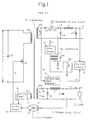
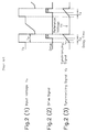
- Fig. 1 shows a conventional multi-output switching power supply provided with a primary output circuit and a secondary output circuit
- Fig. 2 shows the respective waveforms of each of the sections of Fig. 1.
- the primary output circuit 1 is an output circuit for supplying a voltage V1 which serves as the basis for a signal S1 for controlling a main switch Q1 on a primary side of a transformer T1.
- Control circuit 3 outputs a pulse width signal which renders the output voltage V1 of the primary output circuit 1 equal to a set voltage (not shown), thus controlling the duty ratio (the on rate of the switch Q1 per unit of time).
- a voltage Vw3 whose duty ratio has been changed is induced in a secondary winding W3.
- This voltage Vw3 is rectified and smoothed, and its duty ratio stabilizes at points where the primary output V1 of the circuit and the set voltage are uniform.
- Primary output circuit 1 comprises a secondary winding W3, a diode D1 for rectifying the voltage induced in the secondary winding W3, a smoothing circuit consisting of a choke coil L1 and a capacitor C1, and a diode D2 for discharging the energy stored in the choke coil L1.
- the value of the output voltage V1 of the primary output circuit 1 is isolated by a photocoupler 2, and is fed back to the primary side of the transformer T1.
- the secondary output circuit is a circuit connected to the secondary winding W2 connected to the transformer T1 but wound separately to the primary winding W3, and obtains a D.C. voltage V2 from the voltage induced in the winding W2.
- the secondary output circuit 10 is generally provided with a means for stabilizing the secondary output voltage V2.
- the stabilizing means for the secondary output circuit 10 consists of a synchronizing signal generator 6, a control circuit 5, a drive transformer T2, a drive circuit 4, and an FET Q2.
- the induction voltage Vo (refer to Fig. 2 (1)) of the winding W2 is rectified by the diode D3 and supplied to the switch element of the FET Q2.
- the on/off functions of the FET Q2 are controlled by the drive circuit 4.
- the amount of electricity passing through the FET Q2 is smoothed by the choke coil L2 and the capacitor C2, and becomes the secondary output voltage V2 which has reduced ripples.
- the diode D4 discharges the energy stored in the choke coil L2 during the off periods of the FET Q2.
- the stability of the secondary output voltage V2 is achieved by appropriately chopping, in the FET Q2, the pulse width Tp (refer to Fig. 2 (1)) of the induction voltage Vo of the winding W2, and supplying the result to the smoothing circuit (the choke coil L2 and the capacitor C2).
- the control operation of the FET Q2 will now be explained with reference to Fig. 2.
- An FET Q3 connected to the control circuit 5 carries out switching operations, while a transformer T2 carries out level changes of the output Va of the control circuit 5.
- the device shown in Fig. 1 operates in the following manner.
- a D.C. voltage Vin is generated at both ends of a capacitor C3, and the on/off functions of a switch element Q1 are controlled by a control circuit 3. Accordingly, a voltage is intermittently supplied to the primary winding W1, with the result that an induction voltage is generated in the secondary windings W2 and W3.
- the primary output voltage V1 obtained from the primary output circuit 1 is fed back to a primary side of the transformer T1 via the photocoupler 2. Then a pulse width modulation signal S1 is produced in the control circuit 3 for conforming the primary output voltage V1 to the set voltage (not shown), and the duty ratio of the switch element Q1 is controlled based thereon.
- the duty ratio of the voltage Vo induced in the secondary winding W2 fluctuates according to the input voltage Vin or the load current Iout of the primary output circuit 1. The reason for this is as follows.
- the duty ratio of the primary switch Q1 is increased. In other words, by increasing the rate at which the FET Q1 is switched on, due to the reduction of the voltage Vin, the amount of electricity supplied to winding W3 is compensated for.
- the output voltage V2 of the secondary output circuit 10 will also fluctuate. Since fluctuation of the output voltage V2 is a major problem, the device of Fig. 1 performs a control operation for rendering the secondary output voltage V2 uniform.
- the input voltage Vo supplied to the secondary output circuit 10 has a waveform as shown in Fig. 2 (1).
- the synchronizing signal generator 6 inducts the input voltage Vo, and outputs a synchronizing signal (refer to Fig.2 (3)) which increases in a "ramp" waveform ("sawtooth” waveform) only during the time period Tp when the input voltage Vo is at a high level.
- This synchronizing signal Vc is synchronized to the switching waveform of the primary side of the transformer T1; the synchronizing signal generator 6 detects the on (high) state of the induction voltage Vo of the secondary winding W2 and produces the above waveform.
- the control circuit 5 inducts both the synchronizing signal Vc having the waveform of Fig. 2 (3) and the secondary output voltage V2, and produces a reference signal VK.
- the control circuit 5 When the secondary output voltage V2 of the secondary output circuit 10 is higher than a set voltage (not shown), the above reference voltage VK (see (3) in Fig 2), produced by the control circuit 5, rises.
- the control circuit 5 outputs a high level signal Va during the period when the value of the synchronizing signal Vc shown as Fig. 2 (3) is higher than the reference voltage VK produced within the control circuit 5.
- This output signal Va of the the control circuit 5 drives the FET Q3 on/off.
- the voltage on the primary side of the drive transformer T2 is boosted and this boosted voltage is supplied to the drive circuit 4.
- the reference voltage VK shown as Fig. 2 (3)
- the period wherein the value of the synchronizing signal is higher than the reference signal VK i.e. the period when the FET Q2 is on
- the value of the secondary output voltage V2 decreases and approaches the set voltage.
- the secondary output voltage V2 when the secondary output voltage V2 is lower than the set voltage, the reference voltage decreases, and the operation described above occurs in reverse, i.e. the on period of the FET Q2 is increased, and since the amount of electricity supplied to the choke coil L2 and the capacitor C2 increases, the secondary output voltage V2 also increases, approaching the set voltage.
- MOS-FET Although generally an MOS-FET is used as the switch element Q2, if the gate potential of the MOS-FET is not at least 4 volts higher than the source potential, the MOS-FET cannot be driven on. Also, in a general junction type FET the gate potential must be higher than the source potential. Further, it is necessary to supply a signal having a voltage at least 4 volts higher than point A in Fig. 1 to the gate of the FET Q2. However, this point A is toward the high potential side of the secondary output circuit 10, so that in order to obtain a potential higher than at point A, a boosting means is necessary. In conventional devices, a drive transformer T2 is provided, to which the output Va of the control circuit is supplied, and which generates a voltage 4 volts higher than that at point A and supplies it to the gate of the FET Q2.
- the drive transformer T2 is provided between the drive circuit 4 and the control circuit 5, when the pulse width signal Va passes through the drive transformer T2, it is delayed. If we refer to this delay time as Td (see Fig. 2(3)), generally this time delay Td would be equal to about 200ns. Consequently, at a time TA the value of the synchronizing signal Vc is higher than the reference voltage VK, and takes the amount of time Td from when the control circuit 5 detects this to when the FET Q2 actually reaches the on-state (refer to Fig. 2 (2)).
- the device of Fig. 1 can only supply the amount of electricity of the maximum pulse width (Tp-Td) to the smoothing circuit via the FET Q2.
- Tp-Td the maximum pulse width
- the switching frequency of the power supply in Fig. 1 is a low frequency of around 100kHz (if the input pulse width Tp is approx. 3 microseconds)
- the delay time Td shown in Fig. 2 (3) is insignificant.
- the transformers and circuit elements are quite large. Recently, due to the miniaturization of switching power supplies, high switching frequencies are preferred in the design thereof.
- the rate of the delay time Td increases, and the delay time Td becomes significant.
- the rate of the delay time Td increases. Consequently, if a large current is to be output from the secondary output circuit, the amount of electricity supplied to the smoothing circuit (the circuit having the choke coil L2 and the capacitor C2) will be small, resulting in the problem that output cannot be maintained.
- the present invention has been made to solve the above problem, therefore a first object is to provide a switching power supply which, by reducing the delay time of a control signal Va (a signal for controlling the on/off functions of an FET Q2) by means of a drive transformer T2, can obtain a set secondary output voltage V2 which follows up and operates even under high switching frequencies.
- a control signal Va a signal for controlling the on/off functions of an FET Q2
- a second object is to provide a switching power supply which can maintain output even when the output current is large due to the reduction of the delay time of the control signal Va from the drive transformer T2.
- a third object is to provide a switching power supply which can maintain output without limiting the amount of electricity supplied to the smoothing circuit of the secondary output circuit 10 even when only a small delay of the control signal Va exists, and which can maintain output even when a large current is output.
- Fig. 1 is an block diagram of the structure of a conventional switching power supply.
- Fig. 2 is a time chart for signals of each section of the device shown in Fig. 1.
- Fig. 3 is a block diagram of an embodiment of a switching power supply of the present invention.
- Fig. 4 is a block diagram of a synchronizing signal generator used in the switching power supply of the present invention.
- Fig. 5 is a time chart for the signals of each section of the circuit shown in Fig. 4.
- Fig. 6 is a block diagram of another embodiment of the switching power supply of the present invention.
- Fig. 7 is a time chart showing the signals of each section of the device shown in Fig. 6.
- Fig. 8 is a time chart illustrating the entire operation of the device shown in Fig. 6.
- Fig. 9 is a block diagram of another embodiment of the secondary output circuit of the device shown in Fig. 6.
- Fig. 10 is a block diagram of another embodiment of the switching power supply of the present invention.
- Fig. 11 is a diagram illustrating the starting operation of the device shown in Fig. 10.
- Fig. 12 is a time chart showing the signals of each section of the device shown in Fig. 10.
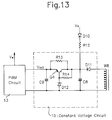
- Fig. 13 is a block diagram of a specific structure of the set voltage circuit 15 in the device shown in Fig. 10.
- Fig. 14 illustrates the mounting conditions of the switching power supply of the present invention.
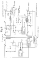
- Fig. 3 is a block diagram showing the structure of a first embodiment of the present invention.
- a main switch Q1 on a primary side of a transformer T is switched by a pulse width signal S1 supplied from a PWM circuit 23.
- This switching frequency is determined by an oscillator circuit 21.
- a pulse voltage induced in a secondary winding W3 becomes a primary output voltage V1 by the operation of a diode D1 of a primary output circuit 1 and a choke coil L1 and capacitor C1.
- This voltage V1 is then applied to a differential amplifier 24, where it is compared to a set voltage Vt to determine the value of the primary output voltage V1.
- the differential amplifier 24 which generates this type of reference signal Vk' can be easily constructed by making use of the TL431 type IC sold by Texas Instrument Co.
- a photocoupler is provided in the differential amplifier 24, and the reference signal Vk' is fed back to the PWM circuit 23 via this photocoupler.
- the PWM circuit 23 controls the duty ratio of the pulse signal S1 output on the basis of the reference voltage Vk' received as an input, the primary output voltage V1 reaches a value equal to the set voltage Vt.
- An auxiliary power supply 22 generates a D.C. voltage from the induction voltage of a winding W4 wound around the core of the transformer T, and supplies this power source voltage to the PWM circuit 23.
- diodes D3 and D4, the FET Q2, the choke coil L2, and the capacitor C2 have the same functions and effects as described in reference to Fig. 1.
- diode D3 has the function of rectifying the voltage induced in the winding W2, and the choke coil L2 and capacitor C2 constitute a smoothing circuit.
- the FET Q2 is arranged between the diode D3 and the smoothing circuit, and controls the amount of electricity entering the smoothing circuit from the winding W2 by means of an on/off operation.
- the FETs Q1 and Q2 are illustrated as elements capable of switching operations above several hundred kHz, but IGBTs (insulated gate bipolar transistors) or multipurpose transistors may also be used if they are capable of high speed switching in accordance with an on/off control signal.
- IGBTs insulated gate bipolar transistors
- multipurpose transistors may also be used if they are capable of high speed switching in accordance with an on/off control signal.
- the block 30 delineated by dotted lines in Fig. 3 is the key section for achieving the above-described objects of the present invention, and includes a synchronizing signal generator 11, an auxiliary power supply 12, a PWM control circuit 13 and a differential amplifier 14. Each of these sections is described in detail below.
- the synchronizing signal generator 11 receives as an input the signal Vsw which repeats high and low states according to the on/off states of the primary switch Q1, and outputs the sawtooth synchronizing signal Vc which repeats a fixed gradient pattern from the time when the Primary switch Q1 switches of to the time when it switches off again.
- output signal of the synchronizing signal generator of the present invention has the waveform Vc shown in Fig.5 (4), whereas the output signal of a conventional synchronizing has the waveform shown in Fig. 2 (3).
- the signal Vsw received as an input by the synchronizing signal generator 11, if it is a signal which repeats between high and low in accordance with the on/off of the main switch Q1, may be extracted from any point in the diagram of Fig. 3; for example, a signal can be received as an input from the point B at one end of the wiring W2 in Fig. 3.
- the induction voltage VB of the winding W5 wound around the choke coil L1 of the primary output circuit 1 is received as the signal Vsw.
- the induction voltage VH of the winding W8 wound around the choke coil L2 of the secondary output circuit 10 is received as the signal Vsw.
- the differential amplifier 14 receives as input the secondary output voltage V2 of the smoothing circuit (secondary output circuit 10) and set voltage Vs for setting the value of the secondary output voltage V2, and outputs the reference signal Vk.
- the differential amplifier 14 performs the same operation as the differential amplifier 24 described previously, and can employ the same structure.
- the secondary output voltage V2 is applied to the differential amplifier 14 where it is compared to a set value voltage Vs.
- the differnetial amplifier 14 then outputs a reference voltage Vk to the PWM circuit 13.
- the value of the reference signal Vk if the secondary output signal V2 is greater than the set voltage Vs, increases, and conversely, if V2 is less than Vs, decreases. If Vs equals V2, the value VK stabilizes by a given voltage level. Since this differential amplifier 14 has the same structure as the differential amplifier 24 described above, it can easily be constructed using a TL431 type special use IC which is widely sold.
- the auxiliary power supply 12 generates a D.C. voltage Vcc which has a voltage level higher than the potential at the source (point A) of the FET Q2 and is able to drive the FET Q2 on.
- This auxiliary power supply can have any type of structure as long as it can output a D.C. current Vcc of the above voltage level, but in this case the structure illustrated in Figs. 6 and 10 is preferable.
- the auxiliary power supply receives the potential as inputat point A.
- a line is provided connecting the point D of the first winding W1, which acts as a starter circuit, to the auxiliary power supply 22, and serves to supply a voltage when the auxiliary power supply starts.
- the PWM circuit 13 makes the D.C. voltage Vcc, obtained from the auxiliary power source 12, a power source voltage, and receives the synchronizing signal Vc as input from the synchronizing signal generator 11 and the reference signal Vk from the differential amplifier. The PWM circuit then compares which of the 2 signals Vc and Vk received as input is high and low and applies the resultant signal Ve directly to the gate of the FET Q2, driving it on or off.
- Vc when comparing the 2 signals Vc and Vk, if Vc > Vk, the PWM circuit sets the output Ve high, and if Vc ⁇ Vk, sets the output Ve low.
- This type of function can easily be realized by using a commonly sold comparator
- the first feature of the device shown in Fig.3 is that a drive transformer (refer to T2 in Fog.1) is not used to obtain the signal for driving the FET Q2, but rather a D.C. voltage Vcc is produced in the auxiliary power supply 12, and the control signal Ve of the FET Q2 is generated in the PWM circuit which utilizes the above D.C. voltage Vcc as a power supply.
- a drive transformer (refer to T2 in Fog.1) is not used to obtain the signal for driving the FET Q2, but rather a D.C. voltage Vcc is produced in the auxiliary power supply 12, and the control signal Ve of the FET Q2 is generated in the PWM circuit which utilizes the above D.C. voltage Vcc as a power supply.
- the second feature as shown as (4) in Fig.5, is that the waveform of the synchronizing signal Vc, between each time when the primary switch turns off and the next time it turns off, is a repeating fixed gradient waveform.
- the auxiliary power supply 12 because it receives the potential as input from point A shown in Fig. 3, can supply a voltage Vcc higher than at point A as a power supply to the PWM circuit. Consequently, since the PWM circuit can apply a voltage approximately Vcc higher than at point A to the gate of the FET Q2, it can drive the FET Q2 directly without going through a drive transformer (T2in Fig. 1).
- the power source for the auxiliary power supply can be taken from the choke coil L1 as shown in Fig. 6, or from the choke coil L2 as shown in Fig. 10.
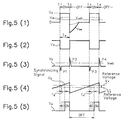
- Fig. 4 shows the concrete structure of the synchronizing signal generator 11, while Fig. 5 shows the signal waveforms of each section shown in Fig. 5.
- the signal Vsw in Fig. 4 will be explained as introduced from point B in Fig. 3.
- a comparator U1 having diodes D5 and D6, resistors R1 to R4 and a reference voltage Vref1, and a capacitor C4 constitute an off-timing detector for detecting the off-timing of the primary switch Q1.
- a comparator U2 having a reference voltage Vref2, a diode D7, resistors R5 and R6, and a capacitor C5 consistute a waveform generator.
- Winding W2 generates a switching waveform shown as (1) in Fig. 5.
- t1 to t2 and t3 to t4 are periods at which the primary switch Q1 is on, and t2 to t3 is the period at which the primary switch Q1 is off.
- this waveform Va is a square waveform whose polarity reverses at the edges t1, t2, t3, etc. of the waveform of Fig. 5 (1) (the waveform of the winding W2).
- a differential waveform Vb as shown in Fig. 5 (3),synchronized with the edges of the output voltage Vo of the winding W2 (see Fig. 5 (1)), is applied to the input terminal (-) of the comparator U2.
- the pulses P2 and P4 of the differential waveform Vb are generated and synchronized with the off timing of the primary switch Q1.
- the comparator U2 receivesas input differentail pulses P1, P2, P3, etc. shown in Fig. 5 (3) at the input terminal (-), and the reference voltage Vref2 at the input terminal (+)and compares them.
- the refernce voltage Vref2 is less than the high value of differential pulses P2 and P4, therefore the output of the comparator U2 rapidly changes to a minus potential. Accordingly,in the circuit of the capacitor C5 and the diode D7, a current i1 flows as shown in Fig. 4, and the charge stored in the capacitor C5 discharges.
- the comparator U2 when the differential pulse P2 disappears, the potential of the input terminal (+) becomes higher than the potential of the input terminal (-), therefore the output thereof reaches an even higher level. Consequently, the diode D7 is off, and the potential of capacitor C5 rises in a uniform gradient to the potential divided by resistors R5 and R6 connected between the common potential of the capacitor C5 and the power supply Vcc. In other words, the signal Vc which is the voltage of the capacitor C5 is becomes a "ramp" waveform which rises in a fixed gradient (see Fig. 5 (4)).
- the maximum voltage and gradient of the synchronizing signal Vc of Fig. 5 (4) is determined by the values of the resistors R5 and R6, and the capacity of the capacitor C5.
- the secondary output circuit of the device shown in Fig. 3 operates in the following manner. As described previously, a switching waveform as shown in Fig. 5 (1)is generated in the winding W2,and the sawtooth synchronizing signal Vc having the shown in Fig. 5 (4) is output from the synchronizing signal generator 11.
- the PWM circuit 13 compares the reference voltage Vk, which changes as described above, and the synchronizing Vc(see Fig. 5 (4)), and when the reference voltage Vk is less than the value of the synchronizing signal, a control signal Ve having the waveform shown in Fig. 5 (5) is applied to the gate of the FET Q2.
- the FET Q2 reaches an on state when the signal Ve is high.
- the PWM circuit 13 receives from the auxiliary power supply 12 the voltage Vcc which is large enough to drive the FET Q2 on. Consequently, the signal Ve output from the PWM circuit 13 has a voltage level which can turn on the FET Q2.
- This type of device shown in Fig. 3 can produce the control signal Ve shown in Fig. 5 (5) without using the drive transformer T2 shown in Fig. 1. Accordingly, the delay time of the control signal Ve of the device shown in Fig. 3 can be greatly reduced over the delay time of the control signal Ve in the conventional device shown in Fig. 1.
- the device of Fig. 3 can allow the switching operation of the FET Q2 to follow this frequency. In short, it can achieve the first and second objects of the present invention.
- the delay time of the device of Fig. 3 has a greatly reduced value, in order to decrease the effect of the delay time, in the present invention the synchronizing signal Vc has a waveform of a repeating fixed gradient from the time when the primary switch Q1 switches to off to the next time it switches off. Therefore, the entire input pulse width Tp, i.e. the total amount of electricity input from the winding W2 to the seocndary output circuit 10, can be accurately passed to the smoothing circuit, and the third object of the present invention can be achieved.
- the on state of the FET Q2 is the time period when the refence voltage Vk is less than the value of the synchronizing signal Vc (see Fig. 5 (4)). Since the waveform of the synchronizing signal Vc of the present invention is a repeating fixed gradient waveform which occurs from the time when the primary switch Q1 reaches an on state to the time it reaches the next on state, if the level of the refernce voltage drops, the on period of the FET Q2 can be increased. In other words, because the voltage level of the reference voltage Vk drops until the output voltageV2 of the secondary output circuit equals the set voltage Vs (see Vk' of Fig. 5 (4)), the pulse width of the signal Ve can be widened (see Fig.
- FIG. 6 is a block diagram of the second embodiment of the present invention showing a concrete example of the auxiliary power supply 12 in Fig. 3.
- the points where the device of Fig. 6 differs from the device of Fig. 3 are:
- winding W6 which constitutes the auxiliary power supply 12 is wound around the core of the choke coil L1 constituting the primary output circuit 1, and one end thereof is connected to point A at the source side of the FET Q2.
- Winding W5 which forms the choke coil L1 and the newly wound winding W6 are wound in a flyback connecting relationship as shown in Fig. 6 (refer to the two dots of the choke coil L1 section).
- Synchronizing signal generator 11 receives as input the induction voltage VB of the winding W6, and outputs the sawtooth synchronizing waveform Vc which repeats at a constant gradient from when the primary switch Q1 turns off to when it turns off again next.
- the structure and operation of the synchronizing signal generator 11 have already been described with refernce to Fig. 4.
- the auxiliary power supply 12 obtains a D.C. voltage Vcc which is the result of rectifying and smoothing the square waveform voltage VB induced in the winding W6 with the diode D8 and the capacitor C7.
- the D.C. voltage Vcc obtained by simply rectifying and smoothing is a stabilized voltage. The reason for this is as follows.
- Primary output circuit 1 is controlled to a set voltage V1 by the PWM circuit 23 on one side of the transformer T. Accordingly, since the energy Va*Tp stored in the winding W5 of the choke coil L1 becomes fixed , the energy Vb*(Td-Tp) induced in the winding W6 is fixed.
- the D.C. voltage Vcc obtained simply by rectifying and smoothing the voltage VB by means of the diode D8 and the capacitor C7, is a stabilized voltage.
- This obtained D.C. voltage Vcc is Vcc volts higher than the voltage at point A.
- the first feature of the device shown in Fig. 6 resides in that another winding W6 is provided for the choke coil L1 of the primary circuit 1, and a D.C. voltage Vcc higher than point A is obtained from this winding W6.
- the second feature is that the basic timing signal for producing the synchronizing signal Vc, is produced from the induction voltage VB of the winding W6 wound round the choke coil L1 of the primary output circuit 1.
- the waveform of the voltage VA as shown in Fig. 7 (1) is induced in the winding W5 of the choke coil L1.
- Times t1 to t2 and t3 to t4 are the periods when the primary switch Q1 is on, and the time t2 to t3 is the period when the primary switch is off.
- Windings W5 and W6 have a flyback connecting relationship, and if the induction voltage VB of the winding W6 (see Fig. 7 (2)) is rectified and smoothed, the primary voltage V1 will be stabilized, therefore a stable floating voltage Vcc (of e.g. 15V) is obtained from the auxiliary power supply 12.
- the auxiliary power supply 12 since they are in a flyback relationship, during the time when the choke coil L1 is off in relation to the primary output circuit, the auxiliary power supply 12 operates so as to receive electricity (see Fig. 7 (2)) as input. Even if the auxiliary power supply 12 is connected, there is no effect on the stability of the primary output voltage V1.
- the auxiliary power supply 12 can supply to the PWM circuit 13 a voltage Vcc higher than that at point A as a power source voltage. Because the PWM circuit 13 makes the voltage Vcc a power source voltage, a control signal Ve of a voltage about Vcc volts higher than point A can be applied to the gate of the FET Q2. Thus, the on/off drive of the FET Q2 can be performed without a drive transformer (see Fig. 1).
- the pulse waveform VB shown in Fig. 7 (2) is applied to the synchronizing signal generator.
- This pulse waveform VB represents the on/off operation of the primary switch Q1, therefore the synchronizing signal generator 11, as already explained above in Fig. 4, with the knowledge of the leading edges of the waveform VB, can grasp the state from the point where the primary switch goes off till the next point where it goes off.
- a "sawtooth" waveform Vc which repeats a fixed gradient pattern as shown in Fig. 7 (3) is output.
- PWM circuit 13 compares a reference voltage Vk which changes as described above and the synchronizing signal Vc, and the result thereof, as shown in Fig. 7 (4), is a pulse width control signal Ve which is applied to the FET Q2 and drives the on/off thereof.
- the timing signal which is the origin from which the synchronizing signal is produced (the signal which is the on/off signal of the primary switch Q1) is not received as input from the winding W2 of the transformer T, but is instead introduced from the choke coil L1 of the primary output circuit 1, this device has the advantage that the electrical components constituting the synchronizing signal generator 11 need not be high tolerance components.
- the initial operation of the device of Fig. 6 is as follows. Firstly, immediately after the D.C. voltage Vin is applied, the FET Q1 is not performing on/off switching. consequently, the transformer T does not generate an inductance voltage, therefore the auxiliary power supply 22 cannot supply a voltage to the PWM circuit 23.
- the voltage at point D in Fig. 6 (the voltage at the terminal of the capacitor C3) is introduced into the auxiliary power supply 22. Accordingly, the auxiliary power supply 22, at the starting time, produces a given voltage level with the voltage of point D, and supplies it to the PWM circuit. By this means the PWM circuit 23 begins operation. When the PWM circuit 23 begins operation, and the winding W4 generates an actual induction voltage, the auxiliary power supply 22 no longer requires the voltage from point D. Then, the D.C. current to be supplied to the PWM circuit 23 is produced by an inductance voltage from the winding W4.
- Stoppage of the operation of the device shown in Fig. 6 is as follows. If the operation of the PWM circuit 23 stops, the primary output voltage V1 drops, hence the secondary output voltage Vcc of the auxiliary power supply 12 also drops. When voltage Vcc reaches the operation limit VM' of the PWM circuit 13, the PWM circuit 13 ceases that operation (refer to Fig. 8 (3)).
- the operations of the primary output circuit 1 and the secondary output circuit 10 can be driven in cooperation. Also, there is the advantage that by looking at the voltage VA of the choke coil of the primary output circuit, the input voltage Vin can be observed.
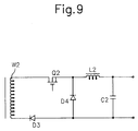
- Fig. 9 shows a different design of the choke coil L2, the capacitor C2, the diode D3 and the FET Q2 of the secondary output circuit 10 of the device shown in Fig. 6.
- the above explanation is of a so-called primary side control method with the PWM circuit 23 arranged on a primary side of the transformer T, but the present invention can be realized with a so-called secondary side method with the PWM circuit 23 arranged on a second side of the transformer T.
- the output S1 of the PWM circuit 23 may for example be isolated by a tranformer (not shown) and supplied to the primary switch Q1
- Fig. 10 is a block diagram showing the structure of the third embodiment of the present invention, and specifically shows the auxiliary power source in Fig. 3.
- the points in which Fig. 10 differs from Fig. 3 are as follows.
- the winding W8 constituting the auxiliary power supply 12 is wound around the core of the choke coil L2 provided in the secondary output circuit 10. One end of this winding W8 is connected to a point A at the source side os the FET Q2.
- the auxiliary power supply 12 obtains a D.C. voltage Vcc2 by regulating the induction voltage VH from the winding W8 of the choke coil L2. Since the induction voltage of the winding W8 can be decided by the number of turns in the winding W8, the D.C. voltage Vcc2 can be appropriately determined by the nuber of turns in the winding W8, so that a voltage which is sufficient to drive the FET Q2 can be produced.
- the auxiliary power supply 12 of Fig. 10 obtain its power from the choke coil L2 of the secondary voltage circuit 10.
- the winding W8 is wound around the core of the choke coil L2 constituting the secondary output circuit 10, and one end thereof is connected to point A at the source side of the FET Q2.
- the synchronizing signal generator 11 receives as input the induction voltage VH of the winding W8, and outputs a sawtooth synchronizing waveform Vc which repeats a fixed gradient pattern between the time when the primary switch Q1 turns off and the next time when it turns off.
- the structure and operation of the synchronizing signal have already been explained with reference to Fig. 4.
- the auxiliary power source 12 of Fig. 10 differs from the auxiliary power supply of Fig. 6 in that it provides a diode D10 and a resistor R12 which constitute a starter circuit.
- the reason for providing a starter circuit is as follows. In the device of Fig. 10, when operation begins, the FET Q2 is still off, therefore a voltage is not generated in the choke coil of the secondary power supply 10. Consequently, a voltage VH is not generated in the winding W8, hence the fixed voltage circuit 15 cannot produce the voltage Vcc2 which is to be supplied to the PWM circuit 13.
- the voltage Vo is received as input from the winding W2 of the transdormer T via the diodde D10 and the resistor R12 to the auxiliary power supply, and from there a voltage Vcc2 of a given level is produced.
- the FET Q2 begins its on/off operation.
- a voltage VH is induced in the winding W8 of the choke coil L2 of the secondary output circuit 10.
- the auxiliary power supply 12 produces not the voltage supplied from the diode D10 and the resistor R12, but produces a voltage Vcc2 with the induction voltage VH of the winding W8, whereby starting is completed.
- Fig. 13 is a diagram of a concrete example of auxiliary power source 12 having a starter circuit as described above.
- the diode D10, the resistor R12, the winding W8, the set voltage circuit 15 and the PWM circuit 13 are all the same as in afig. 10.
- the set voltage circuit 15 comprises a diode D11, capacitors C8 and C9, a transistor Q4, a Zenner diode D12 and a resistor R14.
- the induction voltage Vo (refer to Fig. 10) of the winding W2 is rectified by the diode D10 and applied to the set voltage circuit 15.
- This rectified current flows along the channel from resistor R12 to resistor R23 to capacitor C9, and charges the capacitor C9.
- the voltage Vcc2 of the capacitor C9 by means of the current from the starter circuit, gradually rises, and can put the PWM circuit into operating condition.
- the FET Q2 of Fig. 10 performs the on/off operation, and an induction voltage is produced in the wiring W8. Consequently, the voltage of the capacitor C8 increases, and the transistor Q4 produces a set voltage Vcc2 with the electricity from the winding W8. Also, when the potential of the capacitor C8 increases, the diode D10 of the starter circuit reaches a reverse bias state and cuts off.
- the first feature of the device shown in Fig. 10 is that a new winding W8 is provided in the choke coil L2 of the secondary output circuit 10, and that from this winding W8 a D.C. voltage Vcc2, higher than the voltage at point A, is produced.
- the second feature is that a timing signal which is the basis from which the synchronizing signal Vc is produced is generated from the induction voltage VH of the winding W8 wound round the choke coil L2 of the secondary output circuit 10.
- the waveform of a voltage VH as shown in Fig. 12 (1) is induced in the winding W8 of the choke coil L2.
- the times t1 to t2 and t3 to t4 are the on periods of the primary switch Q1
- the period t2 to t3 is the off period of the primary switch Q1.
- the auxiliary power source 12 can supply to the PWM circuit 13 a power source voltage Vcc2 volts higher than at point A. Accordingly, since the PWM circuit 13 can apply a control signal Ve of a voltage approximately Vcc2 volts higher tha that at point A to the gate of the FET Q2, the FET Q2 can be driven without the use of a drive transformer T2 (see Fig. 1).
- the pulse waveform VH shown in Fig. 12 is supplied to the synchronizing signal generator 11.
- This pulse waveform VH describes the on/off of the primary switch Q1, hence the synchronizing signal generator 11 recognizes the trailing edge of the waveform VH, and can hold from when the primary switch goes off till the next time the primary switch goes off.
- the synchronizing signal generator 11 outputs a synchronizing signal Vc which, in the time period shown in Fig. 12 (2), repeats a fixed gradient pattern.
- the PWM circuit 13 carries out a large/small comparison of the changing reference voltage Vk and the synchronizing signal Vc, and supplies a control signal Ve, which is the result of the above operation and which controls the pulse width as shown in Fig. 12 (3), to the FET Q2, thus driving the FET Q2 on and off.
- the timing signal which is the basis on which the synchronizing signal is produced (the on/off signal of the primary switch Q1) is taken from the transformer T and received as an input from the choke coil L2 of the secondary output circuit 10, hence the electrical components which constitute the the synchronizing signal generator 11 need not be high-tolerance components.
- auxiliary power supply 22 has the same structure and operation as the auxiliary power source 12 described above with reference to Fig. 13, and raises the output voltage Vcc1 as shown in Fig. 11 (2) by means of the voltage supplied via the resistor R11.
- the voltage Vo supplied to the auxiliary power supply 12 from the primary transformer T corresponds, in the auxiliary power supply 22, to the voltage Vin supplied via the resistor R11. Since the voltage Vin is a direct current, there is no necessity for a diode to be provided in the line connecting the capacitor C3 and the auxiliary power supply 22 and including the resistor R11. Also, the voltage VH of the winding W8 of the choke coil L2 supplied to the auxiliary power supply 12 corresponds, in the auxiliary power supply 22, to the voltage from the winding W4 wound round the primary transformer T.
- the oscillation circuit and the PWM circuit function,hence the primary switch Q1 begins its on/off operation. Accordingly, since the primary output circuit 1 begins to operate, the primary output voltage V1 ascends as shown in Fig. 11 (3).
- the differential amplifier 24 receives as an input the primary output voltage V1 and the set voltage Vt and, as described previously, feeds back a reference signal Vk' to the PWM circuit 23.
- the PWM circuit 23 performs the aforementioned operation; the primary output voltage V1 stabilizes when it becomes the same as the set voltage Vt.
- the auxiliary power supply 22 When the primary voltage V1 rises, power is supplied to the auxiliary power supply 22 from the winding W4, the auxiliary power supply changes to a D.C. voltage Vin, and generates an output voltage Vcc1 from the power supplied from the winding W4. At this time, the power inflow from the D.C. voltage Vin to the auxiliary power supply is intercepted.
- the induction voltage Vo of the secondary winding W2 of the primary transformer T also rises as shown in Fig.11 (4).
- This induction voltage Vo is supplied to the auxiliary power source 12 of the secondary output circuit 10 via the diode D10 and the resistor R12.
- the output voltage Vcc2 of the increases as shown in Fig. 11 (5). If the value of the output voltage Vcc2 of the auxiliary power supply 12 increases beyond the start voltage Vth2 of the PWM circuit 13, the PWM circuit 13 begins to function, and switches the FET Q2. Accordingly, the pulse power of the induction voltage Vo of the winding W2 is supplied to the smoothing circuit via the FET Q2, and the secondary output circuit 10 rises. In short, the secondary output voltage increases as shown in Fig. 11 (6).
- the seondary output voltage V2 is compared to the set voltage Vs by the differential amplifier 14, the resultant reference voltage Vk is fed back to the PWM circuit 13, and the secondary output voltage V2 is stabilized.
- the circuits constituting each of the primary circuit 1 and the secondary circuit 10 can employ the same types of components. Also , the FET Q2 can be driven directly by the output of the PWM circuit without the necessity for insulation.
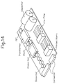
- Fig. 14 is a perspective diagram of the structure of the switching power supply.
- the print board is made from an aluminum-type high electrical and high heat conductive material, the upper surface thereof radiating heat originating from the mounted electrical components; essentially the entire lower of the print board serves as a heat sink.
- the transformers, line filters, choke coils, and other magnetic components are mounted, as well as electrical and smoothing capacitors.
- diodes, FETs and other switching components from which radiation originates are mounted on the upper surface; apart from these, other components such as resistors are also mounted on the same side of the print board.
- These diodes, FETs, resistors and other devices are surface mounted-devices (SMD) for mounting easily these devices on the print board.
- SMD surface mounted-devices
- the production automation and design automation of power supplies can be considerably advanced.
- the invention utilizes miniaturized components mounted on the upper surface of a one-sided print board, therefore guidance of conveyor robots is easily accomplished, and production mechanization is advanced.
- radiation design the temperature distribution of the print board lower surface was tested with a computer simulation model, if only the conditions of a casing for receiving the power supply are given,it is possible to determine whether or not the rise in the temperature of the power supply is within an allowable range.
- EMI countermeasures since thew floating capacity can be measured beforehand, the radiated electromagnetic waves can be forecast accurately by a computer simulation, and determining countermeasures can be easily done by carrying out a practical test.
- vibration countermeasures the heavy magnetic components are in direct contact with the upper surface of the pr board, therefore the center of gravity is low and earthquake resistance is improved. In this manner, there is the advantage of ease of designing in view of radiation design, EMI countermeasures, and vibration countermeasures.
Applications Claiming Priority (2)
| Application Number | Priority Date | Filing Date | Title |
|---|---|---|---|
| JP5000276A JPH06209569A (ja) | 1993-01-05 | 1993-01-05 | スイッチング電源装置 |
| JP276/93 | 1993-01-05 |
Publications (3)
| Publication Number | Publication Date |
|---|---|
| EP0605752A2 EP0605752A2 (en) | 1994-07-13 |
| EP0605752A3 EP0605752A3 (en) | 1996-03-13 |
| EP0605752B1 true EP0605752B1 (en) | 1998-07-22 |
Family
ID=11469386
Family Applications (1)
| Application Number | Title | Priority Date | Filing Date |
|---|---|---|---|
| EP93104489A Expired - Lifetime EP0605752B1 (en) | 1993-01-05 | 1993-03-18 | Switching power supply |
Country Status (6)
| Country | Link |
|---|---|
| US (1) | US5424932A (ja) |
| EP (1) | EP0605752B1 (ja) |
| JP (1) | JPH06209569A (ja) |
| CN (1) | CN1041039C (ja) |
| CA (1) | CA2094971C (ja) |
| DE (1) | DE605752T1 (ja) |
Families Citing this family (104)
| Publication number | Priority date | Publication date | Assignee | Title |
|---|---|---|---|---|
| US5559423A (en) * | 1994-03-31 | 1996-09-24 | Norhtern Telecom Limited | Voltage regulator including a linear transconductance amplifier |
| AT404306B (de) * | 1994-08-22 | 1998-10-27 | Siemens Ag Oesterreich | Sperrwandlerschaltung |
| US5559683A (en) * | 1994-09-30 | 1996-09-24 | Apple Computer, Inc. | Flyback switching power supply with bootstrapped gate drive |
| KR100241401B1 (ko) * | 1995-02-14 | 2000-02-01 | 전주범 | 보조 전원 공급회로 |
| US5903140A (en) * | 1995-07-26 | 1999-05-11 | Bensys, Inc. | Low dissipation controllable electron valve |
| ATE173569T1 (de) * | 1995-07-31 | 1998-12-15 | Hewlett Packard Co | Sperrwandler |
| US5742491A (en) * | 1995-08-09 | 1998-04-21 | Lucent Technologies Inc. | Power converter adaptively driven |
| US5841313A (en) * | 1995-08-30 | 1998-11-24 | Cherry Semiconductor Corporation | Switch with programmable delay |
| US5638262A (en) * | 1995-09-07 | 1997-06-10 | Dell Usa L.P. | Method and apparatus for providing isolated power sourced from bleeder current |
| DE19540512A1 (de) * | 1995-10-31 | 1997-05-15 | Kommunikations Elektronik | Schaltungsanordnung zur Erzeugung von betragsmäßig unterschiedlichen Gleichspannungen |
| DE59708621D1 (de) * | 1996-12-17 | 2002-12-05 | Papst Motoren Gmbh & Co Kg | Schaltnetzteil |
| US7269034B2 (en) | 1997-01-24 | 2007-09-11 | Synqor, Inc. | High efficiency power converter |
| DE19711817A1 (de) * | 1997-03-21 | 1998-09-24 | Abb Daimler Benz Transp | Schaltnetzteil |
| US6055170A (en) * | 1997-06-02 | 2000-04-25 | Srmos, Inc. | Prediction methods and circuits for operating a transistor as a rectifier |
| ES2143406B1 (es) * | 1998-03-30 | 2000-12-16 | Cit Alcatel | Convertidor conmutado con multiples salidas reguladoras. |
| US6069800A (en) * | 1998-07-31 | 2000-05-30 | Astec International Limited | Line harmonic correcting flyback power converter |
| US6342737B1 (en) * | 1998-11-10 | 2002-01-29 | Lester R. Brodeur | Binary demand feedback DC/DC converter |
| US6222747B1 (en) * | 1999-01-12 | 2001-04-24 | Artesyn Technologies | Post regulation control circuit for a switch mode power supply with multiple outputs |
| DE29901322U1 (de) * | 1999-01-28 | 1999-07-08 | Melcher Ag | Spannungskonverter |
| JP2000305641A (ja) * | 1999-04-20 | 2000-11-02 | Canon Inc | スイッチング電源回路 |
| US6195271B1 (en) * | 1999-04-21 | 2001-02-27 | International Business Machines Corporation | AC adaptor with power consumption reduction in unused state |
| US6191959B1 (en) * | 1999-05-14 | 2001-02-20 | U.S. Philips Corporation | Switched-mode power supply with capacitor controlled power supply |
| DE60112244T2 (de) * | 2000-01-28 | 2006-02-09 | Ericsson Inc., Plano | Vereinfachte implementierung der parallelschaltung von synchrongleichrichter-modulen |
| WO2001082460A1 (fr) * | 2000-04-21 | 2001-11-01 | Fujitsu Limited | Convertisseur continu-continu de commutation |
| US6233165B1 (en) * | 2000-05-15 | 2001-05-15 | Asic Advantage, Inc. | Power converter having a low voltage regulator powered from a high voltage source |
| DE10059644A1 (de) * | 2000-12-01 | 2002-06-13 | Siemens Ag | Schaltungsanordnung für DC/DC-Wandler mit niedriger Ausgangsspannung |
| JP2003319649A (ja) * | 2002-02-22 | 2003-11-07 | Ricoh Co Ltd | 画像形成装置の電源回路および画像形成装置の電源制御方法 |
| JP3712064B2 (ja) * | 2002-05-08 | 2005-11-02 | セイコーエプソン株式会社 | 出力過電流保護回路、及び該出力過電流保護回路を備えた定電圧スイッチング電源回路 |
| ITTO20020545A1 (it) * | 2002-06-21 | 2003-12-22 | St Microelectronics Srl | Circuito di controllo in modalita' pwm per la post-regolazione di alimentatori a commutazione a molte uscite |
| KR100470593B1 (ko) * | 2002-09-18 | 2005-03-10 | 삼성전자주식회사 | 키오프기능을 갖는 전자기기의 전원 제어장치 |
| US20040125621A1 (en) * | 2002-12-30 | 2004-07-01 | Ta-Yung Yang | Synchronous rectifier of flyback power converter |
| DE10330605A1 (de) * | 2003-07-07 | 2005-01-27 | Deutsche Thomson-Brandt Gmbh | Schaltnetzteil |
| DE10334338A1 (de) * | 2003-07-28 | 2005-03-03 | Friwo Mobile Power Gmbh | Gesteuerter Synchrongleichrichter zum Regeln einer Ausgangsspannung eines Schaltnetzteils |
| JP3795499B2 (ja) * | 2003-12-26 | 2006-07-12 | 富士重工業株式会社 | 蓄電素子の電圧均等化装置 |
| ITMI20040383A1 (it) * | 2004-03-02 | 2004-06-02 | St Microelectronics Srl | Circuito per ridurre le varizioni della tensione di autoalimetazione di un circuito di controllo di un alimentatore a commutazione |
| JP4671019B2 (ja) * | 2005-01-14 | 2011-04-13 | サンケン電気株式会社 | 多出力型dc−dcコンバータ |
| CN100394343C (zh) * | 2005-05-24 | 2008-06-11 | 重庆宇通仪器仪表有限公司 | 参数式开关稳压电源及其控制电路 |
| US7515442B2 (en) * | 2005-05-27 | 2009-04-07 | Semiconductor Components Industries, L.L.C. | Secondary side controller and method therefor |
| US7723864B2 (en) * | 2005-07-26 | 2010-05-25 | Norgren, Inc. | AC-to-DC electrical switching circuit |
| JP4826795B2 (ja) * | 2007-02-20 | 2011-11-30 | Tdkラムダ株式会社 | 同期回路 |
| US7804256B2 (en) | 2007-03-12 | 2010-09-28 | Cirrus Logic, Inc. | Power control system for current regulated light sources |
| US8018171B1 (en) | 2007-03-12 | 2011-09-13 | Cirrus Logic, Inc. | Multi-function duty cycle modifier |
| US8076920B1 (en) | 2007-03-12 | 2011-12-13 | Cirrus Logic, Inc. | Switching power converter and control system |
| US8723438B2 (en) * | 2007-03-12 | 2014-05-13 | Cirrus Logic, Inc. | Switch power converter control with spread spectrum based electromagnetic interference reduction |
| US7667408B2 (en) * | 2007-03-12 | 2010-02-23 | Cirrus Logic, Inc. | Lighting system with lighting dimmer output mapping |
| JP2008236551A (ja) * | 2007-03-22 | 2008-10-02 | Nec Corp | 光伝送用トランシーバ及びその送信方法 |
| US7554473B2 (en) * | 2007-05-02 | 2009-06-30 | Cirrus Logic, Inc. | Control system using a nonlinear delta-sigma modulator with nonlinear process modeling |
| US8102127B2 (en) | 2007-06-24 | 2012-01-24 | Cirrus Logic, Inc. | Hybrid gas discharge lamp-LED lighting system |
| JP4995277B2 (ja) * | 2007-06-28 | 2012-08-08 | 新電元工業株式会社 | 双方向dc/dcコンバータ |
| US8008898B2 (en) * | 2008-01-30 | 2011-08-30 | Cirrus Logic, Inc. | Switching regulator with boosted auxiliary winding supply |
| US8022683B2 (en) * | 2008-01-30 | 2011-09-20 | Cirrus Logic, Inc. | Powering a power supply integrated circuit with sense current |
| US8576589B2 (en) | 2008-01-30 | 2013-11-05 | Cirrus Logic, Inc. | Switch state controller with a sense current generated operating voltage |
| US8008902B2 (en) * | 2008-06-25 | 2011-08-30 | Cirrus Logic, Inc. | Hysteretic buck converter having dynamic thresholds |
| US8847719B2 (en) * | 2008-07-25 | 2014-09-30 | Cirrus Logic, Inc. | Transformer with split primary winding |
| US8344707B2 (en) | 2008-07-25 | 2013-01-01 | Cirrus Logic, Inc. | Current sensing in a switching power converter |
| US8212491B2 (en) * | 2008-07-25 | 2012-07-03 | Cirrus Logic, Inc. | Switching power converter control with triac-based leading edge dimmer compatibility |
| US8487546B2 (en) * | 2008-08-29 | 2013-07-16 | Cirrus Logic, Inc. | LED lighting system with accurate current control |
| US8179110B2 (en) | 2008-09-30 | 2012-05-15 | Cirrus Logic Inc. | Adjustable constant current source with continuous conduction mode (“CCM”) and discontinuous conduction mode (“DCM”) operation |
| US8222872B1 (en) | 2008-09-30 | 2012-07-17 | Cirrus Logic, Inc. | Switching power converter with selectable mode auxiliary power supply |
| US8288954B2 (en) * | 2008-12-07 | 2012-10-16 | Cirrus Logic, Inc. | Primary-side based control of secondary-side current for a transformer |
| US8362707B2 (en) * | 2008-12-12 | 2013-01-29 | Cirrus Logic, Inc. | Light emitting diode based lighting system with time division ambient light feedback response |
| US8299722B2 (en) | 2008-12-12 | 2012-10-30 | Cirrus Logic, Inc. | Time division light output sensing and brightness adjustment for different spectra of light emitting diodes |
| US7994863B2 (en) * | 2008-12-31 | 2011-08-09 | Cirrus Logic, Inc. | Electronic system having common mode voltage range enhancement |
| US8482223B2 (en) * | 2009-04-30 | 2013-07-09 | Cirrus Logic, Inc. | Calibration of lamps |
| US8248145B2 (en) * | 2009-06-30 | 2012-08-21 | Cirrus Logic, Inc. | Cascode configured switching using at least one low breakdown voltage internal, integrated circuit switch to control at least one high breakdown voltage external switch |
| US8212493B2 (en) * | 2009-06-30 | 2012-07-03 | Cirrus Logic, Inc. | Low energy transfer mode for auxiliary power supply operation in a cascaded switching power converter |
| US8963535B1 (en) | 2009-06-30 | 2015-02-24 | Cirrus Logic, Inc. | Switch controlled current sensing using a hall effect sensor |
| US8198874B2 (en) * | 2009-06-30 | 2012-06-12 | Cirrus Logic, Inc. | Switching power converter with current sensing transformer auxiliary power supply |
| US9155174B2 (en) * | 2009-09-30 | 2015-10-06 | Cirrus Logic, Inc. | Phase control dimming compatible lighting systems |
| US9178415B1 (en) | 2009-10-15 | 2015-11-03 | Cirrus Logic, Inc. | Inductor over-current protection using a volt-second value representing an input voltage to a switching power converter |
| US8487591B1 (en) | 2009-12-31 | 2013-07-16 | Cirrus Logic, Inc. | Power control system with power drop out immunity and uncompromised startup time |
| US8654483B2 (en) | 2009-11-09 | 2014-02-18 | Cirrus Logic, Inc. | Power system having voltage-based monitoring for over current protection |
| US20110278938A1 (en) * | 2010-05-12 | 2011-11-17 | Magistor Technologies, L.L.C. | Ac battery employing magistor technology |
| US8569972B2 (en) | 2010-08-17 | 2013-10-29 | Cirrus Logic, Inc. | Dimmer output emulation |
| US8912781B2 (en) | 2010-07-30 | 2014-12-16 | Cirrus Logic, Inc. | Integrated circuit switching power supply controller with selectable buck mode operation |
| US8536799B1 (en) | 2010-07-30 | 2013-09-17 | Cirrus Logic, Inc. | Dimmer detection |
| US8866452B1 (en) | 2010-08-11 | 2014-10-21 | Cirrus Logic, Inc. | Variable minimum input voltage based switching in an electronic power control system |
| US9510401B1 (en) | 2010-08-24 | 2016-11-29 | Cirrus Logic, Inc. | Reduced standby power in an electronic power control system |
| US9351356B2 (en) | 2011-06-03 | 2016-05-24 | Koninklijke Philips N.V. | Primary-side control of a switching power converter with feed forward delay compensation |
| EP2715924A1 (en) | 2011-06-03 | 2014-04-09 | Cirrus Logic, Inc. | Control data determination from primary-side sensing of a secondary-side voltage in a switching power converter |
| WO2013090777A2 (en) | 2011-12-14 | 2013-06-20 | Cirrus Logic, Inc. | Isolation of secondary transformer winding current during auxiliary power supply generation |
| US9520794B2 (en) | 2012-07-25 | 2016-12-13 | Philips Lighting Holding B.V | Acceleration of output energy provision for a load during start-up of a switching power converter |
| KR20140025936A (ko) * | 2012-08-23 | 2014-03-05 | 삼성전자주식회사 | 직류/직류 컨버터, 이를 포함하는 전자기기 및 직류/직류 컨버전 방법 |
| EP2717450B1 (en) * | 2012-10-05 | 2016-12-28 | Nxp B.V. | Isolated switched-mode power supply |
| EP2965592A1 (en) | 2013-03-07 | 2016-01-13 | Koninklijke Philips N.V. | Utilizing secondary-side conduction time parameters of a switching power converter to provide energy to a load |
| WO2014186776A1 (en) | 2013-05-17 | 2014-11-20 | Cirrus Logic, Inc. | Charge pump-based circuitry for bjt power supply |
| US9253833B2 (en) | 2013-05-17 | 2016-02-02 | Cirrus Logic, Inc. | Single pin control of bipolar junction transistor (BJT)-based power stage |
| US10199950B1 (en) | 2013-07-02 | 2019-02-05 | Vlt, Inc. | Power distribution architecture with series-connected bus converter |
| US9496855B2 (en) | 2013-07-29 | 2016-11-15 | Cirrus Logic, Inc. | Two terminal drive of bipolar junction transistor (BJT) of a light emitting diode (LED)-based bulb |
| US9504106B2 (en) | 2013-07-29 | 2016-11-22 | Cirrus Logic, Inc. | Compensating for a reverse recovery time period of a bipolar junction transistor (BJT) in switch-mode operation of a light-emitting diode (LED)-based bulb |
| US9214862B2 (en) | 2014-04-17 | 2015-12-15 | Philips International, B.V. | Systems and methods for valley switching in a switching power converter |
| US9325236B1 (en) | 2014-11-12 | 2016-04-26 | Koninklijke Philips N.V. | Controlling power factor in a switching power converter operating in discontinuous conduction mode |
| US9504118B2 (en) | 2015-02-17 | 2016-11-22 | Cirrus Logic, Inc. | Resistance measurement of a resistor in a bipolar junction transistor (BJT)-based power stage |
| US9603206B2 (en) | 2015-02-27 | 2017-03-21 | Cirrus Logic, Inc. | Detection and control mechanism for tail current in a bipolar junction transistor (BJT)-based power stage |
| US9609701B2 (en) | 2015-02-27 | 2017-03-28 | Cirrus Logic, Inc. | Switch-mode drive sensing of reverse recovery in bipolar junction transistor (BJT)-based power converters |
| TWI551023B (zh) * | 2016-01-21 | 2016-09-21 | Isolated power conversion system | |
| CN106645908B (zh) * | 2016-12-08 | 2019-04-05 | 中国北方发动机研究所(天津) | 一种高共模小信号的采集方法及采集电路 |
| CN108448663A (zh) * | 2018-02-09 | 2018-08-24 | 广州泓泉能源科技有限公司 | 一种纯直流蓄电池放电机 |
| CN109286321B (zh) * | 2018-08-10 | 2021-02-26 | 昂宝电子(上海)有限公司 | 开关电源电路 |
| CN109617417B (zh) * | 2018-12-12 | 2020-11-17 | 成都芯源系统有限公司 | 一种单功率级多路输出的电源电路及其控制电路 |
| US11418121B2 (en) * | 2019-12-30 | 2022-08-16 | Power Integrations, Inc | Auxiliary converter to provide operating power for a controller |
| US11258369B2 (en) | 2020-02-19 | 2022-02-22 | Power Integrations, Inc. | Inductive charging circuit to provide operative power for a controller |
| CN111327206B (zh) * | 2020-03-27 | 2021-07-20 | 苏州浪潮智能科技有限公司 | 一种基于同步整流提升服务器电源效率的方法及装置 |
| CN116647130B (zh) * | 2023-07-20 | 2024-01-12 | 深圳市格睿德电气有限公司 | 双向隔离变换器的辅源供电电路、系统 |
Family Cites Families (12)
| Publication number | Priority date | Publication date | Assignee | Title |
|---|---|---|---|---|
| US4347559A (en) * | 1981-03-02 | 1982-08-31 | Texas Instruments Incorporated | Switching power supply |
| JPH0614303B2 (ja) * | 1984-01-19 | 1994-02-23 | シャープ株式会社 | 電源オンオフ制御回路 |
| US4945465A (en) * | 1988-09-15 | 1990-07-31 | U.S. Philips Corporation | Switched-mode power supply circuit |
| DE3920235A1 (de) * | 1989-06-21 | 1991-01-03 | Thomson Brandt Gmbh | Schaltnetzteil |
| US5038266A (en) * | 1990-01-02 | 1991-08-06 | General Electric Company | High efficiency, regulated DC supply |
| US5117347A (en) * | 1990-05-10 | 1992-05-26 | Teledyne Industries, Inc. | Full duty cycle forward converter |
| US5008796A (en) * | 1990-06-06 | 1991-04-16 | International Business Machines Corporation | Apparatus and method for improving load regulation in switching power supplies |
| JP2682202B2 (ja) * | 1990-06-08 | 1997-11-26 | 日本電気株式会社 | 電界効果トランジスタを用いた整流回路 |
| US5130561A (en) * | 1990-08-29 | 1992-07-14 | Alcatel Network Systems, Inc. | Switching mode power supplies with controlled synchronization |
| DE4028471A1 (de) * | 1990-09-07 | 1992-03-12 | Ant Nachrichtentech | Getaktete stromversorgungseinrichtung mit einem fluss- und einem sperrwandlerausgang |
| US5162663A (en) * | 1990-09-28 | 1992-11-10 | Ncr Corporation | Selective output disconnect for a single transformer converter |
| US5289359A (en) * | 1991-02-13 | 1994-02-22 | Charles Industries, Limited | DC-DC power converter including sensing means for providing an output when the reserve power of the converter falls below a predetermined amount for a given input voltage |
-
1993
- 1993-01-05 JP JP5000276A patent/JPH06209569A/ja active Pending
- 1993-03-18 DE DE0605752T patent/DE605752T1/de active Pending
- 1993-03-18 EP EP93104489A patent/EP0605752B1/en not_active Expired - Lifetime
- 1993-03-25 US US08/036,990 patent/US5424932A/en not_active Expired - Lifetime
- 1993-04-27 CA CA002094971A patent/CA2094971C/en not_active Expired - Fee Related
- 1993-04-27 CN CN93104977A patent/CN1041039C/zh not_active Expired - Fee Related
Also Published As
| Publication number | Publication date |
|---|---|
| CN1041039C (zh) | 1998-12-02 |
| EP0605752A2 (en) | 1994-07-13 |
| US5424932A (en) | 1995-06-13 |
| EP0605752A3 (en) | 1996-03-13 |
| CA2094971A1 (en) | 1994-07-06 |
| CA2094971C (en) | 1998-02-10 |
| DE605752T1 (de) | 1995-04-06 |
| CN1089407A (zh) | 1994-07-13 |
| JPH06209569A (ja) | 1994-07-26 |
Similar Documents
| Publication | Publication Date | Title |
|---|---|---|
| EP0605752B1 (en) | Switching power supply | |
| JP3494223B2 (ja) | Dc−dcコンバ−タ | |
| US5420777A (en) | Switching type DC-DC converter having increasing conversion efficiency at light load | |
| KR101248080B1 (ko) | 여러 개의 차단된 조절 출력을 갖는 직류 전압 컨버터 | |
| JP3371962B2 (ja) | Dc−dcコンバ−タ | |
| US11502593B2 (en) | Adjustable power supply device for supplying power to a power switch control device | |
| US4502104A (en) | Bootstrapped AC-DC power converter | |
| KR101727290B1 (ko) | 컨버터 및 그 구동 방법 | |
| US6201713B1 (en) | Switching power supply unit having sub-switching element and time constant circuit | |
| KR20050058377A (ko) | Dc-dc 변환기 | |
| US20040090799A1 (en) | DC-DC converter | |
| KR20060121085A (ko) | 저가청잡음 전력 공급 방법 및 그 전력 공급 방법용 제어기 | |
| US5995381A (en) | Pulse width modulation controlled switching regulator | |
| EP0767528A2 (en) | Tuned switch-mode power supply with current mode control | |
| JPH10191583A (ja) | 非接触式電力伝達装置 | |
| US6587357B1 (en) | Method and apparatus for providing integrated low power self-supply in switched mode power supplies | |
| JP3254688B2 (ja) | 電磁誘導式非接触電力伝送装置 | |
| US5086383A (en) | Step-up power supplying circuit | |
| JP2976638B2 (ja) | スイッチング電源 | |
| JP3057272B2 (ja) | スイッチング電源 | |
| JP2583457B2 (ja) | スイッチング電源装置 | |
| JP3371960B2 (ja) | 直流−直流変換器 | |
| JPH09205770A (ja) | Dc−dcコンバータ | |
| JP3057273B2 (ja) | スイッチング電源 | |
| KR200144592Y1 (ko) | 스위칭 소자의 보호회로 |
Legal Events
| Date | Code | Title | Description |
|---|---|---|---|
| PUAI | Public reference made under article 153(3) epc to a published international application that has entered the european phase |
Free format text: ORIGINAL CODE: 0009012 |
|
| 17P | Request for examination filed |
Effective date: 19930415 |
|
| AK | Designated contracting states |
Kind code of ref document: A2 Designated state(s): DE GB |
|
| DET | De: translation of patent claims | ||
| PUAL | Search report despatched |
Free format text: ORIGINAL CODE: 0009013 |
|
| AK | Designated contracting states |
Kind code of ref document: A3 Designated state(s): DE GB |
|
| 17Q | First examination report despatched |
Effective date: 19961127 |
|
| GRAG | Despatch of communication of intention to grant |
Free format text: ORIGINAL CODE: EPIDOS AGRA |
|
| GRAG | Despatch of communication of intention to grant |
Free format text: ORIGINAL CODE: EPIDOS AGRA |
|
| GRAH | Despatch of communication of intention to grant a patent |
Free format text: ORIGINAL CODE: EPIDOS IGRA |
|
| GRAH | Despatch of communication of intention to grant a patent |
Free format text: ORIGINAL CODE: EPIDOS IGRA |
|
| GRAA | (expected) grant |
Free format text: ORIGINAL CODE: 0009210 |
|
| AK | Designated contracting states |
Kind code of ref document: B1 Designated state(s): GB |
|
| PLBE | No opposition filed within time limit |
Free format text: ORIGINAL CODE: 0009261 |
|
| STAA | Information on the status of an ep patent application or granted ep patent |
Free format text: STATUS: NO OPPOSITION FILED WITHIN TIME LIMIT |
|
| 26N | No opposition filed | ||
| REG | Reference to a national code |
Ref country code: GB Ref legal event code: IF02 |
|
| PGFP | Annual fee paid to national office [announced via postgrant information from national office to epo] |
Ref country code: GB Payment date: 20020320 Year of fee payment: 10 |
|
| PG25 | Lapsed in a contracting state [announced via postgrant information from national office to epo] |
Ref country code: GB Free format text: LAPSE BECAUSE OF NON-PAYMENT OF DUE FEES Effective date: 20030318 |
|
| GBPC | Gb: european patent ceased through non-payment of renewal fee |
Effective date: 20030318 |