EP0604652A1 - Condensateur haute tension et magnetron - Google Patents
Condensateur haute tension et magnetron Download PDFInfo
- Publication number
- EP0604652A1 EP0604652A1 EP92918700A EP92918700A EP0604652A1 EP 0604652 A1 EP0604652 A1 EP 0604652A1 EP 92918700 A EP92918700 A EP 92918700A EP 92918700 A EP92918700 A EP 92918700A EP 0604652 A1 EP0604652 A1 EP 0604652A1
- Authority
- EP
- European Patent Office
- Prior art keywords
- insulating resin
- holes
- resin
- type
- grounding member
- Prior art date
- Legal status (The legal status is an assumption and is not a legal conclusion. Google has not performed a legal analysis and makes no representation as to the accuracy of the status listed.)
- Granted
Links
Images


Classifications
-
- H—ELECTRICITY
- H01—ELECTRIC ELEMENTS
- H01G—CAPACITORS; CAPACITORS, RECTIFIERS, DETECTORS, SWITCHING DEVICES OR LIGHT-SENSITIVE DEVICES, OF THE ELECTROLYTIC TYPE
- H01G4/00—Fixed capacitors; Processes of their manufacture
- H01G4/35—Feed-through capacitors or anti-noise capacitors
Definitions
- the present invention relates to a high voltage capacitor and a magnetron using this high voltage capacitor as a filter.
- the best known high voltage capacitor of this type to date is a two-ganged type high voltage capacitor as disclosed in, for instance, Japanese Utility Model Examined Publication No. 19388/1989 or 48112/1985.
- This high voltage capacitor comprises a through type capacitor having two spaced-apart through holes, independent electrodes formed on one of opposite surfaces, where the through holes open, and a common electrode provided on the other surface shared by the independent electrodes, the common electrode being bonded by means of soldering or the like to a raised portion of a grounding member.
- Conductors clad with insulating tubes pass through the respective through holes of the through type capacitor and a through hole of the grounding member, and they are soldered by electrode connectors to the independent electrodes of the through type capacitor.
- the grounding member has a central raised portion formed on one side.
- An insulating case is fitted on the outer circumference of the raised portion of the grounding member on one side thereof so as to surround the through type capacitor, and an insulating cover is fitted on the other side so as to surround the conductors.
- the insulating case is usually made of a thermoplastic resin such as polybuthylene telephthalate (PBT) to achieve cost reduction.
- a thermosetting insulating resin such as an epoxy resin is provided on the inner and outer sides of the through type capacitor, which is surrounded by the insulating case and cover, thus ensuring moisture resistance and electric insulation.
- the conductors have terminal sections, such as tab connectors formed on the side of the insulating case for connection to the outside.
- this high voltage capacitor comprises a thermosetting resin such as an epoxy resin provided on the inner side of the through type capacitor, it is necessary to reduce thermal stress generated in withstand voltage tests or heat shock tests or in use or shrinkage stress generated at the time of hardening.
- this has been achieved by covering the conductors with insulating tubes of silicone rubber or the like.
- the silicone rubber insulating resin tubes are elastic and can thus prevent interface separation between a porcelain element constituting the through type capacitor and the epoxy resin.
- the prior art high voltage capacitor comprises a through type capacitor with insulating resin provided on the inner and outer sides of the capacitor
- the contact interface between the through type capacitor and the insulating resin extends broadly along the inner and outer peripheries of the through type capacitor. Therefore, the likelihood of interface separation occurring is high, and voltage breakdown failure is liable to occur.
- the capacitor uses a two-ganged through type capacitor with an insulating resin provided therearound, size reduction is limited. Furthermore, the use of the two-ganged through type capacitor leads to high cost. The above problems are also present in a magnetron which uses the before-mentioned high voltage capacitor.
- the independent capacitor type high voltage capacitor comprises independent through type capacitors, which results in insufficient mechanical strength when they are bonded to a grounding member. Furthermore, conductors are mounted in the respective through type capacitors, and external connectors are fitted on and removed from tab-type terminal sections of the conductors. Therefore, insufficient mechanical strength leads to looseness in the conductors to cause interface separation of the conductors, the dielectric body and the grounding member from the insulating resin. In such a case, the withstand voltage characteristic is greatly deteriorated.
- the prior art high voltage capacitor has an insulating case comprising a thermoplastic resin such as PBT, which is fitted on the outer circumference of a raised portion of the grounding member. This means that most of the path extending from the conductors to the grounding member is constituted of the surface of the insulating case made of a thermoplastic insulating resin.
- Thermoplastic resin such as PBT is inferior in tracking resistance characteristics to thermosetting resins such as an epoxy resin or an unsaturated polyester resin. Therefore, it has been difficult to obtain a high voltage capacitor having satisfactory tracking resistance characteristics.
- the tracking resistance characteristics may be improved by using a thermosetting resin such as an epoxy resin or an unsaturated polyester resin for the insulating case. In this case, however, the cost is increased.
- thermosetting insulating resin is provided on the inner and outer sides of a through type capacitor to ensure moisture resistance and electric insulation, the bonding strength and adhesion between the dielectric porcelain element of the capacitor and the thermosetting insulating resin are insufficient. Therefore, in high temperature loading tests or moisture resistance loading tests, separation or cracks may occur in the contact interface between the dielectric porcelain element and the insulating resin, thus leading to electric breakdown.
- a gap or crack may be generated due to separation in the contact interface between the through type capacitor and a thermosetting resin such as an epoxy resin by thermal stress generated in withstand voltage tests, heat shock tests, in use or stress generated due to shrinkage at the time of hardening.
- a thermosetting resin such as an epoxy resin
- the thermal stress or hardening shrinkage stress in a thermosetting insulating resin may be reduced by covering a portion of the conductor that extends in the through hole capacitor with an insulating tube of silicone rubber or the like.
- the number of components is increased, thus increasing the number of assembling steps because it is necessary to fit the insulating tube.
- a yet further problem is posed by the use for the insulating case and insulating cover of an epoxy or like synthetic resin which has adhesion to the insulating resin.
- the adhesion of the insulating case and insulating cover to the insulating resin is greater than the adhesion of the through type capacitor to the insulating resin. Therefore, thermal stress generated due to temperature variations in heat shock tests, heat cycle tests or in use causes repeated shrinkage and expansion of the insulating resin originating at the insulating case and insulating cover. Consequently, separation, gaps or cracks may occur in the contact interface between the dielectric porcelain element and the insulating resin, causing electric field concentration in the separated part of the resin, gap or crack formed therein, thus resulting in creeping discharge breakdown or the like.
- a further problem is posed by the use of the insulating case and insulating cover as molds for charging the insulating resin by having the case and cover fitted at one end thereof on or in the grounding member. In this step, if the contact of fit of the insulating case and insulating cover to the grounding member is insufficient, the charged insulating resin may flow out through the insufficient contact portions to the outside, thus resulting in defective products.
- the bonding strength is about 20 to 40 kgf/cm2 in a measurement temperature range of 80 to 140 °C. Therefore, it has been impossible to prevent separation, gaps or cracks from occurring in the contact interface between the dielectric porcelain element and the insulating resin due to thermal stress generated due to temperature change in heat shock tests, heat cycle tests or in use.
- the first object of the invention is to provide a high voltage capacitor and a magnetron which have high mechanical strength and are superior in withstand voltage characteristics including those under humid conditions, as well as being small in size and inexpensive.
- the second object of the invention is to provide a high voltage capacitor and a magnetron which are superior in tracking resistance characteristics and withstand voltage characteristics including those under humid conditions as well as being inexpensive.
- the third object of the invention is to provide a high voltage capacitor and a magnetron, with higher bonding strength and adhesion between the dielectric porcelain element constituting a through type capacitor and an insulating resin to prevent separations or cracks from occurring in the contact interface between the dielectric porcelain element and the insulating resin and improve the reliability.
- the fourth object of the invention is to provide a high voltage capacitor and a magnetron, in which the number of components and assembly steps may be reduced, and in which thermal stress generated in withstand voltage tests, heat shock tests or in use may be reliably reduced, and which are inexpensive.
- the fifth object of the invention is to provide a high voltage capacitor and a magnetron in which the likelihood of separations, gaps or cracks occurring in the contact interface between the dielectric porcelain element and the insulating resin due to thermal stress is reduced, and are therefore more reliable, and which have a reduced number of components and assembly steps and being, therefore, inexpensive to produce.
- a high voltage capacitor comprises a grounding member, two through type capacitors, two conductors, an insulating case and an insulating resin.
- the grounding member has two raised portions formed on the same side, the raised portions each having a central hole and being spaced apart from each other.
- the two through type capacitors each have a through hole and two electrodes provided on their opposite surfaces, where the through hole opens, and are disposed on each raised portion so that one of the electrodes is bonded to the respective raised portion.
- the two conductors each pass through the through holes of the through type capacitors and each are connected independently to the electrodes on the other side.
- the insulating case has two hollow cylindrical projections spaced apart from each other, the hollow cylindrical projections having their upper open ends joined.
- the insulating case has a recessed enclosure in line with and following the inner diameter sections of the hollow cylindrical projections, the hollow cylindrical projections having lower open ends fitted on the outer circumference of the raised portions.
- the inner spaces of the insulating case each accommodate a through type capacitor.
- the insulating resin is provided around the through type capacitors.
- a high voltage capacitor comprises a grounding member, two through type capacitors, two conductors, an insulating case and an insulating resin.
- the grounding member has two raised portions formed on one side, the raised portions each having a hole.
- the through type capacitors each have a through hole and two electrodes on their opposite surfaces, where the through hole opens, and are disposed on each raised portion so that one of the electrodes is bonded to one of the raised portions.
- the two conductors pass through the through holes of the through type capacitors, and are connected to the electrode on the other side.
- the insulating resin is constituted by an outer and inner insulating resin, the outer insulating resin being made of a thermosetting resin and provided around the through type capacitor on one side of the grounding member, the inner insulating resin being provided on the other side of the grounding member.
- the insulating case is made of a thermoplastic resin and fitted on the upper end of the outer insulating resin so that the outer insulating resin is exposed between the lower end of the insulating case and the grounding member.
- a high voltage capacitor according to the third aspect of the invention comprises a grounding member, two through type capacitors, two conductors and an insulating resin.
- the grounding member has two raised portions formed on one side, the raised portions each having a hole.
- the through type capacitors are each composed of a dielectric porcelain element having a through hole and two electrodes on the opposite surfaces of the dielectric porcelain element where the through hole opens, and are disposed on each raised portion so that one of the electrodes is bonded to the raised portion.
- the conductors pass through the through holes of the through type capacitors, and are connected to the electrode on the other side.
- the insulating resin is an epoxy resin and is provided around the through type capacitors.
- the dielectric porcelain element of the through type capacitors is covered with an insulating film made of an epoxy or phenol type resin.
- a high voltage capacitor comprises a grounding member, two through type capacitors, two conductors and an insulating resin.
- the grounding member has two raised portions formed on one side, the raised portions each having a hole.
- the through type capacitors each have a through hole and two electrodes on their opposite surfaces where the through holes open, and are disposed on each raised portion so that one of the electrodes is bonded to each raised portion.
- the conductors pass through the through holes of the through type capacitors, and are connected to the electrode on the other side.
- the insulating resin is constituted by an outer and inner insulating resin, at least either the outer insulating resin or inner insulating resin being made of a urethane resin.
- the outer insulating resin is provided around the through type capacitors on one side of the grounding member, and the inner insulating resin is provided to fill the through holes of the through type capacitor on the other side of the grounding member.
- a high voltage capacitor comprises a grounding member, two through type capacitors, two conductors and an insulating resin.
- the grounding member has two raised portions on one side, the raised portions each having a hole.
- Each of the through type capacitors has a through hole and two electrodes provided on its opposite surfaces, where the through holes open, and each is disposed on each raised portion so that one of the electrodes is bonded to each raised portion.
- the conductors pass through the through holes and the holes in the raised portions, and each is connected to the electrode on the other side.
- the insulating resin constitutes an outer insulating resin and an inner insulating resin, the outer insulating resin being provided around the through type capacitors on one side of the grounding member with the entire outer circumference forming a space-partitioning contour, the inner insulating resin being provided to fill the through holes of the through type capacitors and with its entire outer circumference forming a space-partitioning contour.
- a high voltage capacitor according to the sixth aspect of the invention comprises a grounding member, two through type capacitors, two conductors and an insulating resin.
- the grounding member has two raised portions formed on one side, the raised portions each having a hole.
- Each of the through type capacitors has a dielectric porcelain element having a through hole and two electrodes formed on the opposite surfaces of the dielectric porcelain element, where the through holes open, and are disposed on each raised portion so that one of the electrodes is bonded to the raised portion.
- the two conductors pass through the through holes of the through type capacitors and the raised portions, and each is connected to the electrode on the other side.
- the insulating resin is provided around the through type capacitors in contact with the dielectric porcelain element.
- the dielectric porcelain element has a surface grain size of 2 to 5 ⁇ m and a surface roughness of 0.2 ⁇ m or more.
- a high voltage capacitor according to the seventh aspect of the invention comprises a grounding member, two through type capacitors, two conductors, insulating tubes thereon and an insulating resin.
- the grounding member has two raised portions formed on one side, each having a hole.
- the through hole capacitors each include a dielectric porcelain element having a through hole and two electrodes provided on the opposite surfaces of the dielectric porcelain element, where the through hole opens, and they are disposed on the raised portions so that one of the electrodes on each capacitor is bonded to one of the raised portions.
- the two conductors pass through the through holes of the through type capacitors and the raised portions, and each is connected to the electrode on the other side.
- the insulating tubes are made of an elastic resin and are fitted on the portions of the conductors passing through the through holes.
- the insulating resin constitutes an outer insulating resin and an inner insulating resin, at least either the outer insulating resin or the inner insulating resin being made of a urethane resin, the outer insulating resin being provided around the through hole capacitors on one side of the grounding member, the inner insulating resin being provided to fill the through holes of the through type capacitors on the other side of the grounding member.
- the high voltage capacitor may comprise one through type capacitor.
- the grounding member has a raised portion formed on one side, the raised portion having a hole.
- the through type capacitor has two through holes and two independent electrodes on one side and a common electrode on the other side, where the through holes open, and is disposed on the raised portion so that the common electrode is bonded to the raised portion.
- the two conductors pass through the through holes of the through type capacitor and the raised portion and each are connected to one of the two independent electrodes.
- the grounding member has the two raised portions formed on the same side
- the two through type capacitors each has a through hole and two electrodes provided on the opposite surfaces where the through hole opens, and are disposed on the raised portions so that one of the electrodes is bonded to the respective raised portions
- the conductors are provided for each of the capacitors so that they pass through the through holes, and are each independently connected to the electrode on the other side.
- the insulating case has hollow cylindrical projections and the inner spaces of the insulating case each accommodates the through type capacitors, and the insulating resin is provided around the through type capacitors, it is possible to ensure moisture resistance and electric insulation as in the prior art owing to the insulating resin.
- the insulating resin is formed by pouring a minimum necessary quantity of resin and only into the hollow cylindrical projections. Besides, they are independent of each other in their respective hollow cylindrical projections. Thus, it is possible to reduce thermal stress generated when the capacitor is mounted in a microwave oven or in heat cycle tests, thus reducing withstand voltage failures or the like.
- the two hollow cylindrical projections of the insulating case have their upper open ends joined and their lower open end portions fitted on the outer circumference of the raised portions of the grounding member, it is possible to obtain a structure, in which the insulating case is integrated at the top and bottom as a unit.
- This provides increased mechanical reinforcement of the capacitors and conductors which are housed in the inner spaces of the hollow cylindrical projections and thus reducing the likelihood of looseness of the conductors. It is thus possible to reduce the likelihood of interface separation of the conductors, capacitors and grounding member from the insulating resin and thus greatly improve the withstand voltage characteristics.
- the insulating case has hollow cylindrical projections whose upper open ends form a recessed enclosure in line with and following the inner diameter sections, it is possible to inject the insulating resin simultaneously by pouring resin into the two hollow cylindrical projections via the recessed enclosure.
- the number of steps of pouring the insulating resin can thus be reduced by half, which leads to a cost reduction compared to the prior art independent type capacitor in which the insulating cases are filled separately.
- the portion of the insulating case defining the recessed enclosure in line with and following the inner diameter sections has a flange portion adjacent to the recessed enclosure.
- the recessed enclosure serves as a barrier to prevent surface leaks between the conductors located on the inside, and the grounding member.
- the insulating case has the two hollow cylindrical projections spaced apart from each other, the space defined between the hollow cylindrical projections serves as a heat radiation zone to reduce thermal stress generated in use in a microwave oven or in heat cycle tests, thus reducing the likelihood of withstand voltage failures.
- the insulating case is made of a thermoplastic resin, its cost is inexpensive compared to the case where the insulating case is made of a thermosetting resin such as an epoxy resin or an unsaturated polyester. Besides, since the insulating case is fitted on the upper end of the outer insulating resin so that the outer insulating resin is exposed between the lower end of the insulating case and the grounding member, it can be reduced in size and material cost.
- the outer insulating resin is made of a thermosetting resin and the insulating case is fitted on the upper end of the outer insulating resin so that the outer insulating resin is exposed between the lower end of the insulating case and the grounding member, the surface of the outer insulating resin, which is made of a thermosetting resin having excellent tracking resistance characteristics, is exposed on the path which extends from the conductors via the surface of the insulating case to the grounding member.
- a thermoplastic resin for the insulating case it is possible to obtain a high voltage capacitor and a magnetron which have excellent tracking resistance characteristics.
- the insulating resin is made of an epoxy type resin and provided around the through type capacitors, and the dielectric porcelain elements constituting the through type capacitors are covered with an insulating film of an epoxy or phenol type resin.
- the bonding strength between the dielectric porcelain elements and the insulating resin are greatly increased by the insulating film covering the dielectric porcelain elements. It is thus possible to prevent separations or cracks from occurring in the contact interface between the dielectric porcelain elements and the insulating resin, thus improving the reliability.
- the outer insulating resin or the inner insulating resin is made of a urethane resin, at least on the side, where the urethane resin is provided, it is possible to reduce thermal stress in withstand voltage tests or heat shock tests owing to the elasticity of the urethane resin and its adhesion to the dielectric porcelain elements.
- the inner insulating resin is made of a urethane resin, it is possible to reduce thermal stress in withstand voltage tests, heat shock tests or in use owing to the elasticity of the urethane resin or its adhesion to the dielectric porcelain elements. Thus, there is no need of fitting insulating tubes to the conductors, thus reducing the number of components and the number of assembling steps.
- the urethane resin is inexpensive compared to the epoxy resin, it is possible to reduce the cost.
- the outer insulating resin is provided around the through type capacitor on one side of the grounding member, and its entire outer circumference constitutes a space-partitioning contour.
- the inner insulating resin is provided to fill inside the through hole of the through type capacitor, and its entire outer circumference constitutes a space- partitioning contour.
- the outer insulating resin and inner insulating resin can be formed by injection molding. It is thus possible to prevent the production of defective products due to otherwise possible flow-out of the insulating resin to the outside.
- the dielectric porcelain elements constituting the through type capacitors have a surface grain size of 2 to 5 ⁇ m and a surface roughness of 0.2 ⁇ m or more.
- the bonding strength between the dielectric porcelain element and the insulating resin can be greatly improved.
- the bonding strength which has been about 20 to 40 kgf/cm2 in a measurement temperature range of 80 to 140°C, can be increased up to about 40 to 60 kgf/cm2.
- the dielectric porcelain element has a surface grain size of 1 ⁇ m or below and a surface roughness of 0.2 ⁇ m or below.
- the outer insulating resin or the inner insulating resin is made of a urethane resin.
- the elasticity thereof and the adhesion thereof to the dielectric porcelain elements have an effect of reducing the likelihood of separations, gaps or cracks occurring in the contact interface between the dielectric porcelain element of the through type capacitors and the insulating resin in heat cycle tests, heat shock tests or in use, thus greatly improving the reliability in the reliability tests such as high temperature loading tests, moisture resistance loading tests or in use in high temperature or high relative humidity environments.
- the insulating tubes are made of an elastic resin and fitted to the portions of the conductors passing through the through holes, if the inner insulating resin is made of a urethane resin, the elasticity of the insulating tubes and that of the urethane resin provide a combined effect of further reducing the likelihood of separation occurring in the contact interface between the dielectric porcelain elements and the insulating resin.
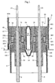
- Figs. 1 to 3 show the first embodiment of the present invention.
- designated at 1 is a grounding member
- 2 and 3 are through type capacitors
- 4 and 5 are conductors passing through the respective through type capacitors 2 and 3
- 6 is an insulating case
- 71 and 72 is an outer insulating resin
- 81 and 82 is an inner insulating resin
- 9 is an insulating cover
- 10 and 11 are insulating tubes.
- the grounding member 1 has two raised portions 101 and 102 formed on the same side. These raised portions 101 and 102 have central holes 103 and 104 respectively and are spaced apart from each other.
- the two through type capacitors 2 and 3 have through holes 201 and 301 respectively. Each capacitor also has two electrodes 202 and 203 (or 302 and 303) formed on its opposite end surfaces, where the through hole 201 (or 301) opens.
- the through type capacitors 2 and 3 are positioned on the raised portions 101 and 102 and the electrodes 203 and 303 are bonded to the raised portions 101 and 102 by means of soldering or the like.
- the capacitors 2 and 3 are made of a dielectric porcelain.
- the conductors 4 and 5 pass through the through holes 201 and 301 respectively of the capacitors 2 and 3 and are independently connected to the electrodes 202 and 302 thereof. They also pass through the holes 103 and 104 of the raised portions 101 and 102 of the grounding member 1 in a contact-free state, and their opposite end portions are led out to the outside.
- Electrode connection members used to connect the conductors 4 and 5 to electrodes 202 and 203, respectively.
- the conductors 4 and 5 have terminal sections 41 and 51 at their upper ends (in the Figure).
- the insulating case 6 has two hollow cylindrical projections 61 and 62, which are spaced apart by a distance D.
- the hollow cylindrical projections 61 and 62 have their upper open ends joined by a joining portion 64, and the insulating case has a recessed enclosure 63 in line with and following inner diameter sections 611 and 621.
- the hollow cylindrical projections 61 and 62 have their lower open end portions fitted on the outer circumferences of the raised portions 101 and 102.
- the capacitors 2 and 3 are housed within the inner diameter sections 611 and 621.
- the outer insulating resin 71 and 72 is provided around the through type capacitors 2 and 3 housed within the diameter sections 611 and 621.
- the outer insulating resin should fill in the area, not spreading too far upward or downward from the joining portion 64 of the insulating case 6.
- the inner insulating resin 81 and 82 is provided on the side of the grounding member 1 opposite the outer insulating resin 71 and 72.
- the insulating resins 71 and 72, and 81 and 82 may be composed of a thermosetting or thermoplastic resin such as a polymer with or without an inorganic filler mixed in.
- the grounding member 1 has the two raised portions 101 and 102 formed on the same side.
- the two through type capacitors 2 and 3 have the through holes 201 and 301 respectively and each capacitor has electrodes 202 and 203 (or 302 and 303) on the opposite end surfaces, where the through hole 201 (or 301) opens.
- the through type capacitors 2 and 3 are disposed on the raised portions 101 and 102 with their electrodes 203 and 303 bonded thereto.
- the conductors 4 and 5 are provided for the capacitors 2 and 3 so that they pass through the through holes 201 and 301 and are independently connected to the electrodes 202 and 302.
- This structure is thus a high voltage capacitor of independent capacitor type.
- the likelihood of separation at the interface can be reduced.
- the likelihood of withstand voltage failure can be reduced.
- the through type capacitors 2 and 3 are disposed in the hollow cylindrical projections 61 and 62 of the insulating case 6 and the outer insulating resin 71 and 72 is provided around the capacitors 2 and 3 in the inner diameter sections 611 and 621, it is possible to ensure moisture resistance and electric insulation owing to the outer insulating resin 71 and 72.
- the outer insulating resin 71 and 72 is formed by pouring a minimum necessary quantity of resin, and only into the hollow cylindrical projections 61 and 62, and the outer insulating resin 71 and 72 is independent of each other in their respective hollow cylindrical projections 61 and 62.
- a space 14 defined between the projections 61 and 62 serves as a heat radiation zone, thus reducing thermal stress generated when the high voltage capacitor of the present invention is mounted in a microwave oven or tested in heat cycle tests.
- the two hollow cylindrical projections 61 and 62 of the insulating case 6 have their upper open ends joined and their lower open end portions fitted on the outer circumferences of the raised portions 101 and 102 of the grounding member 1, it is possible to obtain a structure, in which the insulating case 6 is integrated at the top and also at the bottom as a unit.
- This has an effect of providing for increased mechanical reinforcement for the capacitors 2 and 3 and conductors 4 and 5 which are disposed in the inner diameter sections 611 and 621 of the hollow cylindrical projections 61 and 62 and thus reducing the likelihood of looseness of the conductors 4 and 5. It is thus possible to reduce the likelihood of interface separation of the conductors 4 and 5, capacitors 2 and 3 and grounding member 1 from the outer insulating resin 71 and 72 and thus greatly improve the withstand voltage characteristic.
- the insulating case 6 has the recessed enclosure 63 which is in line with and following the inner diameter sections 611 and 621 of the two hollow cylindrical projections 61 and 62, it is possible to form the outer insulating resin 71 and 72 simultaneously by pouring resin into the two hollow cylindrical projections 61 and 62 via the recessed enclosure 63. This means that the number of steps of pouring the insulating resin can be reduced by half, which leads to a cost reduction.
- the insulating case 6 has the recessed enclosure 63 which is in line with and following the inner diameter sections 611 and 621 of the two hollow cylindrical projections 61 and 62 has a flange portion 631 adjacent to the recessed enclosure.
- the flange portion 631 serves as a barrier to prevent leaks between the conductors 4 and 5 housed within and the grounding member 1.
- the grounding member 1 has two raised portions 101 and 102 formed on one side, the raised portions 101 and 102 having holes 103 and 104 respectively.
- the through type capacitors 2 and 3 have through holes 201 and 301 respectively, and each of them also has electrodes 202 and 203 (or 302 and 303) formed on its opposite end surfaces, where the through hole 201 (or 301) opens.
- the capacitors are disposed on the raised portions 101 and 102 with their electrodes 203 and 303 bonded thereto.
- the conductors 4 and 5 pass through the through holes 201 and 301 and are connected to the electrodes 202 and 302 respectively.
- the outer insulating resin 71 and 72 is composed of a thermosetting resin such as an epoxy resin or an unsaturated polyester resin, and is provided around the through type capacitors 2 and 3 on one side of the grounding member 1.
- the inner resin 81 and 82 is provided on the other side of the grounding member 1.
- the insulating case 6 is composed of a thermoplastic resin such as PBT, and is fitted on the upper end of each of the outer insulating resin 71 and 72 so that the outer insulating resin 71 and 72 is exposed between its lower end 610 and the grounding member 1.
- the insulating case 6 is made of a thermoplastic resin, its cost is low compared to a structure in which the case is made of a thermosetting resin such as an epoxy resin or an unsaturated polyester resin. Besides, since the insulating case 6 is fitted on the upper end of the outer insulating resin 71 and 72 so that the resin 71 and 72 is exposed between its lower end 610 and the grounding member 1, it can be reduced in size and its material cost.
- the outer insulating resin 71 and 72 is made of a thermosetting resin and the insulating case 6 is fitted on the upper end of the outer insulating resin 71 and 72 so that the resin 71 and 72 is exposed between its lower end 610 and the grounding member 1, the surface of the resin 71 and 72 which is made of a thermosetting resin having excellent tracking resistance characteristics, is exposed on a path which extends from the conductors 4 and 5 via the surface of the insulating case 6 to the grounding member 1.
- a high voltage capacitor and a magnetron which have excellent tracking resistance.
- Figs. 5 and 6 show examples of a manufacturing process of the second embodiment of the high voltage capacitor shown in Fig. 4.
- a case-like mold 24 is disposed on the grounding member 1 such as to surround the through type capacitors 2 and 3.
- the mold 24 composed of polypropyrene or the like. It is sealed to the grounding member 1 by press fitting or by bonding using an adhesive.
- the insulating case 6 is fitted on the upper end of the case-like mold 24.
- the outer insulating resin 71 and 72 is formed in the spaces defined by the insulating case 6 and case-like mold 24.
- the inner insulating resin 81 and 82 is formed before or after the formation of the outer insulating resin 71 and 72.
- the case-like mold 24 is removed to obtain the high voltage capacitor as shown in Fig. 4.
- Fig. 7 is a graph showing accumulative failure factor versus burn-out cycle number data of the second embodiment of the high voltage capacitor according to the invention (product according to the present invention) and a prior art high voltage capacitor (prior art product).
- the data were obtained by carrying out tests, in which the products were humidified using a supersonic humidifier. To each product was applied a secondary source voltage of a microwave oven in a cycle of being "on” for 30 seconds and then "off” for 30 seconds, and the test was continued until the insulating case surface was burnt out.
- the outer insulating resin 71 and 72 is composed of an epoxy type resin, and is provided around through type capacitors 2 and 3, and the inner insulating resin 81 and 82 is provided on the other side of grounding member 1 so that they fill the through holes 201 and 301 of the capacitors 2 and 3.
- the dielectric porcelain elements 200 and 300 constituting the capacitors 2 and 3 are covered by insulating films 204 and 304 made of an epoxy or phenol type resin.
- insulating films 204 and 304 made of an epoxy or phenol type resin covering the surfaces of the dielectric porcelain elements 200 and 300 of the through type capacitors 2 and 3
- the close contact strength and bonding strength between the dielectric porcelain 200 and 300 and the insulating resins 71 and 72, and 81 and 82 are greatly increased by the insulating films 204 and 304 covering the dielectric porcelain elements 200 and 300. It is thus possible to prevent separation or cracks from occurring in the contact interface between the dielectric porcelain elements 200 and 300 and the insulating resins 71 and 72, and 81 and 82, thus improving the reliability.
- Fig. 11 shows data obtained by actual measurement of the bonding strength between the dielectric porcelain elements 200 and 300 of the through type capacitors and the insulating resins 71 and 72, and 81 and 82.
- the Prior art product is data representing a prior art capacitor without the insulating films 204 and 304 covering the dielectric porcelain elements 200 and 300.
- the Product treated with a phenol-type undercoat is data representing a capacitor using a phenol-type resin for the insulating films 204 and 304.
- the Product treated with an epoxy-type undercoat is data representing a capacitor using an epoxy type resin for the insulating films 204 and 304.
- the average bonding strength is about 50 kgf/cm2.
- the average bonding strength is 100 kgf /cm2, while it is 150 kgf/cm2 with the product treated with epoxy type undercoat which is again a product according to the present invention.
- Fig. 12 is a diagram showing high temperature loading test data.
- the prior art product underwent electrical breakdown, presumably due to separation of the insulating resin after about 2000 hours had elapsed.
- the products treated with phenol and epoxy type undercoat as the products according to the present invention did not undergo any electrical breakdown after 3000 hours had elapsed.
- a high voltage capacitor can be obtained, which features high bonding strength, resulting in reduced likelihood of separation or cracks occurring in the insulating resin and having high durability and reliability.
- FIG. 9 Another embodiment of the high voltage capacitor according to the third aspect of the present invention will now be described with reference to Fig. 9.
- reference numerals are the same as those in the preceding Figures and designate the same parts.
- a feature of this embodiment is the fact that insulating case 6 is fitted on the upper end of the outer insulating resin 71 and 72 so that the outer insulating resin 71 and 72 is exposed between the lower end 610 of the insulating case 6 and grounding member 1.
- the insulating case 6 may be made of an inexpensive thermoplastic resin for cost reduction.
- the outer insulating resin 71 and 72 being composed of an epoxy type resin with excellent tracking resistance characteristics and being exposed on the path and extending from conductors 4 and 5 to the grounding member 1, it is possible to obtain a high voltage capacitor having excellent tracking resistance.
- Fig. 10 shows another embodiment of the high voltage capacitor according to the third aspect of the present invention.
- This embodiment comprises a single through type capacitor 2 constituted of a dielectric porcelain element 210 having two spaced-apart through holes 211 and 212.
- two independent electrodes 213 and 214 are provided so that they surround the respective through holes 211 and 212 respectively.
- a common electrode 215 is provided, which is shared by the independent electrodes 213 and 214.
- the common electrode 215 is bonded by means of soldering or the like to a raised portion 111 of the grounding member 110.
- the conductors 4 and 5 are soldered via electrode connection members 12 and 13 to the independent electrodes 213 and 214 of the through type capacitor 2.
- An insulating case 60 is fitted on the outer circumference of the raised portion 111 so as to surround the through type capacitor 2.
- An insulating cover 90 is fitted in the raised portion 111 on the other side thereof so as to surround the conductors 4 and 5.
- Insulating resin 70 and 80 are composed of a thermosetting resin, such as an epoxy type resin, and are provided on the outer and inner sides of the through type capacitor 2, which is surrounded by the insulating case 60 and the insulating cover 90.
- This high voltage capacitor has basically the same structure as the high voltage capacitor shown in Fig. 4 except that conductors 4 and 5 are not clad by any insulating tubes.
- the outer insulating resin 71 and 72 is composed of a thermosetting resin such as an epoxy or unsaturated polyester resin, and is provided around through type capacitors 2 and 3 on one side of grounding member 1.
- the inner insulating resin 81 and 82 is composed of a urethane resin, and fills through holes 201 and 301 of the through type capacitors 2 and 3 and covers the conductors 4 and 5.
- the elasticity of the inner insulating urethane resin 81 and 82 and the adhesion thereof with the porcelain elements of the through type capacitors 2 and 3 has an effect of alleviating thermal stress generated in withstand voltage tests or heat shock tests or in use.
- the conductors 4 and 5 need not be covered with insulating tubes, resulting in a reduction of the number of components and also the number of assembling steps.
- the outer insulating resin 71 and 72 may be made of a urethane resin instead of a thermosetting resin such as an epoxy or unsaturated polyester resin.
- the outer insulating resin 71 and 72 also has an effect of alleviating thermal stress generated in withstand voltage tests or heat shock tests or in use owing to the elasticity of the urethane resin and the adhesion thereof with the porcelain elements, thus permitting further reduction in cost.
- the insulating case 6 is made of a thermoplastic resin such as polybutylene telephthalate (PBT) or a thermosetting resin such as an epoxy resin. It is fitted on the upper end of the outer insulating resin 71 and 72 so that the outer insulating resin 71 and 72 is exposed between its lower end 610 and the grounding member 1.
- a thermoplastic resin such as polybutylene telephthalate (PBT) or a thermosetting resin such as an epoxy resin.
- the inner insulating resin 81 and 82 is made of a urethane resin and is provided on the side of the grounding member 1 opposite the outer insulating resin 71 and 72. Inner insulating resin 81 and inner insulating resin 82 are separated from each other by a partitioning member 91 provided on the insulating cover 9.
- the partitioning member 91 has an effect of interrupting mutual stress interference between the inner insulating resin 81 and inner insulating resin 82, thus reducing the likelihood of interface separation of the conductors 4 and 5 and insulating cover 9 from the inner insulating resin 81 and 82.
- the fourth aspect of the present invention can be applied broadly to the high voltage capacitors having the structures shown in Figs. 1 through 10.
- Fig. 14 shows heat shock test data obtained from an embodiment of the fourth aspect of the present invention.
- Sample 1 is a prior art product, which has conductors clad with insulating tubes of silicone rubber and inner insulating resin composed of an epoxy resin.
- Sample 2 is a product, which has bare conductors, i.e., conductors without any silicone rubber insulating tube covering them, and inner insulating resin composed of an epoxy resin.
- Sample 3 is a product according to the present invention, which has conductors without any silicone rubber insulating tube cover and inner insulating resin composed of a urethane resin.
- the heat shock test was conducted by setting a cycle pattern of one hour at - 40°C and followed by one hour at 120 °C. An AC withstand voltage test was conducted for every 10 cycles of this pattern.
- Sample 3 which is a product according to the present invention, has heat shock resistance characteristics comparable to that of Sample 1, which is a prior art product.
- Sample 2 which has conductors without any silicone rubber insulating tubes and inner insulating resin composed of an epoxy resin, withstand voltage failure due to heat shock takes place after about 10 cycles.
- Designated at 70 is the outer insulating resin, and at 80 the inner insulating resin.
- the outer insulating resin 70 is provided around through type capacitor 2 on one side of grounding member 1, and its entire outer circumference constitutes a space-partitioning contour.
- the inner insulating resin 80 fills through holes 211 and 212 of the through type capacitor 2 on the other side of the grounding member 1. Its entire outer circumference also has a space-partitioning contour.
- outer insulating resin 70 and the inner insulating resin 80 also serve as outer fittings, and therefore, neither an insulating case nor an insulating cover is required. This means that there is no cause for separation of the outer and inner insulating resins 70 and 80 from the dielectric porcelain element 210 due to temperature variations in heat shock tests or heat cycle tests or in use. It is thus possible to prevent separation, gaps or cracks from occurring at the contact interface between the dielectric porcelain element 210 of the through type capacitor 2 and the outer insulating resin 70 and the inner insulating resin 80.
- the outer insulating resin 70 and and the inner insulating resin 80 can be formed by injection molding. It is thus possible to prevent defective products being produced due to otherwise possible flow-out of the insulating resin to the outside.
- the outer insulating resin 70 has a recessed enclosure 701, through which conductors 4 and 5 are led out, and also has a frame portion 702 defining the recessed enclosure 701.
- the inner insulating resin 80 has a recessed enclosure 801, through which the conductors 4 and 5 are led out, and also has a frame portion 802 defining the recessed enclosure 801.
- Fig. 16 shows another embodiment of the high voltage capacitor according to the fifth aspect of the present invention.
- the outer circumference of the outer insulating resin 70 has fins 703. With this structure, it is possible to increase the creeping distance from the conductors 4 and 5 to the grounding member 1.
- Fig. 17 shows yet another embodiment of the high voltage capacitor according to the fifth aspect of the present invention.
- the grounding member 1 has two raised portions 101 and 102 formed on the same side.
- the raised portions 101 and 102 have respective central holes 103 and 104 and are spaced apart from each other.
- Two through type capacitors 200 and 300 are each disposed on each of the raised portions 101 and 102. They have dielectric porcelain elements 200 and 300 respectively and through holes 201 and 301 in the dielectric porcelain elements. Furthermore, they each have pair electrodes 202 and 203 or 302 and 303 formed on the end surfaces, where the through holes 202 and 203 or 302 and 303 open. The electrodes 203 and 303 are bonded by means of soldering or the like to the raised portions 101 and 102.
- the conductors 4 and 5 pass through the through holes 201 and 301 respectively of the through type capacitors 20 and 30 and are connected independently to the electrodes 202 and 203. They pass through holes 103, 104 formed in the raised portions 101 and 102 of the grounding member 1 in a contact-free state and their opposite end portions are led out to the outside.
- outer insulating resin 70 and inner insulating resin 80 are formed so that they are continuous to each other at the through type capacitors 20 and 30, and their entire outer circumferences constitute space-partitioning contours. Alternatively, they may be formed so that they are independent of each other at the through type capacitors 20 and 30.
- Fig. I8 shows yet another embodiment of the high voltage capacitor according to the fifth aspect of the present invention.
- an insulating partitioning member 704 is disposed in outer insulating resin 70 between through type capacitors 20 and 30.
- the outer insulating resin 70 is divided into two parts, one on the side of the through hole capacitor 20 and the other on the side of the through type capacitor 30, mutual stress interaction can be reduced for more effectively preventing the separation, gaps or cracks from occurring in the contact interface between the through type capacitors 20 and 30 and the outer insulating resin 70.
- This embodiment of the high voltage capacitor has basically the same structure as the high voltage capacitor shown in Figs. 1 and 8.
- the insulating resins 71 and 72, 81 and 82 are formed around through type capacitors 20 and 30 so that they are in close contact with dielectric porcelain elements 200 and 300.
- dielectric porcelain elements 200 and 300 which constitute the through type capacitors 20 and 30 have a surface grain size of 2 to 5 ⁇ m, which is much larger than than of prior art dielectric porcelain elements.
- the dielectric porcelain elements 200 and 300 have a surface roughness of 0.2 ⁇ m or above.
- Figs. 20 and 21 respectively show surface roughness curves of a dielectric porcelain element used for a prior art high voltage capacitor and that used for the sixth embodiment of the high voltage capacitor according to the sixth aspect of the present invention.
- the surface roughness Ra is 0.14 ⁇ m
- Ra is 0.25 ⁇ m.
- Fig. 22 shows actual measured data on the bonding strength. As shown in the Figure, in a measurement temperature range of 80 to 140°C, the bonding strength, which was about 20 to 40 kgf/cm2 with the prior art product, is increased up to about 40 to 60 kgf/cm2.
- the likelihood of separation, gaps or cracks occurring in the contact interface between the dielectric porcelain element of the through type capacitor and the insulating resin due to temperature changes in heat shock tests or heat cycle tests or in use is reduced.
- the reliability of the high voltage capacitor in reliability tests such as high temperature loading tests or moisture resistance loading tests or in use in high temperature, high relative humidity environments is greatly improved.
- Fig. 23 shows the results of high temperature loading tests.
- the tests were conducted by taking out a suitable number of products according to the present invention and prior art products and applying a high DC voltage of 15kv to them under a temperature condition of 120°C.
- a high DC voltage of 15kv was applied to them under a temperature condition of 120°C.
- electric breakdown took place after 3, 6, 16, 22 and 500 hours had elapsed, presumably due to separation of the insulating resin.
- electric breakdown did not take place even after 2000 hours had elapsed. This is owing to a significant improvement in reliability in reliability tests such as high temperature loading tests or moisture resistance loading tests or in use under high temperature, high relative humidity conditions.
- Fig. 24 shows another embodiment of the high voltage capacitor according to the sixth aspect of the present invention.
- reference numerals are the same those in the preceding Figures and designate parts substantially the same.
- the insulating case 6 has a joining portion 64, which is embedded in the outer insulating resin 7.
- the sixth aspect of the present invention is broadly applicable to the high voltage capacitors shown in Figs. I through 23.
- This embodiment of the high voltage capacitor has basically the same structure as the high voltage capacitors shown in Figs. I, 8 and 19.
- the outer insulating resin 71 and 72 or the inner insulating resin 81 and 82 is composed of a urethane resin.
- the outer insulating resin 71 and 72 is made of a thermosetting resin such as an epoxy or unsaturated polyester resin and is formed around through type capacitors 20 and 30 on one side of grounding member 1. It is in close contact with dielectric porcelain elements 200 and 300.
- the inner insulating resin 81 and 82 is made of a urethane resin and formed so as to fill through holes 201 and 301 of the through type capacitors 20 and 30. It is in close contact with the dielectric porcelain elements 200 and 300.
- the insulating tubes 10 and 11 cover the portions of conductors 4 and 5 passing through the through holes 201 and 301.
- the elasticity of the urethane resin and the adhesion thereof with the dielectric porcelain elements 200 and 300 have an effect of reducing the likelihood of separation, gaps or cracks occurring in the contact interface between the inner insulating resin 8I and 82 and dielectric porcelain 200 and 300 due to thermal stress generated in heat cycle tests or heat shock tests or in use.
- the reliability in reliability tests such as high temperature loading tests or moisture resistance loading tests or in use in high temperature, high relative humidity environments is greatly improved.
- the elasticity of the insulating tubes 10 and 11 and the elasticity of the urethane resin have a combined effect of further reducing the likelihood of separation in the contact interface between the dielectric porcelain elements 200 and 300 and the inner insulating resin 81 and 82.
- the outer insulating resin 71 and 72 is made of a urethane resin
- the elasticity of the urethane resin and the adhesion thereof to the dielectric porcelain elements 200 and 300 likewise have an effect of reducing the likelihood of separation, gaps or cracks occurring in the contact interface between the insulating resin 71 and 72 and the dielectric porcelain 200 and 300 due to thermal stress generated in heat cycle tests or heat shock tests or in use, thus greatly improving reliability in reliability tests such as high temperature loading tests, moisture resistance loading tests or in use in high temperature, high relative humidity environments.
- Fig. 26 shows the results of high temperature loading tests.
- the tests were conducted by taking out a suitable number of samples of the product according to the present invention and those of the prior art product and applying a high DC voltage of 15kv to them under a temperature condition of 120°C.
- the tested product according to the present invention was prepared by using a urethane resin for the outer and inner insulating resins 71 and 72, 81 and 82.
- the accumulative failure factor reaches 90 % after 3500 hours, whereas with the product according to the present invention it reaches 90 % after 7000 hours, thus showing double the life of the prior art product.
- Fig. 27 shows results of heat shock tests. The tests were conducted by taking out a suitable number of samples of the product according to the present invention and those of the prior art product. Each sample was given a heat shock in a cycle pattern of one hour at 120 °C and then one hour at-40°C. A voltage breakdown test was conducted for every 10 cycles, and electric breakdown, presumably due to separation was checked for. As shown in the Figure, with the prior art product the accumulative failure factor reaches 90 % after 350 cycles, whereas with the product according to the present invention it reaches 90 % after 1000 cycles, thus showing triple the life of the prior art product.
- Fig. 28 shows the results of moisture resistance tests.
- the tests were conducted by taking out a suitable number of samples of the product according to the present invention and those of the prior art product. Each sample was left in an atmosphere at a temperature of 40°C and under a relative humidity of 90 to 95 % RH, and withstand voltage tests were conducted after 240, 500, 1000, 1500, 2000, 3000, 4000 and 5000 hours had elapsed to check for electric breakdown presumably due to separation.
- failure occurred after 1500 and 2000 hours, whereas with the product according to the present invention no failure was detected even after 5000 hours.
- the seventh aspect of the present invention is also broadly applicable to high voltage capacitors having various structures, for instance the high voltage capacitors shown in Figs. 1 through 24.
- Fig. 29 is a partial cut-away section of a magnetron which has the high-voltage capacitor of the present invention fitted as a filter.
- Reference numeral 15 indicates the cathode stem, 16 the filter box, 17 and 18 inductors and 19 the high-voltage capacitor of the present invention.
- the high-voltage capacitor 19 functions as a filter along with inductors 17 and 18.
- the filter box 16 is placed so that it covers the cathode stem 15, and the high-voltage capacitor 19 passes through the through hole created in the side plate 161 of the filter box 16 so that the outer insulating resin 70 is exposed to the outside. It is mounted and bonded on to the side plate 161 of the filter box 16 with the grounding member 1.
- the inductors 17 and 18 are directly connected between the cathode terminal of the cathode stem 15 and the conductors 4 and 5 of the high-voltage capacitor 19 inside the filter box 16.
- Reference numeral 21 indicates cooling fins, 22 a gasket, 23 the RF output terminal and 24 indicates a magnet.
- the grounding member has two raised portions formed on the same side
- the two through type capacitors with through holes are disposed on the raised portions and each has two electrodes formed on the opposite surfaces, where the through hole opens, one of the two electrodes is bonded to the raised portion, and the conductors passing through the through holes of the respective through type capacitors are independently connected to the other electrodes thereof.
- the two through type capacitors are accommodated within the inner diameter sections of the respective hollow cylindrical projections of the insulating case, and the insulating resin is provided around through type capacitors thus accommodated, it is possible to pour a minimum necessary amount of insulating resin into the individual hollow cylindrical projections and substantially independently between the same.
- the two hollow cylindrical projections of the insulating case are joined and have their lower open end fitted on the outer circumference of the raised portions of the grounding member, it is possible to provide a high voltage capacitor and a magnetron of high quality and high reliability, which the mechanical strength of the through type capacitors and conductors accommodated in the inner spaces of the hollow cylindrical projections is fortified thus preventing interface separation of the conductors, through type capacitors and grounding member from the insulating resin due to otherwise possible looseness of the conductors, thus greatly improving the withstand voltage characteristics.
- the insulating case has a recessed enclosure formed at the upper open ends of the two hollow cylindrical projections in line with and following the inner diameter sections, it is possible to provide a high voltage capacitor and a magnetron, which permits reduction in the number of insulating resin pouring steps by one half and thus permits cost reduction.
- the upper open ends of the two hollow cylindrical projections form a recessed enclosure in line with and following the inner diameter sections, it is possible to provide a high voltage capacitor and a magnetron with superior withstand voltage characteristics under humid conditions, and which can be used successfully in environments of high relative humidity or with much dust.
- the two hollow cylindrical projections of the insulating case are spaced apart, the space created between the projections constitutes a heat radiation zone, and thus it is possible to provide a high voltage capacitor and a magnetron, in which less thermal stress is generated in use in a microwave oven or in heat cycle tests, and which thus has reduced likelihood of the withstand voltage failure.
- the insulating case is made of a thermoplastic resin, it is possible to provide a high voltage capacitor and a magnetron, which are inexpensive compared to a structure using a thermosetting resin such as an epoxy or unsaturated polyester resin.
- the insulating case is fitted on the upper end of the outer insulating resin so as to expose the outer insulating resin between its lower end and the grounding member, it is possible to provide a high voltage capacitor and a magnetron, which have a smaller insulating case and reduced material costs.
- the outer insulating resin is made of a thermosetting resin and the insulating case is fitted on the upper end of the outer insulating resin so as to expose the outer insulating resin between its lower end and the grounding member, it is possible to provide a high voltage capacitor and a magnetron, in which the surface of the outer insulating resin composed of a thermosetting resin having excellent tracking resistance characteristics is exposed on a path leading from the conductors along the surface of the insulating case to the grounding member, and which thus is superior in tracking resistance and humid-conditions withstand voltage characteristics.
- the outer insulating resin is made of an epoxy type resin and provided around the through hole capacitors, and the dielectric porcelain elements thereof are covered by an insulating film of an epoxy or phenol type resin.
- the close adhesion and bonding strength between the dielectric porcelain elements and the insulating resin are greatly increased by the insulating film covering the dielectric porcelain elements.
- the insulating resin consists of an outer insulating resin and an inner insulating resin, and at least either the outer insulating resin or the inner insulating resin is made of a urethane resin, the outer insulating resin is provided around the through type capacitors on one side of the grounding member, and the inner insulating resin is provided to fill the through holes of the through type capacitors on the other side of the grounding member.
- the outer insulating resin is provided around the through type capacitor on one side of the grounding member, and its entire outer circumference constitutes a space -partitioning contour and the inner insulating resin fills the through holes of the through type capacitor on the other side of the grounding member, and its entire outer circumference constitutes a space-partitioning contour, the outer insulating resin and the inner insulating resin thus serve as outer fittings, thus permitting dispensing with the heretofore necessary insulating case and insulating cover.
- the dielectric porcelain elements constituting the through type capacitors have a surface grain size of 2 to 5 ⁇ m and a surface roughness of 0.2 ⁇ m or more the bonding strength between the dielectric porcelain elements and the insulating resin is increased from the prior art value of 20 to 40 kgf/cm2 up to about 40 to 60 kgf/cm2.
- the outer insulating resin or inner insulating resin is made of a urethane resin, it is possible to provide a high voltage capacitor and a magnetron, in which, at least on the side provided with the urethane resin, the likelihood of separation, gaps or cracks occurring in the contact interface between the dielectric porcelain of the through type capacitors and the insulating resin due to thermal stress in heat cycle tests or heat shock tests or in use can be reduced owing to the elasticity of the urethane resin and the adhesion thereof with the dielectric porcelain, thus greatly improving reliability in reliability tests such as high temperature loading tests or moisture resistance tests or in use in high temperature, high relative humidity environments.
- the insulating tubes are made of an elastic resin and cover the portions of the conductors passing through the through holes of the through type capacitors, by using a urethane resin for the inner insulating resin, it is possible to provide a high voltage capacitor and a magnetron, in which the elasticity of the insulating tubes and the elasticity of the urethane resin have a combined effect of reducing the likelihood of separation, gaps or cracks occurring in the contact interface between the dielectric porcelain elements and the inner insulating resin.
Abstract
Applications Claiming Priority (13)
| Application Number | Priority Date | Filing Date | Title |
|---|---|---|---|
| JP1991075727U JP2571361Y2 (ja) | 1991-08-27 | 1991-08-27 | 高電圧コンデンサ及びマグネトロン |
| JP75727/91U | 1991-08-27 | ||
| JP7715691U JPH0521431U (ja) | 1991-08-29 | 1991-08-29 | 高電圧コンデンサ及びマグネトロン |
| JP77156/91U | 1991-08-29 | ||
| JP1991080035U JP2580628Y2 (ja) | 1991-09-05 | 1991-09-05 | 高電圧コンデンサ及びマグネトロン |
| JP80035/91U | 1991-09-05 | ||
| JP082301U JPH0525718U (ja) | 1991-09-12 | 1991-09-12 | 高電圧コンデンサ及びマグネトロン |
| JP82301/91U | 1991-09-12 | ||
| JP085423U JPH0623238U (ja) | 1991-09-24 | 1991-09-24 | 高電圧コンデンサ及びマグネトロン |
| JP85423/91U | 1991-09-24 | ||
| JP9058091U JPH0533519U (ja) | 1991-10-08 | 1991-10-08 | 高電圧コンデンサ及びマグネトロン |
| JP90580/91U | 1991-10-08 | ||
| PCT/JP1992/001077 WO1993004494A1 (fr) | 1991-08-27 | 1992-08-26 | Condensateur haute tension et magnetron |
Publications (3)
| Publication Number | Publication Date |
|---|---|
| EP0604652A1 true EP0604652A1 (fr) | 1994-07-06 |
| EP0604652A4 EP0604652A4 (fr) | 1994-12-07 |
| EP0604652B1 EP0604652B1 (fr) | 1998-07-01 |
Family
ID=27551343
Family Applications (1)
| Application Number | Title | Priority Date | Filing Date |
|---|---|---|---|
| EP92918700A Expired - Lifetime EP0604652B1 (fr) | 1991-08-27 | 1992-08-26 | Condensateur haute tension et magnetron |
Country Status (7)
| Country | Link |
|---|---|
| US (1) | US5544002A (fr) |
| EP (1) | EP0604652B1 (fr) |
| AU (1) | AU664383B2 (fr) |
| BR (1) | BR9206431A (fr) |
| CA (1) | CA2116571C (fr) |
| DE (1) | DE69226084T2 (fr) |
| WO (1) | WO1993004494A1 (fr) |
Cited By (2)
| Publication number | Priority date | Publication date | Assignee | Title |
|---|---|---|---|---|
| EP1035554A2 (fr) * | 1999-03-05 | 2000-09-13 | TDK Corporation | Condensateur à haute tension et micro-ondes |
| EP1551042A1 (fr) * | 2003-12-30 | 2005-07-06 | Lg Electronics Inc. | Condensateur haute tension pour magnétron |
Families Citing this family (16)
| Publication number | Priority date | Publication date | Assignee | Title |
|---|---|---|---|---|
| US5910879A (en) * | 1996-06-27 | 1999-06-08 | Herbert; Edward | 3- and 4-terminal capacitors with "Faraday-shielded" connections |
| JPH1092693A (ja) * | 1996-09-18 | 1998-04-10 | Tdk Corp | 貫通型セラミックコンデンサ |
| JPH10149948A (ja) * | 1996-11-19 | 1998-06-02 | Tdk Corp | 高電圧貫通形コンデンサ |
| US7042703B2 (en) * | 2000-03-22 | 2006-05-09 | X2Y Attenuators, Llc | Energy conditioning structure |
| US9054094B2 (en) | 1997-04-08 | 2015-06-09 | X2Y Attenuators, Llc | Energy conditioning circuit arrangement for integrated circuit |
| US6469595B2 (en) * | 2000-03-22 | 2002-10-22 | X2Y Attenuators, Llc | Isolating energy conditioning shield assembly |
| US7336468B2 (en) | 1997-04-08 | 2008-02-26 | X2Y Attenuators, Llc | Arrangement for energy conditioning |
| US7301748B2 (en) | 1997-04-08 | 2007-11-27 | Anthony Anthony A | Universal energy conditioning interposer with circuit architecture |
| US7321485B2 (en) | 1997-04-08 | 2008-01-22 | X2Y Attenuators, Llc | Arrangement for energy conditioning |
| JP3803258B2 (ja) * | 2000-04-03 | 2006-08-02 | Tdk株式会社 | 高電圧貫通型コンデンサ及びマグネトロン |
| JP2005109006A (ja) * | 2003-09-29 | 2005-04-21 | Tdk Corp | 高電圧貫通型コンデンサ及びマグネトロン |
| US7675729B2 (en) | 2003-12-22 | 2010-03-09 | X2Y Attenuators, Llc | Internally shielded energy conditioner |
| WO2006093831A2 (fr) | 2005-03-01 | 2006-09-08 | X2Y Attenuators, Llc | Conditionneur d'energie avec electrodes traversantes reliees |
| GB2439862A (en) | 2005-03-01 | 2008-01-09 | X2Y Attenuators Llc | Conditioner with coplanar conductors |
| EP1991996A1 (fr) | 2006-03-07 | 2008-11-19 | X2Y Attenuators, L.L.C. | Structures de conditionneur d'énergie |
| JP2023016193A (ja) * | 2021-07-21 | 2023-02-02 | Tdk株式会社 | 高電圧貫通型コンデンサ |
Citations (2)
| Publication number | Priority date | Publication date | Assignee | Title |
|---|---|---|---|---|
| DE3029807A1 (de) * | 1979-08-15 | 1981-02-26 | Tdk Electronics Co Ltd | Keramischer doppel-durchfuehrungskondensator |
| EP0259766A2 (fr) * | 1986-09-11 | 1988-03-16 | TDK Corporation | Condensateur du type traversée et magnétron l'utilisant |
Family Cites Families (10)
| Publication number | Priority date | Publication date | Assignee | Title |
|---|---|---|---|---|
| JPS5930521Y2 (ja) * | 1979-10-01 | 1984-08-31 | ティーディーケイ株式会社 | 高電圧貫通形コンデンサ |
| US4370698A (en) * | 1979-10-08 | 1983-01-25 | Tdk Electronics Co., Ltd. | Through type high-withstand-voltage ceramic |
| JPS5930522Y2 (ja) * | 1979-10-13 | 1984-08-31 | ティーディーケイ株式会社 | 高電圧貫通形コンデンサ |
| JPS6175119U (fr) * | 1984-10-23 | 1986-05-21 | ||
| JPH0423310Y2 (fr) * | 1986-08-05 | 1992-05-29 | ||
| JPS6370137U (fr) * | 1986-10-27 | 1988-05-11 | ||
| JPH0525224Y2 (fr) * | 1987-04-20 | 1993-06-25 | ||
| US5032949A (en) * | 1988-06-07 | 1991-07-16 | Tdk Corporation | High-voltage through-type ceramic capacitor |
| JP2804532B2 (ja) * | 1988-09-20 | 1998-09-30 | 三洋電機株式会社 | 高圧用貫通形コンデンサおよびその製造方法 |
| JPH0254217U (fr) * | 1988-10-12 | 1990-04-19 |
-
1992
- 1992-08-26 EP EP92918700A patent/EP0604652B1/fr not_active Expired - Lifetime
- 1992-08-26 AU AU25012/92A patent/AU664383B2/en not_active Ceased
- 1992-08-26 DE DE69226084T patent/DE69226084T2/de not_active Expired - Fee Related
- 1992-08-26 BR BR9206431A patent/BR9206431A/pt not_active IP Right Cessation
- 1992-08-26 CA CA002116571A patent/CA2116571C/fr not_active Expired - Fee Related
- 1992-08-26 US US08/196,229 patent/US5544002A/en not_active Expired - Lifetime
- 1992-08-26 WO PCT/JP1992/001077 patent/WO1993004494A1/fr active IP Right Grant
Patent Citations (2)
| Publication number | Priority date | Publication date | Assignee | Title |
|---|---|---|---|---|
| DE3029807A1 (de) * | 1979-08-15 | 1981-02-26 | Tdk Electronics Co Ltd | Keramischer doppel-durchfuehrungskondensator |
| EP0259766A2 (fr) * | 1986-09-11 | 1988-03-16 | TDK Corporation | Condensateur du type traversée et magnétron l'utilisant |
Non-Patent Citations (1)
| Title |
|---|
| See also references of WO9304494A1 * |
Cited By (4)
| Publication number | Priority date | Publication date | Assignee | Title |
|---|---|---|---|---|
| EP1035554A2 (fr) * | 1999-03-05 | 2000-09-13 | TDK Corporation | Condensateur à haute tension et micro-ondes |
| EP1035554A3 (fr) * | 1999-03-05 | 2003-12-10 | TDK Corporation | Condensateur à haute tension et micro-ondes |
| EP1551042A1 (fr) * | 2003-12-30 | 2005-07-06 | Lg Electronics Inc. | Condensateur haute tension pour magnétron |
| US7123464B2 (en) | 2003-12-30 | 2006-10-17 | Lg Electronics Inc. | High voltage input apparatus for magnetron |
Also Published As
| Publication number | Publication date |
|---|---|
| CA2116571A1 (fr) | 1993-03-04 |
| DE69226084D1 (de) | 1998-08-06 |
| US5544002A (en) | 1996-08-06 |
| CA2116571C (fr) | 2000-11-14 |
| AU664383B2 (en) | 1995-11-16 |
| EP0604652A4 (fr) | 1994-12-07 |
| BR9206431A (pt) | 1994-08-02 |
| AU2501292A (en) | 1993-03-16 |
| DE69226084T2 (de) | 1998-12-24 |
| WO1993004494A1 (fr) | 1993-03-04 |
| EP0604652B1 (fr) | 1998-07-01 |
Similar Documents
| Publication | Publication Date | Title |
|---|---|---|
| US5544002A (en) | High voltage capacitor and magnetron | |
| CA1123035A (fr) | Borne hermetique de moteur de compresseur | |
| US4768129A (en) | Through type twin capacitor | |
| KR920007980B1 (ko) | 관통형 커패시터 및 그를 이용한 마그네트론 | |
| JPH081877B2 (ja) | 貫通形キャパシタ | |
| US5113309A (en) | High-voltage through-type ceramic capacitor | |
| KR910004727B1 (ko) | 고압 입력단자를 구비한 전자레인지용 마그네트론 | |
| US20230039264A1 (en) | Metal case capacitor | |
| KR20000062751A (ko) | 고전압 콘덴서 및 마그네트론 | |
| US4558399A (en) | Electrolytic capacitor and a process for producing the same | |
| JP3139914B2 (ja) | モールド形変流器 | |
| JPH0423310Y2 (fr) | ||
| KR100264912B1 (ko) | 고전압 커패시터 및 자전관 | |
| JP2580629Y2 (ja) | 高電圧コンデンサ及びマグネトロン | |
| US2285594A (en) | Bushing cap | |
| JPH0528021U (ja) | 高電圧コンデンサ及びマグネトロン | |
| JP2561721Y2 (ja) | 高電圧コンデンサ及びマグネトロン | |
| JPH0423312Y2 (fr) | ||
| JPH0423311Y2 (fr) | ||
| JP3229772B2 (ja) | 高電圧抵抗パック | |
| CN117711819A (zh) | 电容器 | |
| JP2571361Y2 (ja) | 高電圧コンデンサ及びマグネトロン | |
| JPH07105287B2 (ja) | 高電圧抵抗パック及びその製造方法 | |
| JPH0539549Y2 (fr) | ||
| JP2580628Y2 (ja) | 高電圧コンデンサ及びマグネトロン |
Legal Events
| Date | Code | Title | Description |
|---|---|---|---|
| PUAI | Public reference made under article 153(3) epc to a published international application that has entered the european phase |
Free format text: ORIGINAL CODE: 0009012 |
|
| 17P | Request for examination filed |
Effective date: 19940218 |
|
| AK | Designated contracting states |
Kind code of ref document: A1 Designated state(s): DE FR GB IT NL |
|
| A4 | Supplementary search report drawn up and despatched | ||
| AK | Designated contracting states |
Kind code of ref document: A4 Designated state(s): DE FR GB IT NL |
|
| 17Q | First examination report despatched |
Effective date: 19960729 |
|
| GRAG | Despatch of communication of intention to grant |
Free format text: ORIGINAL CODE: EPIDOS AGRA |
|
| GRAG | Despatch of communication of intention to grant |
Free format text: ORIGINAL CODE: EPIDOS AGRA |
|
| GRAH | Despatch of communication of intention to grant a patent |
Free format text: ORIGINAL CODE: EPIDOS IGRA |
|
| GRAH | Despatch of communication of intention to grant a patent |
Free format text: ORIGINAL CODE: EPIDOS IGRA |
|
| GRAA | (expected) grant |
Free format text: ORIGINAL CODE: 0009210 |
|
| AK | Designated contracting states |
Kind code of ref document: B1 Designated state(s): DE FR GB IT NL |
|
| REF | Corresponds to: |
Ref document number: 69226084 Country of ref document: DE Date of ref document: 19980806 |
|
| ET | Fr: translation filed | ||
| PLBE | No opposition filed within time limit |
Free format text: ORIGINAL CODE: 0009261 |
|
| STAA | Information on the status of an ep patent application or granted ep patent |
Free format text: STATUS: NO OPPOSITION FILED WITHIN TIME LIMIT |
|
| 26N | No opposition filed | ||
| REG | Reference to a national code |
Ref country code: GB Ref legal event code: IF02 |
|
| PGFP | Annual fee paid to national office [announced via postgrant information from national office to epo] |
Ref country code: DE Payment date: 20070823 Year of fee payment: 16 |
|
| PGFP | Annual fee paid to national office [announced via postgrant information from national office to epo] |
Ref country code: GB Payment date: 20070822 Year of fee payment: 16 |
|
| PGFP | Annual fee paid to national office [announced via postgrant information from national office to epo] |
Ref country code: NL Payment date: 20070805 Year of fee payment: 16 Ref country code: IT Payment date: 20070828 Year of fee payment: 16 |
|
| PGFP | Annual fee paid to national office [announced via postgrant information from national office to epo] |
Ref country code: FR Payment date: 20070808 Year of fee payment: 16 |
|
| GBPC | Gb: european patent ceased through non-payment of renewal fee |
Effective date: 20080826 |
|
| NLV4 | Nl: lapsed or anulled due to non-payment of the annual fee |
Effective date: 20090301 |
|
| PG25 | Lapsed in a contracting state [announced via postgrant information from national office to epo] |
Ref country code: NL Free format text: LAPSE BECAUSE OF NON-PAYMENT OF DUE FEES Effective date: 20090301 |
|
| REG | Reference to a national code |
Ref country code: FR Ref legal event code: ST Effective date: 20090430 |
|
| PG25 | Lapsed in a contracting state [announced via postgrant information from national office to epo] |
Ref country code: IT Free format text: LAPSE BECAUSE OF NON-PAYMENT OF DUE FEES Effective date: 20080826 Ref country code: FR Free format text: LAPSE BECAUSE OF NON-PAYMENT OF DUE FEES Effective date: 20080901 Ref country code: DE Free format text: LAPSE BECAUSE OF NON-PAYMENT OF DUE FEES Effective date: 20090303 |
|
| PG25 | Lapsed in a contracting state [announced via postgrant information from national office to epo] |
Ref country code: GB Free format text: LAPSE BECAUSE OF NON-PAYMENT OF DUE FEES Effective date: 20080826 |