EP0573014A2 - Tintenstrahlkopfherstellungsverfahren, nach dem Verfahren hergestellter Tintenstrahlkopf und Tintenstrahlgerät damit versehen - Google Patents
Tintenstrahlkopfherstellungsverfahren, nach dem Verfahren hergestellter Tintenstrahlkopf und Tintenstrahlgerät damit versehen Download PDFInfo
- Publication number
- EP0573014A2 EP0573014A2 EP93108875A EP93108875A EP0573014A2 EP 0573014 A2 EP0573014 A2 EP 0573014A2 EP 93108875 A EP93108875 A EP 93108875A EP 93108875 A EP93108875 A EP 93108875A EP 0573014 A2 EP0573014 A2 EP 0573014A2
- Authority
- EP
- European Patent Office
- Prior art keywords
- substrate
- solid layer
- formation
- ink
- ink jet
- Prior art date
- Legal status (The legal status is an assumption and is not a legal conclusion. Google has not performed a legal analysis and makes no representation as to the accuracy of the status listed.)
- Granted
Links
- 238000000034 method Methods 0.000 title claims abstract description 161
- 238000004519 manufacturing process Methods 0.000 title claims abstract description 45
- 239000007787 solid Substances 0.000 claims abstract description 217
- 239000000758 substrate Substances 0.000 claims abstract description 184
- 230000015572 biosynthetic process Effects 0.000 claims abstract description 167
- 239000007788 liquid Substances 0.000 claims abstract description 153
- 229920005989 resin Polymers 0.000 claims abstract description 112
- 239000011347 resin Substances 0.000 claims abstract description 112
- 238000007599 discharging Methods 0.000 claims abstract description 110
- 230000008569 process Effects 0.000 claims abstract description 52
- 238000009835 boiling Methods 0.000 claims description 4
- 238000005520 cutting process Methods 0.000 abstract description 21
- 239000010410 layer Substances 0.000 description 204
- 239000000463 material Substances 0.000 description 49
- 238000012546 transfer Methods 0.000 description 38
- HEMHJVSKTPXQMS-UHFFFAOYSA-M Sodium hydroxide Chemical compound [OH-].[Na+] HEMHJVSKTPXQMS-UHFFFAOYSA-M 0.000 description 33
- 239000002904 solvent Substances 0.000 description 30
- 238000010438 heat treatment Methods 0.000 description 13
- 239000007924 injection Substances 0.000 description 13
- 238000002347 injection Methods 0.000 description 13
- 230000005855 radiation Effects 0.000 description 13
- CSCPPACGZOOCGX-UHFFFAOYSA-N Acetone Chemical compound CC(C)=O CSCPPACGZOOCGX-UHFFFAOYSA-N 0.000 description 12
- 239000007864 aqueous solution Substances 0.000 description 12
- 235000012431 wafers Nutrition 0.000 description 12
- 238000011161 development Methods 0.000 description 11
- 230000018109 developmental process Effects 0.000 description 11
- 235000011121 sodium hydroxide Nutrition 0.000 description 11
- 230000008901 benefit Effects 0.000 description 10
- 238000011084 recovery Methods 0.000 description 10
- XUIMIQQOPSSXEZ-UHFFFAOYSA-N Silicon Chemical compound [Si] XUIMIQQOPSSXEZ-UHFFFAOYSA-N 0.000 description 9
- 239000002245 particle Substances 0.000 description 9
- 230000001681 protective effect Effects 0.000 description 9
- 229910052710 silicon Inorganic materials 0.000 description 9
- 239000003822 epoxy resin Substances 0.000 description 8
- 229920000647 polyepoxide Polymers 0.000 description 8
- 239000010703 silicon Substances 0.000 description 8
- 238000000465 moulding Methods 0.000 description 7
- 238000012545 processing Methods 0.000 description 7
- 229910003862 HfB2 Inorganic materials 0.000 description 6
- 238000013019 agitation Methods 0.000 description 6
- 229910052782 aluminium Inorganic materials 0.000 description 6
- 230000000694 effects Effects 0.000 description 6
- 238000005530 etching Methods 0.000 description 6
- 229910052751 metal Inorganic materials 0.000 description 6
- 239000002184 metal Substances 0.000 description 6
- 239000003960 organic solvent Substances 0.000 description 6
- 238000011417 postcuring Methods 0.000 description 6
- 238000004544 sputter deposition Methods 0.000 description 6
- 239000000853 adhesive Substances 0.000 description 5
- 230000001070 adhesive effect Effects 0.000 description 5
- 239000011248 coating agent Substances 0.000 description 5
- 238000000576 coating method Methods 0.000 description 5
- 238000000151 deposition Methods 0.000 description 5
- 230000008021 deposition Effects 0.000 description 5
- 238000009998 heat setting Methods 0.000 description 5
- 230000001737 promoting effect Effects 0.000 description 5
- 239000004065 semiconductor Substances 0.000 description 5
- 230000003466 anti-cipated effect Effects 0.000 description 4
- 239000000428 dust Substances 0.000 description 4
- 238000000206 photolithography Methods 0.000 description 4
- 238000007650 screen-printing Methods 0.000 description 4
- XAGFODPZIPBFFR-UHFFFAOYSA-N aluminium Chemical compound [Al] XAGFODPZIPBFFR-UHFFFAOYSA-N 0.000 description 3
- 230000008602 contraction Effects 0.000 description 3
- 239000011521 glass Substances 0.000 description 3
- 239000002346 layers by function Substances 0.000 description 3
- 230000007246 mechanism Effects 0.000 description 3
- VYPSYNLAJGMNEJ-UHFFFAOYSA-N Silicium dioxide Chemical compound O=[Si]=O VYPSYNLAJGMNEJ-UHFFFAOYSA-N 0.000 description 2
- BQCADISMDOOEFD-UHFFFAOYSA-N Silver Chemical compound [Ag] BQCADISMDOOEFD-UHFFFAOYSA-N 0.000 description 2
- 230000005540 biological transmission Effects 0.000 description 2
- 239000003086 colorant Substances 0.000 description 2
- 239000000314 lubricant Substances 0.000 description 2
- 239000004033 plastic Substances 0.000 description 2
- 229920003023 plastic Polymers 0.000 description 2
- 238000004382 potting Methods 0.000 description 2
- 230000004044 response Effects 0.000 description 2
- 229910052709 silver Inorganic materials 0.000 description 2
- 239000004332 silver Substances 0.000 description 2
- 229910000679 solder Inorganic materials 0.000 description 2
- XLYOFNOQVPJJNP-UHFFFAOYSA-N water Substances O XLYOFNOQVPJJNP-UHFFFAOYSA-N 0.000 description 2
- 125000003903 2-propenyl group Chemical group [H]C([*])([H])C([H])=C([H])[H] 0.000 description 1
- 239000004925 Acrylic resin Substances 0.000 description 1
- 229920000178 Acrylic resin Polymers 0.000 description 1
- BVKZGUZCCUSVTD-UHFFFAOYSA-L Carbonate Chemical compound [O-]C([O-])=O BVKZGUZCCUSVTD-UHFFFAOYSA-L 0.000 description 1
- 239000004641 Diallyl-phthalate Substances 0.000 description 1
- 229920000877 Melamine resin Polymers 0.000 description 1
- ISWSIDIOOBJBQZ-UHFFFAOYSA-N Phenol Chemical compound OC1=CC=CC=C1 ISWSIDIOOBJBQZ-UHFFFAOYSA-N 0.000 description 1
- XSQUKJJJFZCRTK-UHFFFAOYSA-N Urea Chemical compound NC(N)=O XSQUKJJJFZCRTK-UHFFFAOYSA-N 0.000 description 1
- 238000004026 adhesive bonding Methods 0.000 description 1
- 230000002411 adverse Effects 0.000 description 1
- 239000003513 alkali Substances 0.000 description 1
- QUDWYFHPNIMBFC-UHFFFAOYSA-N bis(prop-2-enyl) benzene-1,2-dicarboxylate Chemical compound C=CCOC(=O)C1=CC=CC=C1C(=O)OCC=C QUDWYFHPNIMBFC-UHFFFAOYSA-N 0.000 description 1
- 239000004202 carbamide Substances 0.000 description 1
- FOAPRBCMXZQJRS-FQEIHMINSA-N carboxy (2r,4ar,6r,7r,8r,8ar)-6-[(2s,3r,4s,5r,6r)-5,6-dihydroxy-2,4-dimethyloxan-3-yl]oxy-7-hydroxy-2-methyl-8-[(2s,3s,4s,5s,6r)-3,4,5-trihydroxy-6-(hydroxymethyl)oxan-2-yl]oxy-4,4a,6,7,8,8a-hexahydropyrano[3,2-d][1,3]dioxine-2-carboxylate Chemical compound C[C@@H]1O[C@@H](O)[C@H](O)[C@H](C)[C@H]1O[C@H]1[C@H](O)[C@@H](O[C@H]2[C@H]([C@@H](O)[C@H](O)[C@@H](CO)O2)O)[C@@H]2O[C@](C)(C(=O)OC(O)=O)OC[C@H]2O1 FOAPRBCMXZQJRS-FQEIHMINSA-N 0.000 description 1
- 238000005266 casting Methods 0.000 description 1
- 239000004568 cement Substances 0.000 description 1
- 239000000919 ceramic Substances 0.000 description 1
- 239000003795 chemical substances by application Substances 0.000 description 1
- 238000004140 cleaning Methods 0.000 description 1
- 229910052681 coesite Inorganic materials 0.000 description 1
- 230000006835 compression Effects 0.000 description 1
- 238000007906 compression Methods 0.000 description 1
- 238000007796 conventional method Methods 0.000 description 1
- 229910052906 cristobalite Inorganic materials 0.000 description 1
- 230000002950 deficient Effects 0.000 description 1
- 238000013461 design Methods 0.000 description 1
- MTHSVFCYNBDYFN-UHFFFAOYSA-N diethylene glycol Chemical compound OCCOCCO MTHSVFCYNBDYFN-UHFFFAOYSA-N 0.000 description 1
- 238000011978 dissolution method Methods 0.000 description 1
- 230000008020 evaporation Effects 0.000 description 1
- 238000001704 evaporation Methods 0.000 description 1
- 238000002474 experimental method Methods 0.000 description 1
- 229910052737 gold Inorganic materials 0.000 description 1
- 230000020169 heat generation Effects 0.000 description 1
- 238000005304 joining Methods 0.000 description 1
- 238000005259 measurement Methods 0.000 description 1
- JDSHMPZPIAZGSV-UHFFFAOYSA-N melamine Chemical compound NC1=NC(N)=NC(N)=N1 JDSHMPZPIAZGSV-UHFFFAOYSA-N 0.000 description 1
- 239000007769 metal material Substances 0.000 description 1
- 239000000203 mixture Substances 0.000 description 1
- 230000006911 nucleation Effects 0.000 description 1
- 238000010899 nucleation Methods 0.000 description 1
- 229920002120 photoresistant polymer Polymers 0.000 description 1
- 229920000728 polyester Polymers 0.000 description 1
- 229920001721 polyimide Polymers 0.000 description 1
- 239000009719 polyimide resin Substances 0.000 description 1
- 229920001296 polysiloxane Polymers 0.000 description 1
- 229920005749 polyurethane resin Polymers 0.000 description 1
- 230000002265 prevention Effects 0.000 description 1
- 238000007639 printing Methods 0.000 description 1
- 230000002035 prolonged effect Effects 0.000 description 1
- 230000007261 regionalization Effects 0.000 description 1
- 150000003377 silicon compounds Chemical class 0.000 description 1
- 239000000377 silicon dioxide Substances 0.000 description 1
- 235000012239 silicon dioxide Nutrition 0.000 description 1
- 239000011863 silicon-based powder Substances 0.000 description 1
- 229920002379 silicone rubber Polymers 0.000 description 1
- 229910052682 stishovite Inorganic materials 0.000 description 1
- 238000007725 thermal activation Methods 0.000 description 1
- 238000001721 transfer moulding Methods 0.000 description 1
- 229910052905 tridymite Inorganic materials 0.000 description 1
- 229920006337 unsaturated polyester resin Polymers 0.000 description 1
Images


Classifications
-
- B—PERFORMING OPERATIONS; TRANSPORTING
- B41—PRINTING; LINING MACHINES; TYPEWRITERS; STAMPS
- B41J—TYPEWRITERS; SELECTIVE PRINTING MECHANISMS, i.e. MECHANISMS PRINTING OTHERWISE THAN FROM A FORME; CORRECTION OF TYPOGRAPHICAL ERRORS
- B41J2/00—Typewriters or selective printing mechanisms characterised by the printing or marking process for which they are designed
- B41J2/005—Typewriters or selective printing mechanisms characterised by the printing or marking process for which they are designed characterised by bringing liquid or particles selectively into contact with a printing material
- B41J2/01—Ink jet
- B41J2/135—Nozzles
- B41J2/16—Production of nozzles
- B41J2/1621—Manufacturing processes
- B41J2/1623—Manufacturing processes bonding and adhesion
-
- B—PERFORMING OPERATIONS; TRANSPORTING
- B41—PRINTING; LINING MACHINES; TYPEWRITERS; STAMPS
- B41J—TYPEWRITERS; SELECTIVE PRINTING MECHANISMS, i.e. MECHANISMS PRINTING OTHERWISE THAN FROM A FORME; CORRECTION OF TYPOGRAPHICAL ERRORS
- B41J2/00—Typewriters or selective printing mechanisms characterised by the printing or marking process for which they are designed
- B41J2/005—Typewriters or selective printing mechanisms characterised by the printing or marking process for which they are designed characterised by bringing liquid or particles selectively into contact with a printing material
- B41J2/01—Ink jet
- B41J2/135—Nozzles
- B41J2/16—Production of nozzles
- B41J2/1601—Production of bubble jet print heads
- B41J2/1604—Production of bubble jet print heads of the edge shooter type
-
- B—PERFORMING OPERATIONS; TRANSPORTING
- B41—PRINTING; LINING MACHINES; TYPEWRITERS; STAMPS
- B41J—TYPEWRITERS; SELECTIVE PRINTING MECHANISMS, i.e. MECHANISMS PRINTING OTHERWISE THAN FROM A FORME; CORRECTION OF TYPOGRAPHICAL ERRORS
- B41J2/00—Typewriters or selective printing mechanisms characterised by the printing or marking process for which they are designed
- B41J2/005—Typewriters or selective printing mechanisms characterised by the printing or marking process for which they are designed characterised by bringing liquid or particles selectively into contact with a printing material
- B41J2/01—Ink jet
- B41J2/135—Nozzles
- B41J2/16—Production of nozzles
- B41J2/1621—Manufacturing processes
- B41J2/1626—Manufacturing processes etching
-
- B—PERFORMING OPERATIONS; TRANSPORTING
- B41—PRINTING; LINING MACHINES; TYPEWRITERS; STAMPS
- B41J—TYPEWRITERS; SELECTIVE PRINTING MECHANISMS, i.e. MECHANISMS PRINTING OTHERWISE THAN FROM A FORME; CORRECTION OF TYPOGRAPHICAL ERRORS
- B41J2/00—Typewriters or selective printing mechanisms characterised by the printing or marking process for which they are designed
- B41J2/005—Typewriters or selective printing mechanisms characterised by the printing or marking process for which they are designed characterised by bringing liquid or particles selectively into contact with a printing material
- B41J2/01—Ink jet
- B41J2/135—Nozzles
- B41J2/16—Production of nozzles
- B41J2/1621—Manufacturing processes
- B41J2/1631—Manufacturing processes photolithography
-
- B—PERFORMING OPERATIONS; TRANSPORTING
- B41—PRINTING; LINING MACHINES; TYPEWRITERS; STAMPS
- B41J—TYPEWRITERS; SELECTIVE PRINTING MECHANISMS, i.e. MECHANISMS PRINTING OTHERWISE THAN FROM A FORME; CORRECTION OF TYPOGRAPHICAL ERRORS
- B41J2/00—Typewriters or selective printing mechanisms characterised by the printing or marking process for which they are designed
- B41J2/005—Typewriters or selective printing mechanisms characterised by the printing or marking process for which they are designed characterised by bringing liquid or particles selectively into contact with a printing material
- B41J2/01—Ink jet
- B41J2/135—Nozzles
- B41J2/16—Production of nozzles
- B41J2/1621—Manufacturing processes
- B41J2/1632—Manufacturing processes machining
-
- B—PERFORMING OPERATIONS; TRANSPORTING
- B41—PRINTING; LINING MACHINES; TYPEWRITERS; STAMPS
- B41J—TYPEWRITERS; SELECTIVE PRINTING MECHANISMS, i.e. MECHANISMS PRINTING OTHERWISE THAN FROM A FORME; CORRECTION OF TYPOGRAPHICAL ERRORS
- B41J2/00—Typewriters or selective printing mechanisms characterised by the printing or marking process for which they are designed
- B41J2/005—Typewriters or selective printing mechanisms characterised by the printing or marking process for which they are designed characterised by bringing liquid or particles selectively into contact with a printing material
- B41J2/01—Ink jet
- B41J2/135—Nozzles
- B41J2/16—Production of nozzles
- B41J2/1621—Manufacturing processes
- B41J2/1637—Manufacturing processes molding
- B41J2/1639—Manufacturing processes molding sacrificial molding
-
- B—PERFORMING OPERATIONS; TRANSPORTING
- B41—PRINTING; LINING MACHINES; TYPEWRITERS; STAMPS
- B41J—TYPEWRITERS; SELECTIVE PRINTING MECHANISMS, i.e. MECHANISMS PRINTING OTHERWISE THAN FROM A FORME; CORRECTION OF TYPOGRAPHICAL ERRORS
- B41J2/00—Typewriters or selective printing mechanisms characterised by the printing or marking process for which they are designed
- B41J2/005—Typewriters or selective printing mechanisms characterised by the printing or marking process for which they are designed characterised by bringing liquid or particles selectively into contact with a printing material
- B41J2/01—Ink jet
- B41J2/135—Nozzles
- B41J2/16—Production of nozzles
- B41J2/1621—Manufacturing processes
- B41J2/164—Manufacturing processes thin film formation
- B41J2/1645—Manufacturing processes thin film formation thin film formation by spincoating
-
- B—PERFORMING OPERATIONS; TRANSPORTING
- B41—PRINTING; LINING MACHINES; TYPEWRITERS; STAMPS
- B41J—TYPEWRITERS; SELECTIVE PRINTING MECHANISMS, i.e. MECHANISMS PRINTING OTHERWISE THAN FROM A FORME; CORRECTION OF TYPOGRAPHICAL ERRORS
- B41J2/00—Typewriters or selective printing mechanisms characterised by the printing or marking process for which they are designed
- B41J2/005—Typewriters or selective printing mechanisms characterised by the printing or marking process for which they are designed characterised by bringing liquid or particles selectively into contact with a printing material
- B41J2/01—Ink jet
- B41J2/135—Nozzles
- B41J2/16—Production of nozzles
- B41J2/1621—Manufacturing processes
- B41J2/164—Manufacturing processes thin film formation
- B41J2/1646—Manufacturing processes thin film formation thin film formation by sputtering
-
- B—PERFORMING OPERATIONS; TRANSPORTING
- B41—PRINTING; LINING MACHINES; TYPEWRITERS; STAMPS
- B41J—TYPEWRITERS; SELECTIVE PRINTING MECHANISMS, i.e. MECHANISMS PRINTING OTHERWISE THAN FROM A FORME; CORRECTION OF TYPOGRAPHICAL ERRORS
- B41J2/00—Typewriters or selective printing mechanisms characterised by the printing or marking process for which they are designed
- B41J2/005—Typewriters or selective printing mechanisms characterised by the printing or marking process for which they are designed characterised by bringing liquid or particles selectively into contact with a printing material
- B41J2/01—Ink jet
- B41J2/135—Nozzles
- B41J2/14—Structure thereof only for on-demand ink jet heads
- B41J2002/14379—Edge shooter
Definitions
- the present invention relates to an ink jet head for generating ink droplets used for the ink jet recording method, a method for manufacturing thereof, and an ink jet apparatus provided with an ink jet recording head.
- discharging ports for discharging ink for discharging ink
- an ink liquid chamber for storing the ink which will be supplied to the foregoing discharging ports for storing the ink which will be supplied to the foregoing discharging ports
- the liquid passages which conductively connect the foregoing discharging ports and liquid chamber
- the energy generating elements which are arranged in part of the foregoing liquid passages to generate energy for discharging ink
- a supply inlet for supplying ink from the outside to the foregoing liquid chamber.
- the method for manufacturing a recording head described in the paragraph (3) there is an advantage that a recording head having a large liquid chamber can be manufactured by making the recess for forming the other part of the liquid chamber provided in the second substrate large, and that it is possible to solve the problem encountered when the first and second substrates are adhesively bonded in the method for manufacturing a recording head described in the paragraph (1).
- the manufacturing process is complicated, requiring more time, and still more numbers of processes. This method equally lacks the productivity in its mass production, leading to the cost up of the product. This is the problem yet to be solved.
- the present invention is designed in consideration of the above-mentioned problems in the prior art. It is an object of the invention to provide a more reliable ink jet recording head having a higher resolution (with the discharging ports assembled in a higher density), a method for manufacturing such a head, and a recording apparatus provided with such a head.
- a method for manufacturing an ink jet head comprises the steps of: preparing a substrate where ink discharging energy generating elements are arranged; providing a solid layer on the aforesaid substrate for the formation of liquid passages corresponding to the foregoing energy generating elements and at the same time, to provide a solid layer for the formation of a liquid chamber; covering the substrate having the aforesaid solid layers with a resin; and removing the aforesaid solid layers, wherein the thickness of the aforesaid resin layer covering the upper part of at least a portion of the aforesaid solid layer for the formation of the ink passages on the side different from the side where the solid layer for the formation of a liquid chamber exists is made thinner than the thickness of the aforesaid resin layer covering the upper part of the solid layer for the formation of the liquid chamber, or a method for manufacturing an ink jet head comprising the steps of: preparing a substrate having ink discharging energy
- an ink jet head manufactured by each of the foregoing methods of manufacture.
- an ink jet apparatus having such an ink jet head and a member mounting the head is provided for the purpose.
- Fig. 1 is a perspective view schematically showing in the best mode of representation an ink jet recording head obtainable by a method according to the present invention.
- Fig. 2 is a cross-sectional view schematically showing a substrate on which discharging energy generating elements and electrodes are arranged according to an embodiment of the present invention.
- Figs. 3A and 3B are views showing the formation of a pattern corresponding to ink liquid passages and an ink liquid chamber by a solid layer made of a removable material according to an embodiment of the present invention.
- Fig. 3A is a cross-sectional view
- Fig. 3B is a perspective view.
- Fig. 4 is a cross-sectional view schematically showing the formation of a mold resin by the application of a transfer mold formation according to an embodiment of the present invention.
- Fig. 5 is a cross-sectional view schematically showing the completion of the function as an ink jet recording head by removing the solid layer made of a removable material according to an embodiment of the present invention.
- Fig. 6 is a perspective view schematically showing the arrangement of ink discharging energy generating elements on an ink jet recording head substrate according to the present invention.
- Figs. 7A and 7B are views showing an example of the substrate where a solid layer is formed on the surface of the elements shown in Fig. 6.
- Fig. 7A is a schematic perspective view.
- Fig. 7B is a schematic cross-sectional view.
- Fig. 8 is a cross-sectional view schematically showing an example where a mold resin layer is formed by inserting a substrate into a metallic die for the transfer mold formation according to the present invention.
- Figs. 9A and 9B are views showing an example of the ink jet recording head in which the ink supply inlet, ink liquid chamber, ink liquid passages, and ink discharging ports are completed by removing the solid layer.
- Fig. 9A is a schematic cross-sectional view.
- Fig. 9B is a schematic perspective view.
- Fig. 10 is a perspective view schematically showing the portion where the solid layer provided on the substrate and the metallic die for the transfer mold formation abut on each other according to an embodiment of the present invention.
- Fig. 11 is a perspective view schematically showing the corresponding positions between the substrate having the solid layer on its non-mold portion and the formation die according to an embodiment of the present invention.
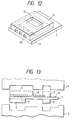
- Fig. 12 is a perspective view schematically showing a state where the solid layer is removed after the formation of the mold resin according to an embodiment of the present invention.
- Fig. 13 is cross-sectional view showing the structure of a recording head in a process where the energy generating elements, control signal input electrodes, and solid layer are formed.
- Figs. 14A and 14B are views showing the structure of the recording head in a process after the solid layer is removed.
- Fig. 14A is a cross-sectional view.
- Fig. 14B is a perspective view observed from the hollow hole side.
- Fig. 15 is a view illustrating the state where a recording head in a process is withdrawn from the formation die after the transfer mold formation.
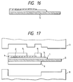
- Fig. 16 is a cross-sectional view schematically showing the state where the metal member and the substrate are coupled according to an embodiment of the present invention.
- Fig. 17 is a cross-sectional view schematically showing the state where the mold resin is formed by the application of the transfer formation and then, parted from the formation die.
- Fig. 18 is a cross-sectional view schematically showing an ink jet head when the solid layer is removed according to an embodiment of the present invention.
- Fig. 19 is a perspective view schematically showing an example of the head structure according to the present invention.
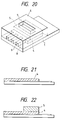
- Fig. 20 is a perspective view schematically showing a structural example of an ink jet head according to the present invention.
- Fig. 21 is a cross-sectional view schematically showing the state where a pattern for ink liquid passages and an ink liquid chamber is formed by a solid layer for the liquid passage formation according to an embodiment of the present invention.
- Fig. 22 is a cross-sectional view schematically showing the state where a solid layer for the formation of the liquid chamber is formed by a screen printing on the portion of a substrate where the formation of the ink liquid chamber is anticipated according to an embodiment of the present invention.
- Fig. 23 is a cross-sectional view schematically showing the state where a mold resin layer is formed by the application of transfer mold formation according to an embodiment of the present invention.
- Fig. 24 is a cross-sectional view schematically showing the completion of the functions as an ink jet head by removing the solid layer according to an embodiment of the present invention.
- Fig. 25 is a view illustrating an ink jet cartridge according to the present invention.
- Fig. 26 is a perspective view schematically illustrating a recording apparatus provided with an ink jet head according to the present invention.
- Fig. 27 is a graph showing the relationship between the mold thicknesses and the peeling frequency of the discharging ports.
- Fig. 1 is a perspective view schematically showing an example of an ink jet recording head according to a first embodiment of the present invention.
- Fig. 2 to Fig. 5 are schematic views illustrating the fundamental mode of a manufacture method according to the first embodiment of the present invention.
- Fig. 1 to Fig. 5 illustrate the structure of an ink jet recording head according to a manufacture method of the present invention, and an example of the process procedures thereof, respectively.
- an ink jet recording head having three discharging ports is illustrated, it is of course possible to equally manufacture a high density multi-array ink jet recording head which has its discharging ports in a number more than those illustrated.
- a substrate 1 made of a glass, ceramics, plastic, metal, or the like is used as shown in Fig. 2, for example.
- a substrate 1 such as this functions as a part of ink liquid passages, and is usable without any particular restrictions on its configuration, material, and others if only it is functional as a supporting member for a resist which will be described later.
- ink discharging energy generating elements 2 such as electrothermal transducers or piezoelectric elements are arranged in a desired number.
- the discharging energy to discharge ink droplets are provided by these ink discharging energy generating elements 2 for ink liquid for recording.
- the electrothermal transducers are used as the above-mentioned ink discharging energy generating elements 2
- the discharging energy is generated when these elements heat the ink in the vicinity thereof.
- the piezoelectric elements are used, for example, the discharging energy is generated by the mechanical vibration of these elements.
- control signal electrodes 3 are connected to these elements 2 for driving them. Also, in general, for the purpose of improving the durability of part of these discharging energy generating elements and the aforesaid electrodes, there are some cases where a protective film and various other functional layers are provided. There is no problem at all in providing such various functional layers in the present invention, too, as a matter of course.
- a solid layer 4 made of a resist, for example, which is dissolvable for removal by the application of a solvent or the like.
- the above-mentioned solid layer 4 comprises a solid layer 4a for the formation of an ink chamber and a solid layer 4b for the formation of the liquid passages as shown in Fig. 3B. Both the solid layers 4a and 4b are formed integrally.
- the solid layer 4 As a method for forming the solid layer 4, it is possible to employ among others a known method wherein a resist is laminated on the substrate 1, and then, the development is provided subsequent to the irradiation of light through a mask having the pattern for the solid layer.
- the resist those known of a positive or negative type can be utilized. Since the above-mentioned solid layer 4 is dissolved and removed in the latter process as described later, it is not necessarily limited to a resist. Various kinds of materials can be used if only such a material is removable.
- a mold resin layer 5 is formed to cover the solid layer 4 as shown in Fig. 4.
- the mold resin layer 5 is formed by the application of a transfer mold formation using a molding upper die 9 and molding lower die 10 capable of forming the contour of an ink jet recording head and an ink supply inlet 6 as shown in Fig. 4.
- the formation dies used for the transfer mold formation apparatus are arranged so that the portions of the formation dies corresponding to the ink discharging ports and ink liquid passages are structured to extrude more than the other portion in order to make the thickness X of the portions of the mold resin corresponding at least to the ink discarding port and ink liquid passages on the discharging port formation side thinner than the thickness Y of the other portion such as the liquid chamber formation part.
- the reason why the thickness of the resin is made thinner in such portion as above is to enable the later cutting process to be executed desirably only for the formation of the discharging ports.
- the thickness of the portions other than that of the discharging port formation should desirably be as thick as possible from the viewpoint of the structural strength.
- the methods other than the one used for the present embodiment are useable, such as an injection method using a liquid resin, injection formation, potting, and selective exposure method using the resin of an ultra-violet setting type.
- the transfer mold formation method is the best suited for the present invention.
- the material for the mold resin layer 5 there can be named an epoxy resin, allyl resin, diallylphthalate resin, silicon resin, polyester, phenol, and melamine.
- the materials which will be set at a normal temperature, or of a type such as heat setting and ultra violet setting among others can be used.
- acrylic resin, diglycol dialkyl carbonate resin, unsaturated polyester resin, polyurethane resin, polyimide resin, urea vesin can be named among others.
- the ink discharge characteristics vary in accordance with the length of the ink flow passage, it is possible to obtain the head by cutting the discharging port portion in a given position which is determined as an optimal position. Also, it may be possible to remove the solid layer after the discharging port portion is cut. In such a case, when the discarding port portion is cut the solid layer is still in the ink flow passages and others which will occupy the vital portion of the ink jet system. Thus, the clogging of the ink flow passages due to cut particles, dust particles, and the like and other related problems can be solved. Also, this is preferable because there is an advantage that in this way, the solid layer can be removed in a better condition.
- the thickness of the mold resin for the discharging port portion is made thinner than that of the other mold resin portions in order to relax the stress exerted in the mold resin for the portion where the preciseness is most demanded in an ink jet recording head.
- a cutting process is additionally required, but when a design consideration is made, there is an advantage in determining the initial thickness of the resin to be used because this contributes to defining the experimental conditions more freely rather than using the dies already established; hence making it possible to obtain more information required for a particular die designing.
- FIG. 6 to Figs. 9A and 9B are schematic views illustrating the fundamental mode of a manufacture method according to the present invention.
- the structure of an ink jet recording head according to the method of the present invention and an example of its manufacture procedures are represented.
- the present embodiment while an example of a mode using three discharging ports is shown, the present invention is not limited to this number as in the case of the first embodiment.
- a substrate 1 is prepared substantially in the same way as the first embodiment at first (Fig. 6).
- control signal input electrode 3 are connected to the elements 2 arranged on the substrate 1 to drive them.
- an Au, Al, Al - Cu - Si, Al - Si, and others can be used as the material for the aforesaid electrodes.
- the end portion of the control signal input electrodes opposite to the side where the discharging ports are arranged serves to function as an electrical junction (terminal) 12, and is connected to the recording apparatus main body by an electrical connecting member.
- the connection is executed by a bonding method using general aluminum wiring or the like. It is, therefore, necessary to prevent scratches, stains, resin flashes, and others from occurring in the aforesaid electrical junction 12.
- a first solid layer 4 with a pattern for the liquid passages and a liquid chamber formed thereon and a second layer 5 covering the aforesaid electrodes 3 at a given interval to the foregoing first solid layer are laminated.
- a resist and others can be used.
- a positive resist, AZ - 4000 series (Hexist Japan, Inc.), AZLP series (Hexist Japan, Inc.), PMEP - P - G7000 series (Tokyo Ohka, Inc.) or the like can be used.
- AZ - 4000 series Hexist Japan, Inc.
- AZLP series Hexist Japan, Inc.
- PMEP - P - G7000 series Tokyo Ohka, Inc.
- the formation of the solid layers on the substrate is made by a known photolithography or the like.
- Fig. 8 illustrates the state that a mold resin layer 6 is formed by the application of a transfer mold formation using a formation mold comprising an upper die 7 and a lower die 8 capable of forming the contour of an ink jet recording head and an ink supply inlet.
- a substrate 1 having the solid layers 4 and 5 formed thereon is inserted into either the upper die 7 or the lower die 8 provided with the arrangement of an appropriate liner, gate and air release. Then, the mold is closed.
- a heat setting epoxy resin as the material for the mold resin 6, the molding is performed in accordance with the general formation condition and process such as the resin preliminary heating at 60 to 90°C; injection pressure, 20 to 140 Kgf/cm2, formation die temperature, 100 to 180°C, pressurized setting time one to ten minutes, and a post curing after the formation.
- the formation characteristics (contour, air bubbles in the resin, burr, flash, and the like) should be ascertained and then, the respective points are defined appropriately.
- the higher the formation temperature the shorter is the setting time.
- the higher the injection pressure the smaller is the contour stability and the generation of air bubbles.
- any excessive pressure results in a damage to a produce and more problems of burr and flash of the resin.
- the timing of the post curing it is not necessarily executed in continuation with the formation. It may be possible to execute the curing at any point before the product is completely manufactured. Therefore, the post curing can be provided at any stage convenient to the process. It is of course possible to omit this process depending on the state in which the product will be used.
- a mold lubricant may be applied in some cases.
- the transfer mold method is the best suited for the present invention in consideration of its capability for a mass production, precision, and tact. It is of course possible to employ the other methods such as a potting method, a casting method using a liquid resin, an injection method, and a formation method by selective exposure using the resin of an ultraviolet radiation setting type. In any one of the formation methods, there is a need for a measure to prevent scratches, stains, burrs of the mold resin, or the like from occurring on the electrical junction by arranging the upper metallic die for the mold formation so that it is not in contact directly with the substrate.
- the method for removing the solid layer it is preferable to adopt a dissolution method wherein a recording head is immersed in an appropriate solvent so that the solid layer is dissolved and removed.
- the solvent it will suffice if only such a solvent does not destroy the mold resin layer. More specifically, if, for example, the solid layer is made of a positive resist, a caustic soda aqueous solution, and an organic solvent such as acetone or the like can be named. Further, in removal means, if the agitation of the solvent or promotion means such as the use of ultrasonic wave or the like is adopted together, it is possible to remove the solid layer more efficiently as a matter of course.
- the ink discharging characteristics vary in accordance with the length of the ink liquid passage
- the discharging port portion is cut in a desired ink liquid length by a known dicing method applicable to the wafer cutting subsequent to the adjustment of the length of the ink liquid passage in order to improve the ink discharging performance.
- the discarding port portion is cut, the solid layer is still in the ink flow passages and others which will occupy the vital portion of the ink jet system.
- the clogging of the ink flow passages due to cut particles, dust particles, and the like and other related problems can be solved.
- this is preferable because the length of the ink liquid passages is shortened when the solid layer is removed, and there is an advantage that the removal performance is improved among others.
- a substrate is prepared in the same manner as the foregoing embodiment.
- a solid layer 2 comprising a removable resist, dry film, or the like is formed.
- the resist the AZ - 4000 series (Hexist Japan, Inc.), AZLP series (Hexist Japan, Inc.) or the like can be used.
- This solid layer 2 is not necessarily limited to a resist if only the material used is removable.
- the formation of the energy generating elements and solid layer on the substrate is performed by a known photolithography or the like.
- a solid layer 3 which is also made of the same removable material is formed on the portion where the surface of the elements on the substrate 1, and the metallic die (in the example of the present embodiment, an upper die) used for the transfer mold formation, which will be described later, abut each other.
- Fig. 11 is a view schematically showing the state where a mold resin is formed by inserting a substrate 1 having the aforesaid solid layer formed thereon into the metallic mole (upper die and lower die) used for a transfer mold formation.
- the portion represented by slanted lines indicates the location of the solid layer 3 on the substrate 1 which is in contact with the upper die 4.
- the materials and method described in the foregoing embodiment are useable.
- the present invention demonstrates the effects on the protection of the substrate and the prevention of the defective formation (burrs and flashes of the non-mold part) by forming the solid layer made of material capable of removing the contact between the substrate and the resin or non-mold resin portion completely.
- the solid layers 2 and 3 are removed.
- a positive resist is used as the solid layer. Therefore, the solid layer can easily be removed by an aqueous solution containing 5 wt% caustic soda or an acetone or other organic solvent. Also, any solvent other than these ones is useable if only it has a selectivity (resistance to solvent) with respect to the mold resin. Further, in removal means, if an agitation of the solvent, ultrasonic wave, or other promoting means is added, the removal will be executed more efficiently as a matter of course.
- the ink flow length is cut in a desirable length by a known dicing method useable for cutting a wafer.
- Fig. 12 illustrates an ink jet recording head according to the present invention in which the solid layer is removed after the mold formation for the provision of the ink supply inlet 12, ink liquid passages 11 and ink discharging ports 10.
- a reference numeral 1 designates the substrate, and 9, the mold resin layer.
- a substrate 1 is prepared in the same manner as the foregoing embodiment.
- a solid layer 4 is formed by a resist which is removable by a solvent or the like, for example.
- the solid layer 4 is not necessarily mode of a resist. Any material can be used for the purpose if only such a material is removable by some means applicable.
- an outer frame 5 is formed by the application of a transfer mold formation.
- the means for removing the solid layer there is a method for dissolving it for removal by the use of a caustic soda aqueous solution or an acetone or some other organic solvent if the solid layer is made of a positive resist.
- the aforesaid solvent is not necessarily limited to those described above if only such a solvent does not destroy the outer frame formation material. Also, an agitation of the solvent, an ultrasonic wave, or some other promotional means is used together, the solid layer can be removed more efficiently as a matter of course.
- the ink discharging characteristics vary in accordance with the length of the ink passages. If required, therefore, the discharging port portion is obtained by cutting at a given position by determining an optimal position. The cutting is executed by a known dicing method or the like useable for a wafer cutting.
- Figs. 14A and 14B are views illustrating a process in which the substrate 1 and a metallic member 11 are coupled through the hollow hole 10 obtained by the aforesaid formation. In this way, the heat generated in the substrate 1 can be released to the metallic member 11.
- the metal material an Al, stainless, SiC, or the like can be named.
- the metallic member 11 is used to serve as a connecting part for the recording apparatus. It is also possible to mount the electrical components on the metallic member to drive the head.
- a substrate 1 is prepared in the same manner as the foregoing embodiment.
- a solid layer 4 is formed by a removable resist, for example, on the substrate 1 including the above-mentioned ink discharging energy generating elements 2.
- the method of forming the solid layer 4 it is possible to utilize a known method wherein a resist is laminated on the substrate 1, irradiated by light through a mask having the pattern of the solid layer, and developed.
- a known positive or negative one can be used for the resist.
- the above-mentioned solid layer 4 should be dissolved and removed in the latter process as described later. Therefore, the material is not necessarily limited to a resist, but any other material is useable if only such a material is removable.
- the substrate and a metallic member 5 is joined.
- a metal having a good heat radiation such as aluminum, SiC, SUS, or the like can be used.
- the electrical components such as ICs, flip chips, and others required to drive the head can be assembled.
- the aforesaid metallic member serves to function as a support to the substrate as well as a mounting member for the recording apparatus, and is bonded to the substrate by use of die bonding material, silver paste, silicon powder, UV adhesives, or various other adhesives.
- a mold resin layer 6 is formed by the application of a transfer mold formation.
- FIG. 18 is a perspective view illustrating this head.
- the recording head is immersed in an appropriate solvent to dissolve and remove the solid layer.
- an appropriate solvent it is preferable to apply a caustic soda aqueous solution or other alkali aqueous solution if the solid layer is made of a positive resist.
- an acetone or other organic solvent can be used.
- any other solvents than those mentioned above is applicable, if such a solvent has a selectivity (resistance to solvent) with respect to the mold resin. Further in removal means, if the agitation of the solvent, ultrasonic wave, or some other promoting means is used together, the removal can be executed more efficiently as a matter of course.
- the ink discharging characteristics vary in accordance with the length of the ink liquid passage. If required, therefore, it may be possible to adjust the length of the liquid passage in order to improve the ink discharging performance, and cut the discharging port portion in a desired length of the liquid passage by a known dicing method or the like usable as a method for cutting wafers.
- the present invention it is possible to remove the solid layer after the discharging port portion is cut.
- This method prevents cutting particles, dusts, and other from entering the ink liquid passages which occupy an important role in an ink jet recording head because when the discharging port portion is cut, the passages are filled with the solid layer.
- the solid layer is removed after the liquid passages, there is an advantage that the solid layer removal is performed in a better condition.
- Fig. 20 is a perspective view showing an ink jet recording head obtained by the present embodiment.
- a substrate 1 is prepared in the same manner as the foregoing embodiment.
- the method forming the solid layer 4 for the formation of the liquid passages it is possible to adopt a known method wherein a resist is laminated on the substrate 1, and developed after it is irradiated by light through a mask having the pattern for the solid layer.
- a known positive or negative one can be utilized as the resist.
- the above-mentioned solid layer 4 should be dissolved and removed in a latter process. Therefore, the material is not necessarily limited to a resist. Various other materials can be used if only such a material is removable.
- a solid layer 5 for the formation of a liquid chamber is provided on the portion on the substrate where the formation of a liquid chamber is anticipated.
- the material for the solid layer 5 for the formation of the liquid chamber it may be possible to adopt the same material as the one used for the solid layer 4 for the formation of the liquid passages or a different material. Further, the method for forming the solid layer 5 for the formation of the liquid chamber is the same as the one used for the solid layer 4 for the formation of the liquid passages. Moreover, it may be possible to form the solid layer 5 for the formation of the liquid chamber ahead of the formation of the liquid passages.
- the solid layer 5 for the formation of the liquid chamber two to ten times the thickness of the solid layer 4 for the formation of the liquid passages from the viewpoint of a desirable ink supply.
- a mold resin layer 6 is formed by the application of a transfer mold formation using the upper forming die 10 and a lower forming die 11 capable of forming the outer contour of a recording head and ink supply inlet.
- the method and material used for the transfer mold formation are the same as those applicable to the foregoing embodiment.
- a method wherein a recording head is immersed in an appropriate solvent to dissolve and remove the solid layers it is preferable to use a method wherein a recording head is immersed in an appropriate solvent to dissolve and remove the solid layers.
- the appropriate solvent it is preferable to use a caustic soda aqueous solution if the solid layers are made of a positive resist.
- acetone or other organic solvent is applicable.
- any other solvent other than those mentioned above can be used if only such a solvent does not destroy the mold resin.
- removal means it is possible to remove the solid layers more efficiently if the agitation of the solvent, ultrasonic wave, or other promoting means is employed together as a matter of course.
- the solid layer for the formation of the liquid passages and the solid layer for the formation of the liquid chamber are formed as an integrated solid layer, but these may be separate layers, or may be formed in the different processes.
- the present invention produces an excellent effect on ink jet recording methods, particularly a recording head and a recording apparatus wherein the flying droplets are formed by utilizing thermal energy in order to perform recording.
- the principle is such that at least one driving signal, which provides a rapid temperature rise beyond a departure from nucleation boiling point in response to recording information, is applied to an electrothermal transducer disposed on a liquid (ink) retaining sheet or liquid passage whereby to cause the electrothermal transducer to generate thermal energy to produce film boiling on the thermoactive portion of the recording head; thus effectively leading to the resultant formation of a bubble in the recording liquid (ink) one to one for each of the driving signals.
- the liquid (ink) is discharged through a discharging port to produce at least one droplet.
- the driving signal is preferably in the form of pulses because the development and contraction of the bubble can be effectuated instantaneously, and, therefore, the liquid (ink) is discharged with quick response.
- the driving signal in the form of pulses is preferably such as disclosed in the specifications of U.S. Patent Nos. 4,463,359 and 4,345,262.
- the temperature increasing rate of the heating surface is preferably such as disclosed in the specification of U.S. Patent No. 4,313,124 for an excellent recording in a better condition.
- the structure of the recording head may be as shown in each of the above-mentioned the specifications wherein the structure is arranged to combine the discharging ports, liquid passages, and the electrothermal transducers as disclosed in the above-mentioned patents (linear type liquid passage or right angle liquid passage).
- the structure such as disclosed in the specifications of U.S. Patent Nos. 4,558,333 and 4,459,600 wherein the thermal activation portions are arranged in a curved area is also included in the present invention.
- the present invention is applicable to the structure disclosed in Japanese Patent Laid-Open Application No. 59-123670 wherein a common slit is used as the discharging ports for plural electrothermal transducers, and to the structure disclosed in Japanese Patent Laid-Open Application No. 59-138461 wherein an opening for absorbing pressure wave of the thermal energy is formed corresponding to the discharging ports.
- the recording head for which the present invention is effectively utilized there is a recording head of a full-line type having a length corresponding to the maximum width of a recording medium recordable by a recording apparatus.
- This full-line head may be the one structured by combining a plurality of the recording heads disclosed in the above-mentioned specifications or a single full-line recording head which is integrally formed.
- the present invention is effectively applicable to a replaceable chip type recording head which is electrically connected with the main apparatus and for which the ink is supplied when it is mounted in the main assemble; or to a cartridge type recording head as shown in Fig. 25 having an ink tank 252 integrally provided for the recording head 251 itself.
- recording head recovery means and preliminarily auxiliary means additionally for a recording apparatus according to the present invention because these additional means will contribute to making the effectiveness of the present invention more stabilized.
- additional means are capping means for the recording head, cleaning means, compression or suction means, preliminary heating means such as electrothermal transducers or heating elements other than such transducers or the combination of those types of elements, and the preliminary discharge mode aside from the regular discharging for recording.
- the present invention is extremely effective in applying it not only a recording mode in which only main color such as black or the like, but also to an apparatus having at least one of a multi-color mode with ink of different colors, or a full-color mode using the mixture of the colors, irrespective of whether the recording head is integrally structured or it is structured by a combination of plural recording heads.
- the ink may be an ink material which is solidified below the room temperature but liquefied at the room temperature. Since the ink is controlled within the temperature not lower than 30°C and not higher than 70°C to stabilize its viscosity for the provision of the stable ejection in general, the ink may be such that it can be liquefied when the applicable recording signals are given.
- the most effective method for the respective ink mentioned above is the one which is capable of implementing the film boiling method described above.
- Fig. 26 is a perspective view showing the outer appearance of an example of the ink jet recording apparatus (IJRA) to which a liquid jet recording head obtainable by the present invention is bonded as an ink jet cartridge (IJC).
- IJRA ink jet recording apparatus
- IJC ink jet cartridge
- a reference numeral 20 designates an ink jet cartridge (IJC) provided with the nozzle group which discharges ink onto the recording surface of a recording sheet fed on a platen 24; and 16, a carriage HC holding the IJC 20, which is partly coupled to a driving belt 18 transmitting the driving force of a driving motor 17, and slidably mounted on the two guide shafts 19A and 19B arranged in parallel, thus enabling the IJC 20 to reciprocate along the entire width of the recording sheet.
- IJC ink jet cartridge
- a reference numeral 26 is a head recovery device which is arranged at one end of the traveling passage of the IJC 20, that is, a location opposite to its home position, for example.
- the head recovery device 26 is driven by the driving force of a motor 22 through a transmission mechanism 23 in order to cap the IJC 20.
- an ink suction is executed by an appropriate suction means provided in the head recovery device 26 or the pressurized ink feeding is actuated by an appropriate pressure means provided in the ink supply passage to the IJC 20.
- the ink is forcibly exhausted from the discharging ports to execute a discharge recovery process such as the removal of any overly viscous ink in the nozzles.
- the capping is performed to protect the IJC 20.
- a reference numeral 30 designates a wiping blade made of a silicon rubber, which is arranged at the side end of the head recovery device 26.
- the blade 30 is held by a blade holding member 30A in a cantilever fashion, and is driven by the motor 22 and the transmission mechanism 23 in the same manner as in the head recovery device 26; hence enabling it to engage with the discharging surface of the IJC 20.
- the blade 30 is allowed to extrude in the traveling passage of the IJC 20 at an appropriate timing during the recording operation of the IJC 20 or subsequent to the discharging recovery process using the head recovery device 26 in order to wire the dews, wets, or dust particles on the discharging surface of the IJC 20 along the traveling of the IJC 20.
- electrothermal transducers 2 (heaters made of HfB2) and electrodes 3 (made of Al) corresponding to the aforesaid electrothermal transducers 2 are formed in film by a deposition, sputtering, etching, or other semiconductor processing, and arranged at predetermined intervals so that the entire surface thereof becomes an element plane.
- a protective film and various other functional films are provided for the element plane including each of the electrodes 3 and electrothermal transducers 2, respectively, for the purpose of improving the durability.
- a positive resist is coated by a spinner coating in a given thickness. Then, using a mask pattern for ink liquid passages corresponding to the respective electrothermal transducers 2 and a liquid chamber, a solid layer 4 is formed through an exposure and a development process.
- the substrate 1 where the solid layer 4 is formed is molded by the application of a transfer mold formation.
- the substrate 1 where the solid layer 4 is formed is inserted into either an upper die or a lower die comprising a cavity provided with an appropriate runner, a gate, and an air escape arrangement. Then, the mold is closed.
- a heat setting epoxy resin is used as the material for the mold resin 5; hence making it possible to execute this process in accordance with a general formation condition and processing technique such as the resin preliminary heating temperature, 60 to 90°C, injection pressure, 20 to 140 kgf/cm2, formation temperature, 100 to 180°C, pressurized setting time, one to ten minutes, and then, a post curing.
- the preliminary heating temperature is set at 85°C
- the injection pressure 70 kgf/cm2
- formation temperature 150°C
- pressurized setting time four minutes.
- the resin used is a heat setting epoxy resin NT - 8506 (Nitto Inc.).
- the thickness of the mold resin for the discharging port portion and the ink flow passage portion which constitutes the point of the present invention, is set at 0.2 mm or more from the surface of the substrate 1, and a 1/2 or less of the thickness of the mold resin in the other portion in consideration of the mechanical strength and the relaxation of the stress of the mold resin. It is ascertained that this thickness arrangement demonstrates the best effect according to the experiment. Therefore, the molding dies are designed to obtain the aforesaid dimensions, and using them for the mold formation, the required configuration can be obtained all together at that time.
- the discharging port portion is cut by a known dicing method applicable to a wafer cutting in a given length of the ink flow passage, hence obtained a desired discharging port position.
- the solid layer 4 made of the aforesaid removable material is removed.
- a positive resist Product name: AZ - 4903 manufactured by Hexist Japan, Inc.
- a 5 wt% caustic soda aqueous solution, or acetone or other organic solvent can be used for the purpose.
- any others may be usable if only such a solvent has a selectivity with respect to the mold resin. In removing means, it is needless to mention that the removal can be executed more efficiently if the agitation of a solvent, ultrasonic wave, or other promoting means is used together.
- Fig. 27 there are shown the results of measurement given to the frequency with which the peeling of the discharging ports occurs by varying the ratio (X/Y) of the mold thicknesses.
- electrothermal transducers heads made of HfB2
- electrodes 3 made of Al
- film by a deposition, sputtering, etching, or other semiconductor processing, and arranged at predetermined intervals so that the entire surface thereof becomes an element plane.
- a protective film and various other functional films are provided for the element plane including each of the electrodes 3 and electrothermal transducers 2, respectively, for the purpose of improving the durability.
- a positive resist is coated by a spinner coating in a given thickness, and using a mask pattern for ink liquid passages corresponding to the respective electrothermal transducers 2 and a liquid chamber, a solid layer 4 is formed through an exposure and a development process as shown in Fig. 7.
- a solid layer 5 is formed in the same manner on the electrical junction on the substrate.
- the substrate 1 having the aforesaid solid layers 4 and 5 formed thereon is inserted into a transfer mold formation equipment to form a mold resin layer made of an epoxy resin.
- the formation condition is the preliminary heating is 80°C, preliminary heating injection pressure, 70 Kgf/cm2, formation temperature 150°C, and pressurized setting time, four minutes.
- the solid layers are dissolved and removed by a 5 wt% caustic soda aqueous solution to complete an ink jet recording head of the present invention.
- electrothermal transducers 2 (heaters made of HfB2) and electrodes 3 (made of Al) corresponding to the aforesaid electrothermal transducers 2 are formed in film by a deposition, sputtering, etching, or other semiconductor processing, and arranged at predetermined intervals so that the entire surface thereof becomes an element plane.
- a protective film and various other functional films are provided for the element plane including each of the electrodes 3 and electrothermal transducers 2, respectively, for the purpose of improving the durability.
- a positive resist is coated by a spinner coating in a given thickness, and using a mask pattern for ink liquid passages corresponding to the respective electrothermal transducers 2 and a liquid chamber, a solid layer 2 is formed through an exposure and a development process as shown in Fig. 11.
- the aforesaid mask pattern is arranged, and a solid layer 3 shown in Fig. 10 is also formed simultaneously.
- the substrate 1 having the aforesaid solid layers 2 and 3 formed thereon is inserted into a transfer mold formation equipment to form a mold resin layer made of an epoxy resin.
- the formation condition is the preliminary heating is 80°C, preliminary heating injection pressure, 70 Kgf/cm2, formation temperature 150°C, and pressurized setting time, four minutes.
- electrothermal transducers heads made of HfB2
- electrodes made of Al
- a protective film made of SiO2 is provided on the aforesaid element plane.
- a positive resist is spin coated in a thickness equal to the height of the ink discharging ports. Then, using a pattern mask for the ink passages corresponding to the respective electrothermal transducers, and an ink chamber, a solid layer 4 is formed through an exposure and development process.
- the outer frame which has a hollow hole is formed by the application of a transfer mold formation on condition of a preliminary heating at 80°C which uses a general microwave; injection pressure, 60 Kgf/cm2; formation temperature, 150°C; and pressurized setting time, four minutes.
- the aforesaid product in process is immersed in a 5 wt% caustic soda aqueous solution to dissolve and remove the solid layer made of a positive resist thereby to obtain the ink chamber, ink passages, and ink supply inlet.
- the substrate and a metallic member made of Al are adhesively bonded using a silicon compound (SH-340: Toray silicone, Inc., for example), thus obtaining an ink jet head of the present invention.
- a silicon compound SH-340: Toray silicone, Inc., for example
- electrothermal transducers 2 (heaters made of HfB2) and electrodes 3 (made of Al) corresponding to the aforesaid electrothermal transducers 2 are formed in film by a deposition, sputtering, etching, or other semiconductor processing, and arranged at predetermined intervals so that the entire surface thereof becomes an element plane.
- a protective film and various other functional films are provided for the element plane including each of the electrodes and electrothermal transducers, respectively, for the purpose of improving the durability.
- a positive resist is coated by a spinner coating in a given thickness, and using a mask pattern for ink liquid passages corresponding to the respective electrothermal transducers 2 and a liquid chamber, a solid layer 4 is formed through an exposure and a development process.
- the substrate 1 having the solid layer 4 formed thereon and a metallic member 5 are bonded in a given position.
- the substrate 1 bonded with the aforesaid metallic member 5 is inserted into a transfer mold formation apparatus to form a mold resin.
- the formation condition is: preliminary heating temperature, 80°C; injection pressure, 70 Kgf/cm2; formation temperature, 150°C; and pressurized setting time, four minutes.
- the solid layer 4 is removed.
- the layer is dissolve and removed by the application of a 5 wt% caustic soda aqueous solution.
- electrothermal transducers 2 (heaters made of HfB2) and electrodes 3 (made of Al) corresponding to the aforesaid electrothermal transducers 2 are formed in film by a deposition, sputtering, etching, or other semiconductor processing, and arranged at predetermined intervals so that the entire surface thereof becomes an element plane.
- a protective film and various other functional films are provided for the element plane including each of the electrodes 3 and electrothermal transducers 2, respectively, for the purpose of improving the durability.
- a positive resist is coated by a spinner coating in a given thickness, and using a mask pattern for ink liquid passages corresponding to the respective electrothermal transducers 2 and a liquid chamber, a solid layer 4 is formed through an exposure and a development process.
- a solid layer 5 for the formation of a liquid chamber is formed by the application of a printing method using a water soluble solder resist (Product name: Solder mask resist TC - 564 - S - SN: Sun-nopco, Inc.) in the present embodiment.
- the screen printing method is employed as means to form the solid layer 5, but the method is not limited thereto. If the method has means capable of executing the required formation without damaging the configuration of the solid layer 4, it may be possible to adopt a transfer method, stamp method, or the like without any problem, for example.
- the important point of the present invention is that at least the portion corresponding to the ink chamber is formed higher than that of the ink discharging port and ink liquid passage portions. This characterizes the present invention, and formation means to achieve this is not particularly limited.
- the formation condition is: using an epoxy resin as the mold resin, a preliminary heating in given at 80°C; formation temperature, 150°C; injection pressure, 70 Kgf/cm2; and pressurized setting time, 120 minutes.
- the discharging port portion is cut in a given length of the ink liquid passage by the application of a known dicing method usable for wafer cutting to obtain the discharging port surface.
- the solid layers 4 and 5 are dissolved and removed by the use of a 5 wt% caustic soda aqueous solution to obtain an ink jet head of the present invention.
- nega DF water soluble negative dry film
- the nega DF is again laminated to form a solid layer for the formation of the liquid chamber through exposure and development using a given pattern mask corresponding to the ink chamber.
- an ink jet recording head is manufactured in the same manner as the Embodiment 1.
Landscapes
- Engineering & Computer Science (AREA)
- Manufacturing & Machinery (AREA)
- Particle Formation And Scattering Control In Inkjet Printers (AREA)
Applications Claiming Priority (12)
| Application Number | Priority Date | Filing Date | Title |
|---|---|---|---|
| JP144503/92 | 1992-06-04 | ||
| JP14450392A JPH05330071A (ja) | 1992-06-04 | 1992-06-04 | インクジェット記録ヘッド、その製造方法、及びインクジェット記録ヘッドを備えた記録装置 |
| JP17119692A JP3004814B2 (ja) | 1992-06-29 | 1992-06-29 | インクジェット記録ヘッド、その製造方法及びインクジェット記録ヘッドを備えた記録装置 |
| JP171195/92 | 1992-06-29 | ||
| JP4171193A JP2997132B2 (ja) | 1992-06-29 | 1992-06-29 | インクジェット記録ヘッドの製造方法 |
| JP171196/92 | 1992-06-29 | ||
| JP171194/92 | 1992-06-29 | ||
| JP171197/92 | 1992-06-29 | ||
| JP17119492A JP3004812B2 (ja) | 1992-06-29 | 1992-06-29 | インクジェット記録ヘッド、その製造方法及びインクジェット記録ヘッドを備えた記録装置 |
| JP171193/92 | 1992-06-29 | ||
| JP17119592A JP3004813B2 (ja) | 1992-06-29 | 1992-06-29 | インクジェット記録ヘッド、その製造方法及びインクジェット記録ヘッドを備えた記録装置 |
| JP17119792A JP3093033B2 (ja) | 1992-06-29 | 1992-06-29 | インクジェット記録ヘッド、その製造方法及びインクジェット記録ヘッドを備えた記録装置 |
Publications (3)
| Publication Number | Publication Date |
|---|---|
| EP0573014A2 true EP0573014A2 (de) | 1993-12-08 |
| EP0573014A3 EP0573014A3 (en) | 1994-06-01 |
| EP0573014B1 EP0573014B1 (de) | 1998-10-28 |
Family
ID=27552985
Family Applications (1)
| Application Number | Title | Priority Date | Filing Date |
|---|---|---|---|
| EP93108875A Expired - Lifetime EP0573014B1 (de) | 1992-06-04 | 1993-06-02 | Tintenstrahlkopfherstellungsverfahren, nach dem Verfahren hergestellter Tintenstrahlkopf und Tintenstrahlgerät damit versehen |
Country Status (4)
| Country | Link |
|---|---|
| US (1) | US5774150A (de) |
| EP (1) | EP0573014B1 (de) |
| AT (1) | ATE172672T1 (de) |
| DE (1) | DE69321764T2 (de) |
Cited By (5)
| Publication number | Priority date | Publication date | Assignee | Title |
|---|---|---|---|---|
| EP0715957A3 (de) * | 1994-12-05 | 1996-11-20 | Canon Kk | Verfahren zur Herstellung eines Tintenstrahlkopfes |
| EP0749835A3 (de) * | 1995-06-20 | 1997-07-30 | Canon Kk | Verfahren zum Herstellen eines Tintenstrahlkopfes und Tintenstrahlkopf |
| EP0786347A3 (de) * | 1995-12-26 | 1997-09-10 | Canon Kk | |
| US5940957A (en) * | 1994-03-04 | 1999-08-24 | Canon Kabushiki Kaisha | Laser process for making a filter for an ink jet |
| AU2004201542B2 (en) * | 1995-06-20 | 2006-06-29 | Canon Kabushiki Kaisha | A Method for Manufacturing an Ink Jet Head, and an Ink Jet Head |
Families Citing this family (7)
| Publication number | Priority date | Publication date | Assignee | Title |
|---|---|---|---|---|
| JP3554159B2 (ja) * | 1996-11-12 | 2004-08-18 | キヤノン株式会社 | インクジェットヘッド及びインクジェットヘッドの製造方法 |
| JP3048957B2 (ja) * | 1997-05-26 | 2000-06-05 | 新潟日本電気株式会社 | 静電式インクジェットプリントヘッド |
| JP4731763B2 (ja) | 2001-09-12 | 2011-07-27 | キヤノン株式会社 | 液体噴射記録ヘッドおよびその製造方法 |
| US8018852B2 (en) * | 2003-08-22 | 2011-09-13 | Alcatel Lucent | Equal-cost source-resolved routing system and method |
| US7296871B2 (en) * | 2004-12-29 | 2007-11-20 | Lexmark International, Inc. | Device and structure arrangements for integrated circuits and methods for analyzing the same |
| JP4834426B2 (ja) * | 2006-03-06 | 2011-12-14 | キヤノン株式会社 | インクジェット記録ヘッドの製造方法 |
| AT521919B1 (de) * | 2018-12-13 | 2022-07-15 | Johann Kuebel Ing | Vorrichtung zur Abgabe von Licht |
Family Cites Families (16)
| Publication number | Priority date | Publication date | Assignee | Title |
|---|---|---|---|---|
| CA1127227A (en) * | 1977-10-03 | 1982-07-06 | Ichiro Endo | Liquid jet recording process and apparatus therefor |
| JPS54117205A (en) * | 1978-03-03 | 1979-09-12 | Canon Kk | Recording liquid |
| US4330787A (en) * | 1978-10-31 | 1982-05-18 | Canon Kabushiki Kaisha | Liquid jet recording device |
| US4345262A (en) * | 1979-02-19 | 1982-08-17 | Canon Kabushiki Kaisha | Ink jet recording method |
| US4463359A (en) * | 1979-04-02 | 1984-07-31 | Canon Kabushiki Kaisha | Droplet generating method and apparatus thereof |
| US4313124A (en) * | 1979-05-18 | 1982-01-26 | Canon Kabushiki Kaisha | Liquid jet recording process and liquid jet recording head |
| US4558333A (en) * | 1981-07-09 | 1985-12-10 | Canon Kabushiki Kaisha | Liquid jet recording head |
| JPS59123670A (ja) * | 1982-12-28 | 1984-07-17 | Canon Inc | インクジエツトヘツド |
| JPS59138461A (ja) * | 1983-01-28 | 1984-08-08 | Canon Inc | 液体噴射記録装置 |
| JPH0645242B2 (ja) * | 1984-12-28 | 1994-06-15 | キヤノン株式会社 | 液体噴射記録ヘツドの製造方法 |
| JPS62231761A (ja) * | 1985-11-06 | 1987-10-12 | Canon Inc | 液体噴射記録ヘツド |
| JPH0698755B2 (ja) * | 1986-04-28 | 1994-12-07 | キヤノン株式会社 | 液体噴射記録ヘツドの製造方法 |
| US4831390A (en) * | 1988-01-15 | 1989-05-16 | Xerox Corporation | Bubble jet printing device with improved printhead heat control |
| JPH01306251A (ja) * | 1988-06-03 | 1989-12-11 | Canon Inc | インクジェット記録ヘッド |
| US4878992A (en) * | 1988-11-25 | 1989-11-07 | Xerox Corporation | Method of fabricating thermal ink jet printheads |
| CA2048366C (en) * | 1990-08-03 | 1996-08-13 | Masatsune Kobayashi | Ink jet recording head molded member, apparatus comprising the same, and method of manufacturing the same |
-
1993
- 1993-06-02 AT AT93108875T patent/ATE172672T1/de active
- 1993-06-02 EP EP93108875A patent/EP0573014B1/de not_active Expired - Lifetime
- 1993-06-02 DE DE69321764T patent/DE69321764T2/de not_active Expired - Fee Related
-
1997
- 1997-01-03 US US08/778,283 patent/US5774150A/en not_active Expired - Lifetime
Cited By (9)
| Publication number | Priority date | Publication date | Assignee | Title |
|---|---|---|---|---|
| US5940957A (en) * | 1994-03-04 | 1999-08-24 | Canon Kabushiki Kaisha | Laser process for making a filter for an ink jet |
| USRE38710E1 (en) * | 1994-03-04 | 2005-03-15 | Canon Kabushiki Kaisha | Laser process for making a filter for an ink jet |
| EP0715957A3 (de) * | 1994-12-05 | 1996-11-20 | Canon Kk | Verfahren zur Herstellung eines Tintenstrahlkopfes |
| EP0749835A3 (de) * | 1995-06-20 | 1997-07-30 | Canon Kk | Verfahren zum Herstellen eines Tintenstrahlkopfes und Tintenstrahlkopf |
| US6145965A (en) * | 1995-06-20 | 2000-11-14 | Canon Kabushiki Kaisha | Method for manufacturing an ink jet head, and an ink jet head |
| CN1096952C (zh) * | 1995-06-20 | 2002-12-25 | 佳能株式会社 | 一种制造喷墨头的方法和一种喷墨头 |
| AU2004201542B2 (en) * | 1995-06-20 | 2006-06-29 | Canon Kabushiki Kaisha | A Method for Manufacturing an Ink Jet Head, and an Ink Jet Head |
| US6055729A (en) * | 1995-12-24 | 2000-05-02 | Canon Kabushiki Kaisha | Method for manufacturing a liquid jet recording head |
| EP0786347A3 (de) * | 1995-12-26 | 1997-09-10 | Canon Kk |
Also Published As
| Publication number | Publication date |
|---|---|
| DE69321764D1 (de) | 1998-12-03 |
| EP0573014A3 (en) | 1994-06-01 |
| ATE172672T1 (de) | 1998-11-15 |
| US5774150A (en) | 1998-06-30 |
| EP0573014B1 (de) | 1998-10-28 |
| DE69321764T2 (de) | 1999-05-06 |
Similar Documents
| Publication | Publication Date | Title |
|---|---|---|
| JP3592172B2 (ja) | インクジェット記録ヘッドの製造方法、該製法によって製造されたインクジェット記録ヘッド及び該インクジェット記録ヘッドを搭載したインクジェット記録装置 | |
| US6449831B1 (en) | Process for making a heater chip module | |
| US5774150A (en) | Method for manufacturing ink jet head, ink jet head manufactured by such a method, and ink jet apparatus provided with such a head | |
| US6039439A (en) | Ink jet heater chip module | |
| EP1162068B1 (de) | Verfahren zum Herstellen eines Flüssigkeitsstrahlaufzeichnungskopfes | |
| JP3861532B2 (ja) | インクジェットプリンタヘッドの製造方法 | |
| JPH091812A (ja) | 液体噴射記録ヘッドの製造方法および製造装置 | |
| JP2997132B2 (ja) | インクジェット記録ヘッドの製造方法 | |
| JP3093033B2 (ja) | インクジェット記録ヘッド、その製造方法及びインクジェット記録ヘッドを備えた記録装置 | |
| US6582053B1 (en) | Method for manufacturing a liquid jet recording head and a liquid jet recording head manufactured by such method | |
| JP3004814B2 (ja) | インクジェット記録ヘッド、その製造方法及びインクジェット記録ヘッドを備えた記録装置 | |
| JP3004813B2 (ja) | インクジェット記録ヘッド、その製造方法及びインクジェット記録ヘッドを備えた記録装置 | |
| JPH08142327A (ja) | インクジェット記録装置の記録ヘッド | |
| JP3004812B2 (ja) | インクジェット記録ヘッド、その製造方法及びインクジェット記録ヘッドを備えた記録装置 | |
| JPH07164639A (ja) | インクジェット記録ヘッド、その製造方法、およびその記録ヘッドを備えた記録装置 | |
| JPH07156414A (ja) | インクジェット記録ヘッドの製造方法、インクジェット記録ヘッド、および記録装置 | |
| JP2959602B2 (ja) | インクジェット記録ヘッド、その製造方法、該記録ヘッドを備えた記録装置及びインクジェット記録ヘッドに用いるトランスファーモールド用エポキシ樹脂組成物 | |
| JP3107876B2 (ja) | インクジェット記録ヘッドの製造方法、該製造方法で製造したインクジェット記録ヘッドおよび該記録ヘッドを備えた記録装置 | |
| JPH09277539A (ja) | インクジェットプリントヘッド、その製造方法およびインクジェットプリント装置 | |
| JPH10114070A (ja) | 液体噴射記録ヘッドおよびその製造方法 | |
| JP3311023B2 (ja) | インクジェット記録ヘッドの製造方法 | |
| JPH068455A (ja) | インクジェット記録ヘッド、その製造方法及び該記録ヘッドを備えた記録装置 | |
| JP2004058287A (ja) | 液体吐出ヘッド | |
| JPH05162319A (ja) | インクジェット記録ヘッド、その製造方法及び該ヘッドを備えたインクジェット記録装置 | |
| JPH091810A (ja) | インクジェット記録ヘッドの製造方法、該製造方法により製造される記録ヘッド及び該記録ヘッドを備えた記録装置 |
Legal Events
| Date | Code | Title | Description |
|---|---|---|---|
| PUAI | Public reference made under article 153(3) epc to a published international application that has entered the european phase |
Free format text: ORIGINAL CODE: 0009012 |
|
| AK | Designated contracting states |
Kind code of ref document: A2 Designated state(s): AT BE CH DE DK ES FR GB GR IE IT LI LU NL PT SE |
|
| PUAL | Search report despatched |
Free format text: ORIGINAL CODE: 0009013 |
|
| AK | Designated contracting states |
Kind code of ref document: A3 Designated state(s): AT BE CH DE DK ES FR GB GR IE IT LI LU NL PT SE |
|
| 17P | Request for examination filed |
Effective date: 19941018 |
|
| 17Q | First examination report despatched |
Effective date: 19950908 |
|
| GRAG | Despatch of communication of intention to grant |
Free format text: ORIGINAL CODE: EPIDOS AGRA |
|
| GRAG | Despatch of communication of intention to grant |
Free format text: ORIGINAL CODE: EPIDOS AGRA |
|
| GRAH | Despatch of communication of intention to grant a patent |
Free format text: ORIGINAL CODE: EPIDOS IGRA |
|
| GRAH | Despatch of communication of intention to grant a patent |
Free format text: ORIGINAL CODE: EPIDOS IGRA |
|
| GRAA | (expected) grant |
Free format text: ORIGINAL CODE: 0009210 |
|
| AK | Designated contracting states |
Kind code of ref document: B1 Designated state(s): AT BE CH DE DK ES FR GB GR IE IT LI LU NL PT SE |
|
| PG25 | Lapsed in a contracting state [announced via postgrant information from national office to epo] |
Ref country code: NL Free format text: LAPSE BECAUSE OF FAILURE TO SUBMIT A TRANSLATION OF THE DESCRIPTION OR TO PAY THE FEE WITHIN THE PRESCRIBED TIME-LIMIT Effective date: 19981028 Ref country code: LI Free format text: LAPSE BECAUSE OF FAILURE TO SUBMIT A TRANSLATION OF THE DESCRIPTION OR TO PAY THE FEE WITHIN THE PRESCRIBED TIME-LIMIT Effective date: 19981028 Ref country code: GR Free format text: LAPSE BECAUSE OF NON-PAYMENT OF DUE FEES Effective date: 19981028 Ref country code: ES Free format text: THE PATENT HAS BEEN ANNULLED BY A DECISION OF A NATIONAL AUTHORITY Effective date: 19981028 Ref country code: CH Free format text: LAPSE BECAUSE OF FAILURE TO SUBMIT A TRANSLATION OF THE DESCRIPTION OR TO PAY THE FEE WITHIN THE PRESCRIBED TIME-LIMIT Effective date: 19981028 Ref country code: BE Free format text: LAPSE BECAUSE OF FAILURE TO SUBMIT A TRANSLATION OF THE DESCRIPTION OR TO PAY THE FEE WITHIN THE PRESCRIBED TIME-LIMIT Effective date: 19981028 Ref country code: AT Free format text: LAPSE BECAUSE OF FAILURE TO SUBMIT A TRANSLATION OF THE DESCRIPTION OR TO PAY THE FEE WITHIN THE PRESCRIBED TIME-LIMIT Effective date: 19981028 |
|
| REF | Corresponds to: |
Ref document number: 172672 Country of ref document: AT Date of ref document: 19981115 Kind code of ref document: T |
|
| REG | Reference to a national code |
Ref country code: CH Ref legal event code: EP |
|
| REF | Corresponds to: |
Ref document number: 69321764 Country of ref document: DE Date of ref document: 19981203 |
|
| REG | Reference to a national code |
Ref country code: IE Ref legal event code: FG4D |
|
| PG25 | Lapsed in a contracting state [announced via postgrant information from national office to epo] |
Ref country code: SE Free format text: LAPSE BECAUSE OF FAILURE TO SUBMIT A TRANSLATION OF THE DESCRIPTION OR TO PAY THE FEE WITHIN THE PRESCRIBED TIME-LIMIT Effective date: 19990128 Ref country code: PT Free format text: LAPSE BECAUSE OF FAILURE TO SUBMIT A TRANSLATION OF THE DESCRIPTION OR TO PAY THE FEE WITHIN THE PRESCRIBED TIME-LIMIT Effective date: 19990128 Ref country code: DK Free format text: LAPSE BECAUSE OF FAILURE TO SUBMIT A TRANSLATION OF THE DESCRIPTION OR TO PAY THE FEE WITHIN THE PRESCRIBED TIME-LIMIT Effective date: 19990128 |
|
| ET | Fr: translation filed | ||
| NLV1 | Nl: lapsed or annulled due to failure to fulfill the requirements of art. 29p and 29m of the patents act | ||
| REG | Reference to a national code |
Ref country code: CH Ref legal event code: PL |
|
| PG25 | Lapsed in a contracting state [announced via postgrant information from national office to epo] |
Ref country code: LU Free format text: LAPSE BECAUSE OF NON-PAYMENT OF DUE FEES Effective date: 19990602 Ref country code: IE Free format text: LAPSE BECAUSE OF NON-PAYMENT OF DUE FEES Effective date: 19990602 |
|
| PLBE | No opposition filed within time limit |
Free format text: ORIGINAL CODE: 0009261 |
|
| STAA | Information on the status of an ep patent application or granted ep patent |
Free format text: STATUS: NO OPPOSITION FILED WITHIN TIME LIMIT |
|
| 26N | No opposition filed | ||
| REG | Reference to a national code |
Ref country code: IE Ref legal event code: MM4A |
|
| REG | Reference to a national code |
Ref country code: GB Ref legal event code: IF02 |
|
| PGFP | Annual fee paid to national office [announced via postgrant information from national office to epo] |
Ref country code: IT Payment date: 20090622 Year of fee payment: 17 |
|
| PGFP | Annual fee paid to national office [announced via postgrant information from national office to epo] |
Ref country code: GB Payment date: 20090626 Year of fee payment: 17 Ref country code: DE Payment date: 20090630 Year of fee payment: 17 |
|
| GBPC | Gb: european patent ceased through non-payment of renewal fee |
Effective date: 20100602 |
|
| REG | Reference to a national code |
Ref country code: FR Ref legal event code: ST Effective date: 20110228 |
|
| PG25 | Lapsed in a contracting state [announced via postgrant information from national office to epo] |
Ref country code: IT Free format text: LAPSE BECAUSE OF NON-PAYMENT OF DUE FEES Effective date: 20100602 |
|
| PG25 | Lapsed in a contracting state [announced via postgrant information from national office to epo] |
Ref country code: DE Free format text: LAPSE BECAUSE OF NON-PAYMENT OF DUE FEES Effective date: 20110101 |
|
| PG25 | Lapsed in a contracting state [announced via postgrant information from national office to epo] |
Ref country code: FR Free format text: LAPSE BECAUSE OF NON-PAYMENT OF DUE FEES Effective date: 20100630 |
|
| PG25 | Lapsed in a contracting state [announced via postgrant information from national office to epo] |
Ref country code: GB Free format text: LAPSE BECAUSE OF NON-PAYMENT OF DUE FEES Effective date: 20100602 |
|
| PGFP | Annual fee paid to national office [announced via postgrant information from national office to epo] |
Ref country code: FR Payment date: 20090624 Year of fee payment: 17 |