EP0572231A2 - Tintenstrahldruckkopf - Google Patents
Tintenstrahldruckkopf Download PDFInfo
- Publication number
- EP0572231A2 EP0572231A2 EP93304070A EP93304070A EP0572231A2 EP 0572231 A2 EP0572231 A2 EP 0572231A2 EP 93304070 A EP93304070 A EP 93304070A EP 93304070 A EP93304070 A EP 93304070A EP 0572231 A2 EP0572231 A2 EP 0572231A2
- Authority
- EP
- European Patent Office
- Prior art keywords
- ink
- plate
- print head
- piezoelectric
- pump member
- Prior art date
- Legal status (The legal status is an assumption and is not a legal conclusion. Google has not performed a legal analysis and makes no representation as to the accuracy of the status listed.)
- Granted
Links
- 238000004891 communication Methods 0.000 claims abstract description 29
- 125000006850 spacer group Chemical group 0.000 claims abstract description 21
- 238000000034 method Methods 0.000 claims abstract description 17
- 239000000919 ceramic Substances 0.000 claims abstract description 16
- 230000008859 change Effects 0.000 claims abstract description 4
- MCMNRKCIXSYSNV-UHFFFAOYSA-N Zirconium dioxide Chemical compound O=[Zr]=O MCMNRKCIXSYSNV-UHFFFAOYSA-N 0.000 claims description 18
- 229910010293 ceramic material Inorganic materials 0.000 claims description 4
- 238000007650 screen-printing Methods 0.000 claims description 4
- 239000011248 coating agent Substances 0.000 claims description 3
- 238000000576 coating method Methods 0.000 claims description 3
- PNEYBMLMFCGWSK-UHFFFAOYSA-N aluminium oxide Inorganic materials [O-2].[O-2].[O-2].[Al+3].[Al+3] PNEYBMLMFCGWSK-UHFFFAOYSA-N 0.000 claims description 2
- 238000007598 dipping method Methods 0.000 claims description 2
- 239000010419 fine particle Substances 0.000 claims description 2
- 238000007733 ion plating Methods 0.000 claims description 2
- 238000010884 ion-beam technique Methods 0.000 claims description 2
- 229910002077 partially stabilized zirconia Inorganic materials 0.000 claims description 2
- 238000007747 plating Methods 0.000 claims description 2
- 238000005507 spraying Methods 0.000 claims description 2
- 238000004544 sputter deposition Methods 0.000 claims description 2
- 238000007740 vapor deposition Methods 0.000 claims description 2
- 229910002078 fully stabilized zirconia Inorganic materials 0.000 claims 1
- 239000000853 adhesive Substances 0.000 description 23
- 230000001070 adhesive effect Effects 0.000 description 23
- 239000000463 material Substances 0.000 description 21
- 239000010408 film Substances 0.000 description 9
- 150000001875 compounds Chemical class 0.000 description 6
- 238000007641 inkjet printing Methods 0.000 description 6
- 238000004519 manufacturing process Methods 0.000 description 6
- 230000002829 reductive effect Effects 0.000 description 6
- 239000000758 substrate Substances 0.000 description 6
- 239000013078 crystal Substances 0.000 description 5
- 229910052751 metal Inorganic materials 0.000 description 5
- 239000002184 metal Substances 0.000 description 5
- PXHVJJICTQNCMI-UHFFFAOYSA-N Nickel Chemical compound [Ni] PXHVJJICTQNCMI-UHFFFAOYSA-N 0.000 description 4
- 238000006073 displacement reaction Methods 0.000 description 4
- SIWVEOZUMHYXCS-UHFFFAOYSA-N oxo(oxoyttriooxy)yttrium Chemical compound O=[Y]O[Y]=O SIWVEOZUMHYXCS-UHFFFAOYSA-N 0.000 description 4
- 230000008569 process Effects 0.000 description 4
- 229910045601 alloy Inorganic materials 0.000 description 3
- 239000000956 alloy Substances 0.000 description 3
- RKTYLMNFRDHKIL-UHFFFAOYSA-N copper;5,10,15,20-tetraphenylporphyrin-22,24-diide Chemical compound [Cu+2].C1=CC(C(=C2C=CC([N-]2)=C(C=2C=CC=CC=2)C=2C=CC(N=2)=C(C=2C=CC=CC=2)C2=CC=C3[N-]2)C=2C=CC=CC=2)=NC1=C3C1=CC=CC=C1 RKTYLMNFRDHKIL-UHFFFAOYSA-N 0.000 description 3
- 230000000694 effects Effects 0.000 description 3
- 238000010304 firing Methods 0.000 description 3
- 239000002245 particle Substances 0.000 description 3
- 238000004080 punching Methods 0.000 description 3
- 230000002441 reversible effect Effects 0.000 description 3
- 238000007789 sealing Methods 0.000 description 3
- YLQBMQCUIZJEEH-UHFFFAOYSA-N Furan Chemical compound C=1C=COC=1 YLQBMQCUIZJEEH-UHFFFAOYSA-N 0.000 description 2
- XEEYBQQBJWHFJM-UHFFFAOYSA-N Iron Chemical compound [Fe] XEEYBQQBJWHFJM-UHFFFAOYSA-N 0.000 description 2
- KDLHZDBZIXYQEI-UHFFFAOYSA-N Palladium Chemical compound [Pd] KDLHZDBZIXYQEI-UHFFFAOYSA-N 0.000 description 2
- 229910001252 Pd alloy Inorganic materials 0.000 description 2
- 229910052787 antimony Inorganic materials 0.000 description 2
- 230000015572 biosynthetic process Effects 0.000 description 2
- -1 cadnium Chemical compound 0.000 description 2
- BRPQOXSCLDDYGP-UHFFFAOYSA-N calcium oxide Chemical compound [O-2].[Ca+2] BRPQOXSCLDDYGP-UHFFFAOYSA-N 0.000 description 2
- 239000000292 calcium oxide Substances 0.000 description 2
- ODINCKMPIJJUCX-UHFFFAOYSA-N calcium oxide Inorganic materials [Ca]=O ODINCKMPIJJUCX-UHFFFAOYSA-N 0.000 description 2
- 229910000420 cerium oxide Inorganic materials 0.000 description 2
- 238000010438 heat treatment Methods 0.000 description 2
- 239000012943 hotmelt Substances 0.000 description 2
- 238000003475 lamination Methods 0.000 description 2
- 229910052451 lead zirconate titanate Inorganic materials 0.000 description 2
- 238000003754 machining Methods 0.000 description 2
- 239000000395 magnesium oxide Substances 0.000 description 2
- CPLXHLVBOLITMK-UHFFFAOYSA-N magnesium oxide Inorganic materials [Mg]=O CPLXHLVBOLITMK-UHFFFAOYSA-N 0.000 description 2
- AXZKOIWUVFPNLO-UHFFFAOYSA-N magnesium;oxygen(2-) Chemical compound [O-2].[Mg+2] AXZKOIWUVFPNLO-UHFFFAOYSA-N 0.000 description 2
- 239000000203 mixture Substances 0.000 description 2
- 229910052759 nickel Inorganic materials 0.000 description 2
- BMMGVYCKOGBVEV-UHFFFAOYSA-N oxo(oxoceriooxy)cerium Chemical compound [Ce]=O.O=[Ce]=O BMMGVYCKOGBVEV-UHFFFAOYSA-N 0.000 description 2
- 238000005192 partition Methods 0.000 description 2
- BASFCYQUMIYNBI-UHFFFAOYSA-N platinum Chemical compound [Pt] BASFCYQUMIYNBI-UHFFFAOYSA-N 0.000 description 2
- 230000010287 polarization Effects 0.000 description 2
- 229920000728 polyester Polymers 0.000 description 2
- 229920000098 polyolefin Polymers 0.000 description 2
- 239000002243 precursor Substances 0.000 description 2
- GHMLBKRAJCXXBS-UHFFFAOYSA-N resorcinol Chemical compound OC1=CC=CC(O)=C1 GHMLBKRAJCXXBS-UHFFFAOYSA-N 0.000 description 2
- 239000000057 synthetic resin Substances 0.000 description 2
- 229920003002 synthetic resin Polymers 0.000 description 2
- 229910052684 Cerium Inorganic materials 0.000 description 1
- VYZAMTAEIAYCRO-UHFFFAOYSA-N Chromium Chemical compound [Cr] VYZAMTAEIAYCRO-UHFFFAOYSA-N 0.000 description 1
- 239000004593 Epoxy Substances 0.000 description 1
- PWHULOQIROXLJO-UHFFFAOYSA-N Manganese Chemical compound [Mn] PWHULOQIROXLJO-UHFFFAOYSA-N 0.000 description 1
- 229920000877 Melamine resin Polymers 0.000 description 1
- ISWSIDIOOBJBQZ-UHFFFAOYSA-N Phenol Chemical compound OC1=CC=CC=C1 ISWSIDIOOBJBQZ-UHFFFAOYSA-N 0.000 description 1
- 239000004952 Polyamide Substances 0.000 description 1
- 239000004642 Polyimide Substances 0.000 description 1
- 229910001260 Pt alloy Inorganic materials 0.000 description 1
- XSQUKJJJFZCRTK-UHFFFAOYSA-N Urea Chemical compound NC(N)=O XSQUKJJJFZCRTK-UHFFFAOYSA-N 0.000 description 1
- HCHKCACWOHOZIP-UHFFFAOYSA-N Zinc Chemical compound [Zn] HCHKCACWOHOZIP-UHFFFAOYSA-N 0.000 description 1
- IHWJXGQYRBHUIF-UHFFFAOYSA-N [Ag].[Pt] Chemical compound [Ag].[Pt] IHWJXGQYRBHUIF-UHFFFAOYSA-N 0.000 description 1
- 230000002159 abnormal effect Effects 0.000 description 1
- 239000000654 additive Substances 0.000 description 1
- 230000000996 additive effect Effects 0.000 description 1
- WATWJIUSRGPENY-UHFFFAOYSA-N antimony atom Chemical compound [Sb] WATWJIUSRGPENY-UHFFFAOYSA-N 0.000 description 1
- 229910052788 barium Inorganic materials 0.000 description 1
- DSAJWYNOEDNPEQ-UHFFFAOYSA-N barium atom Chemical compound [Ba] DSAJWYNOEDNPEQ-UHFFFAOYSA-N 0.000 description 1
- 239000011230 binding agent Substances 0.000 description 1
- 239000004202 carbamide Substances 0.000 description 1
- ZMIGMASIKSOYAM-UHFFFAOYSA-N cerium Chemical compound [Ce][Ce][Ce][Ce][Ce][Ce][Ce][Ce][Ce][Ce][Ce][Ce][Ce][Ce][Ce][Ce][Ce][Ce][Ce][Ce][Ce][Ce][Ce][Ce][Ce][Ce][Ce][Ce][Ce][Ce][Ce][Ce][Ce][Ce][Ce][Ce][Ce][Ce] ZMIGMASIKSOYAM-UHFFFAOYSA-N 0.000 description 1
- 229910052804 chromium Inorganic materials 0.000 description 1
- 239000011651 chromium Substances 0.000 description 1
- 229910017052 cobalt Inorganic materials 0.000 description 1
- 239000010941 cobalt Substances 0.000 description 1
- GUTLYIVDDKVIGB-UHFFFAOYSA-N cobalt atom Chemical compound [Co] GUTLYIVDDKVIGB-UHFFFAOYSA-N 0.000 description 1
- 239000004020 conductor Substances 0.000 description 1
- 238000010276 construction Methods 0.000 description 1
- 239000002178 crystalline material Substances 0.000 description 1
- 238000005520 cutting process Methods 0.000 description 1
- 230000002950 deficient Effects 0.000 description 1
- NKZSPGSOXYXWQA-UHFFFAOYSA-N dioxido(oxo)titanium;lead(2+) Chemical compound [Pb+2].[O-][Ti]([O-])=O NKZSPGSOXYXWQA-UHFFFAOYSA-N 0.000 description 1
- 229920001971 elastomer Polymers 0.000 description 1
- 239000007772 electrode material Substances 0.000 description 1
- 229920006332 epoxy adhesive Polymers 0.000 description 1
- 239000000945 filler Substances 0.000 description 1
- 239000011521 glass Substances 0.000 description 1
- 238000000227 grinding Methods 0.000 description 1
- 230000002401 inhibitory effect Effects 0.000 description 1
- 238000001746 injection moulding Methods 0.000 description 1
- 238000009413 insulation Methods 0.000 description 1
- 229910052742 iron Inorganic materials 0.000 description 1
- 229910052746 lanthanum Inorganic materials 0.000 description 1
- FZLIPJUXYLNCLC-UHFFFAOYSA-N lanthanum atom Chemical compound [La] FZLIPJUXYLNCLC-UHFFFAOYSA-N 0.000 description 1
- HEPLMSKRHVKCAQ-UHFFFAOYSA-N lead nickel Chemical compound [Ni].[Pb] HEPLMSKRHVKCAQ-UHFFFAOYSA-N 0.000 description 1
- JQJCSZOEVBFDKO-UHFFFAOYSA-N lead zinc Chemical compound [Zn].[Pb] JQJCSZOEVBFDKO-UHFFFAOYSA-N 0.000 description 1
- HFGPZNIAWCZYJU-UHFFFAOYSA-N lead zirconate titanate Chemical compound [O-2].[O-2].[O-2].[O-2].[O-2].[Ti+4].[Zr+4].[Pb+2] HFGPZNIAWCZYJU-UHFFFAOYSA-N 0.000 description 1
- 239000007788 liquid Substances 0.000 description 1
- 229910052748 manganese Inorganic materials 0.000 description 1
- 239000011572 manganese Substances 0.000 description 1
- WPBNNNQJVZRUHP-UHFFFAOYSA-L manganese(2+);methyl n-[[2-(methoxycarbonylcarbamothioylamino)phenyl]carbamothioyl]carbamate;n-[2-(sulfidocarbothioylamino)ethyl]carbamodithioate Chemical compound [Mn+2].[S-]C(=S)NCCNC([S-])=S.COC(=O)NC(=S)NC1=CC=CC=C1NC(=S)NC(=O)OC WPBNNNQJVZRUHP-UHFFFAOYSA-L 0.000 description 1
- JDSHMPZPIAZGSV-UHFFFAOYSA-N melamine Chemical compound NC1=NC(N)=NC(N)=N1 JDSHMPZPIAZGSV-UHFFFAOYSA-N 0.000 description 1
- 238000002844 melting Methods 0.000 description 1
- 230000008018 melting Effects 0.000 description 1
- 150000002739 metals Chemical class 0.000 description 1
- 238000002156 mixing Methods 0.000 description 1
- 230000004048 modification Effects 0.000 description 1
- 238000012986 modification Methods 0.000 description 1
- 238000000465 moulding Methods 0.000 description 1
- 229910052758 niobium Inorganic materials 0.000 description 1
- 239000010955 niobium Substances 0.000 description 1
- GUCVJGMIXFAOAE-UHFFFAOYSA-N niobium atom Chemical compound [Nb] GUCVJGMIXFAOAE-UHFFFAOYSA-N 0.000 description 1
- 229910000510 noble metal Inorganic materials 0.000 description 1
- 230000001590 oxidative effect Effects 0.000 description 1
- ZBSCCQXBYNSKPV-UHFFFAOYSA-N oxolead;oxomagnesium;2,4,5-trioxa-1$l^{5},3$l^{5}-diniobabicyclo[1.1.1]pentane 1,3-dioxide Chemical compound [Mg]=O.[Pb]=O.[Pb]=O.[Pb]=O.O1[Nb]2(=O)O[Nb]1(=O)O2 ZBSCCQXBYNSKPV-UHFFFAOYSA-N 0.000 description 1
- 229910052763 palladium Inorganic materials 0.000 description 1
- SWELZOZIOHGSPA-UHFFFAOYSA-N palladium silver Chemical compound [Pd].[Ag] SWELZOZIOHGSPA-UHFFFAOYSA-N 0.000 description 1
- 230000036961 partial effect Effects 0.000 description 1
- 239000004033 plastic Substances 0.000 description 1
- 229920003023 plastic Polymers 0.000 description 1
- 229910052697 platinum Inorganic materials 0.000 description 1
- 229920002647 polyamide Polymers 0.000 description 1
- 229920001721 polyimide Polymers 0.000 description 1
- 229920001296 polysiloxane Polymers 0.000 description 1
- 229920002635 polyurethane Polymers 0.000 description 1
- 239000004814 polyurethane Substances 0.000 description 1
- 238000007639 printing Methods 0.000 description 1
- 230000009467 reduction Effects 0.000 description 1
- 229920005989 resin Polymers 0.000 description 1
- 239000011347 resin Substances 0.000 description 1
- 230000004044 response Effects 0.000 description 1
- 229910052703 rhodium Inorganic materials 0.000 description 1
- 239000010948 rhodium Substances 0.000 description 1
- MHOVAHRLVXNVSD-UHFFFAOYSA-N rhodium atom Chemical compound [Rh] MHOVAHRLVXNVSD-UHFFFAOYSA-N 0.000 description 1
- 239000004065 semiconductor Substances 0.000 description 1
- 239000002002 slurry Substances 0.000 description 1
- 239000002904 solvent Substances 0.000 description 1
- 229910002076 stabilized zirconia Inorganic materials 0.000 description 1
- 230000000087 stabilizing effect Effects 0.000 description 1
- 239000010935 stainless steel Substances 0.000 description 1
- 229910001220 stainless steel Inorganic materials 0.000 description 1
- 229940071182 stannate Drugs 0.000 description 1
- 229910052712 strontium Inorganic materials 0.000 description 1
- CIOAGBVUUVVLOB-UHFFFAOYSA-N strontium atom Chemical compound [Sr] CIOAGBVUUVVLOB-UHFFFAOYSA-N 0.000 description 1
- 229910052715 tantalum Inorganic materials 0.000 description 1
- GUVRBAGPIYLISA-UHFFFAOYSA-N tantalum atom Chemical compound [Ta] GUVRBAGPIYLISA-UHFFFAOYSA-N 0.000 description 1
- 239000010409 thin film Substances 0.000 description 1
- 230000009466 transformation Effects 0.000 description 1
- 238000000844 transformation Methods 0.000 description 1
- WFKWXMTUELFFGS-UHFFFAOYSA-N tungsten Chemical compound [W] WFKWXMTUELFFGS-UHFFFAOYSA-N 0.000 description 1
- 229910052721 tungsten Inorganic materials 0.000 description 1
- 239000010937 tungsten Substances 0.000 description 1
- 125000000391 vinyl group Chemical group [H]C([*])=C([H])[H] 0.000 description 1
- 229920002554 vinyl polymer Polymers 0.000 description 1
- 229910052727 yttrium Inorganic materials 0.000 description 1
- VWQVUPCCIRVNHF-UHFFFAOYSA-N yttrium atom Chemical compound [Y] VWQVUPCCIRVNHF-UHFFFAOYSA-N 0.000 description 1
- 229910052725 zinc Inorganic materials 0.000 description 1
- 239000011701 zinc Substances 0.000 description 1
Images
Classifications
-
- B—PERFORMING OPERATIONS; TRANSPORTING
- B41—PRINTING; LINING MACHINES; TYPEWRITERS; STAMPS
- B41J—TYPEWRITERS; SELECTIVE PRINTING MECHANISMS, i.e. MECHANISMS PRINTING OTHERWISE THAN FROM A FORME; CORRECTION OF TYPOGRAPHICAL ERRORS
- B41J2/00—Typewriters or selective printing mechanisms characterised by the printing or marking process for which they are designed
- B41J2/005—Typewriters or selective printing mechanisms characterised by the printing or marking process for which they are designed characterised by bringing liquid or particles selectively into contact with a printing material
- B41J2/01—Ink jet
- B41J2/135—Nozzles
- B41J2/16—Production of nozzles
- B41J2/1621—Manufacturing processes
- B41J2/1623—Manufacturing processes bonding and adhesion
-
- B—PERFORMING OPERATIONS; TRANSPORTING
- B41—PRINTING; LINING MACHINES; TYPEWRITERS; STAMPS
- B41J—TYPEWRITERS; SELECTIVE PRINTING MECHANISMS, i.e. MECHANISMS PRINTING OTHERWISE THAN FROM A FORME; CORRECTION OF TYPOGRAPHICAL ERRORS
- B41J2/00—Typewriters or selective printing mechanisms characterised by the printing or marking process for which they are designed
- B41J2/005—Typewriters or selective printing mechanisms characterised by the printing or marking process for which they are designed characterised by bringing liquid or particles selectively into contact with a printing material
- B41J2/01—Ink jet
- B41J2/135—Nozzles
- B41J2/14—Structure thereof only for on-demand ink jet heads
- B41J2/14201—Structure of print heads with piezoelectric elements
- B41J2/14233—Structure of print heads with piezoelectric elements of film type, deformed by bending and disposed on a diaphragm
-
- B—PERFORMING OPERATIONS; TRANSPORTING
- B41—PRINTING; LINING MACHINES; TYPEWRITERS; STAMPS
- B41J—TYPEWRITERS; SELECTIVE PRINTING MECHANISMS, i.e. MECHANISMS PRINTING OTHERWISE THAN FROM A FORME; CORRECTION OF TYPOGRAPHICAL ERRORS
- B41J2/00—Typewriters or selective printing mechanisms characterised by the printing or marking process for which they are designed
- B41J2/005—Typewriters or selective printing mechanisms characterised by the printing or marking process for which they are designed characterised by bringing liquid or particles selectively into contact with a printing material
- B41J2/01—Ink jet
- B41J2/135—Nozzles
- B41J2/16—Production of nozzles
- B41J2/1607—Production of print heads with piezoelectric elements
- B41J2/161—Production of print heads with piezoelectric elements of film type, deformed by bending and disposed on a diaphragm
-
- B—PERFORMING OPERATIONS; TRANSPORTING
- B41—PRINTING; LINING MACHINES; TYPEWRITERS; STAMPS
- B41J—TYPEWRITERS; SELECTIVE PRINTING MECHANISMS, i.e. MECHANISMS PRINTING OTHERWISE THAN FROM A FORME; CORRECTION OF TYPOGRAPHICAL ERRORS
- B41J2/00—Typewriters or selective printing mechanisms characterised by the printing or marking process for which they are designed
- B41J2/005—Typewriters or selective printing mechanisms characterised by the printing or marking process for which they are designed characterised by bringing liquid or particles selectively into contact with a printing material
- B41J2/01—Ink jet
- B41J2/135—Nozzles
- B41J2/16—Production of nozzles
- B41J2/1621—Manufacturing processes
- B41J2/1632—Manufacturing processes machining
-
- B—PERFORMING OPERATIONS; TRANSPORTING
- B41—PRINTING; LINING MACHINES; TYPEWRITERS; STAMPS
- B41J—TYPEWRITERS; SELECTIVE PRINTING MECHANISMS, i.e. MECHANISMS PRINTING OTHERWISE THAN FROM A FORME; CORRECTION OF TYPOGRAPHICAL ERRORS
- B41J2/00—Typewriters or selective printing mechanisms characterised by the printing or marking process for which they are designed
- B41J2/005—Typewriters or selective printing mechanisms characterised by the printing or marking process for which they are designed characterised by bringing liquid or particles selectively into contact with a printing material
- B41J2/01—Ink jet
- B41J2/135—Nozzles
- B41J2/16—Production of nozzles
- B41J2/1621—Manufacturing processes
- B41J2/1637—Manufacturing processes molding
-
- B—PERFORMING OPERATIONS; TRANSPORTING
- B41—PRINTING; LINING MACHINES; TYPEWRITERS; STAMPS
- B41J—TYPEWRITERS; SELECTIVE PRINTING MECHANISMS, i.e. MECHANISMS PRINTING OTHERWISE THAN FROM A FORME; CORRECTION OF TYPOGRAPHICAL ERRORS
- B41J2/00—Typewriters or selective printing mechanisms characterised by the printing or marking process for which they are designed
- B41J2/005—Typewriters or selective printing mechanisms characterised by the printing or marking process for which they are designed characterised by bringing liquid or particles selectively into contact with a printing material
- B41J2/01—Ink jet
- B41J2/135—Nozzles
- B41J2/16—Production of nozzles
- B41J2/1621—Manufacturing processes
- B41J2/164—Manufacturing processes thin film formation
- B41J2/1642—Manufacturing processes thin film formation thin film formation by CVD [chemical vapor deposition]
-
- B—PERFORMING OPERATIONS; TRANSPORTING
- B41—PRINTING; LINING MACHINES; TYPEWRITERS; STAMPS
- B41J—TYPEWRITERS; SELECTIVE PRINTING MECHANISMS, i.e. MECHANISMS PRINTING OTHERWISE THAN FROM A FORME; CORRECTION OF TYPOGRAPHICAL ERRORS
- B41J2/00—Typewriters or selective printing mechanisms characterised by the printing or marking process for which they are designed
- B41J2/005—Typewriters or selective printing mechanisms characterised by the printing or marking process for which they are designed characterised by bringing liquid or particles selectively into contact with a printing material
- B41J2/01—Ink jet
- B41J2/135—Nozzles
- B41J2/16—Production of nozzles
- B41J2/1621—Manufacturing processes
- B41J2/164—Manufacturing processes thin film formation
- B41J2/1643—Manufacturing processes thin film formation thin film formation by plating
-
- B—PERFORMING OPERATIONS; TRANSPORTING
- B41—PRINTING; LINING MACHINES; TYPEWRITERS; STAMPS
- B41J—TYPEWRITERS; SELECTIVE PRINTING MECHANISMS, i.e. MECHANISMS PRINTING OTHERWISE THAN FROM A FORME; CORRECTION OF TYPOGRAPHICAL ERRORS
- B41J2/00—Typewriters or selective printing mechanisms characterised by the printing or marking process for which they are designed
- B41J2/005—Typewriters or selective printing mechanisms characterised by the printing or marking process for which they are designed characterised by bringing liquid or particles selectively into contact with a printing material
- B41J2/01—Ink jet
- B41J2/135—Nozzles
- B41J2/16—Production of nozzles
- B41J2/1621—Manufacturing processes
- B41J2/164—Manufacturing processes thin film formation
- B41J2/1646—Manufacturing processes thin film formation thin film formation by sputtering
-
- B—PERFORMING OPERATIONS; TRANSPORTING
- B41—PRINTING; LINING MACHINES; TYPEWRITERS; STAMPS
- B41J—TYPEWRITERS; SELECTIVE PRINTING MECHANISMS, i.e. MECHANISMS PRINTING OTHERWISE THAN FROM A FORME; CORRECTION OF TYPOGRAPHICAL ERRORS
- B41J2/00—Typewriters or selective printing mechanisms characterised by the printing or marking process for which they are designed
- B41J2/005—Typewriters or selective printing mechanisms characterised by the printing or marking process for which they are designed characterised by bringing liquid or particles selectively into contact with a printing material
- B41J2/01—Ink jet
- B41J2/135—Nozzles
- B41J2/14—Structure thereof only for on-demand ink jet heads
- B41J2002/14387—Front shooter
Definitions
- the present invention relates in general to an ink jet print head, and more particularly to such an inkjet print head which has a novel structure that assures improved and stable ink-jetting characteristics or capability, and which is available at a reduced cost.
- the ink jet printer includes an inkjet print head which is generally adapted to raise the pressure in an ink chamber filled with a mass of ink, to thereby jet or discharge fine ink particles from nozzles so as to effect printing.
- the inkjet print head which has a piezoelectric/electrostrictive element disposed on a wall of the ink chamber, as means for raising the pressure in the ink chamber as described above.
- a volume of the ink chamber is changed upon energization and displacement of the piezoelectric/ electrostrictive element.
- the inkjet print head of this type is advantageous in reduced consumption of electric power, as compared with another type of inkjet print head which is adapted to heat the ink by a heater disposed in the ink chamber, to generate minute bubbles used for jetting the fine ink particles.
- a metallic nozzle plate 4 having a plurality of nozzles 2 a metallic orifice plate 8 having a plurality of orifices 6, and a channel plate 10 are superposed on each other such that the channel plate 10 is interposed between the plates 4, 8, and these plates 4, 8, 10 are bonded together into an ink nozzle member 16.
- this ink nozzle member 16 there are formed a plurality of ink discharge channels 12 for leading or guiding an ink material to the respective nozzles 2, and at least one ink supply channel 14 for leading or supplying the ink material to the orifices 6.
- the inkjet print head further includes an ink pump member 24 which consists of two plates 18,20 made of metal or synthetic resin and formed in lamination on the ink nozzle member 16.
- the ink pump member 24 has a plurality of voids 22 which correspond to the nozzles 2 and orifices 6. With this ink pump member 24 superposed on and bonded to the ink nozzle member 16, each of the voids 22 provides an ink chamber 26 formed behind the corresponding nozzle and orifice 2, 6.
- the inkjet print head also includes a plurality of piezoelectric/ electrostrictive elements 28 each of which is secured to a wall of the corresponding ink chamber 26 remote from the ink nozzle member 16.
- the spacing between the adjacent voids 22, 22 formed in the print head that is, the thickness "t" of a partition wall 30 which separates the adjacent voids from each other, is considerably small, more precisely, about 1mm or smaller.
- Such a small spacing between the voids 22 makes it extremely difficult to bond the ink nozzle member 16 and the ink pump member 24 to each other.
- an adhesive used for bonding the ink nozzle member 16 and the ink pump member 24 is likely to overflow onto the opposite surfaces of the partition wall 30. Therefore, the ink chambers 26 and/or ink flow channels including the ink supply and discharge channels 12, 14 and orifices 6 may be deformed, whereby the ink-jetting characteristics of the print head may deteriorate, resulting in reduced quality and yield of the products (print heads).
- the ink nozzle member 16 and ink pump member 24 are insufficiently or poorly bonded together at some portions of the interface of the members 16,24. This may result in incomplete sealing between the adjacent ink chambers 26, 26, causing leakage of the pressures of the ink chambers 26, 26 and consequent crosstalk, for example.
- the partial or insufficient bonding may also leave gaps between the bonding surfaces of the members 16, 24, resulting in pressure loss upon pressurizing of the ink chambers 26 due to the air remaining in the gaps. Consequently, the ink-jetting characteristics of the print head may be lowered.
- an ink jet print head comprising: an ink nozzle member having a plurality of nozzles through which fine particles of an ink are jetted; an ink pump member disposed on and bonded to the ink nozzle member, the ink pump member having a plurality of ink chambers formed behind the respective nozzles of the ink nozzle member, the ink pump member comprising at least a spacer plate having a plurality of windows which provide the ink chambers, respectively, a closure plate disposed on one of opposite major surfaces of the spacer plate remote from the ink nozzle member, for closing one of opposite openings of each of the windows, and a connecting plate disposed on the other major surface of the spacer plate, for closing the other opening of each window, the connecting plate having a plurality of first communication holes located behind the respective nozzles of the ink nozzle member, for communicating the ink chambers with the respective nozzles, the spacer plate, the closure plate and the connecting plate being formed from respective ceramic green sheets which
- an ink flow channel through which the inkfiows through the print head is provided with a remarkably improved seal at an interface between the ink pump member and the ink nozzle member. This leads to an effectively improved and stable quality of the print heads produced.
- the piezoelectric/electrostrictive elements can be easily formed by a film-forming method with considerably high efficiency. Therefore, the present print head can be produced with further improved quality and improved production efficiency, while permitting reduction of the size thereof.
- the ink nozzle member has an ink supply channel through which the ink is fed to the ink chambers of the ink pump member, and a plurality of orifices for guiding the ink from the ink supply channel to the respective ink chambers.
- the orifices are open on an outer surface of the ink nozzle member on which the ink pump member is superposed.
- the connecting plate of the ink pump member has a plurality of second communication holes located adjacent the respective orifices of the ink nozzle member, for communicating the ink chambers with the respective orifices.
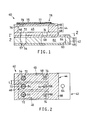
- FIG. 1 schematically showing an inkjet print head 40 as one preferred embodiment of the present invention
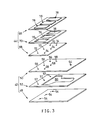
- Fig. 3 which is an exploded perspective view of the print head 40
- an ink nozzle member 42 and an ink pump member 44 are bonded together to form an integral structure of the inkjet print head 40.
- an ink material is supplied to a plurality of ink chambers 46 formed in the ink pump member 44, and is jetted or discharged from a plurality of nozzles 54 formed through the ink nozzle member 42.
- the ink nozzle member 42 consists of a nozzle plate 48 and an orifice plate 50 having a relatively small thickness, and a channel plate 52 interposed between these plates 48, 50.
- the nozzle plate 48 and the orifice plate 50 are integrally bonded to the channel plate 52 by means of an adhesive.
- the nozzle plate 48 has a plurality of nozzles 54 (three in this embodiment) formed therethrough, for permitting jets of fine ink particles, while the orifice plate 50 and the channel plate 52 have respective through-holes 56, 57 formed through the thicknesses thereof. These through-holes 56, 57 are aligned with the respective nozzles 54 as viewed in the direction of the thickness of the plates 48, 50, 52, and have a diameter which is larger by a given value than that of the nozzles 54.
- the orifice plate 50 further has a plurality of orifices 58 (three in this embodiment) formed therethrough, for permitting flow of the ink into to the respective ink chambers 46.
- the channel plate 52 is formed with a window 60 which is closed at its opposite openings by the nozzle plate 48 and orifice plate 50, respectively, whereby an ink supply channel 62 communicating with the orifices 58 is defined by the channel plate 52, the nozzle plate 48 and the orifice plate 50.
- the orifice plate 50 further has a supply port 64 through which the ink is fed from an ink reservoir into the ink supply channel 62.
- each of the orifices 58 is desirably formed in tapered shape such that the diameter of the orifice 58 is reduced in the direction of flow of the ink (i.e., the direction from the ink supply channel 62 toward the ink chambers 46), as shown in Fig. 1 by way of example, so as to function as a check valve for inhibiting the ink from flowing in the reverse direction.
- the ink pump member 44 consists of a closure plate 66 and a connecting plate 68 having a relatively small thickness, and a spacer plate 70 interposed between these plates 66,68. These plates 66,68,70 are superposed on each other and formed integrally into the ink pump member44 in a manneras described later.
- the connecting plate 68 has first communication holes 72 and second communication holes 74 formed therethrough, which are respectively aligned with the through-holes 56 and orifices 58 formed in the orifice plate 50, as viewed in the direction of thickness of the plates 68,50.
- the diameter of the first communication holes 72 is substantially equal to or sl ig htly larger than that of the through-holes 56, while the diameter of the second communication holes 74 is larger by a given value than that of the orifices 58.
- the spacer plate 70 has a plurality of rectangular windows 76 formed therethrough.
- the spacer plate 70 is superposed on the connecting plate 68 such that each of the windows 76 communicates with the corresponding first and second communication holes 72, 74 formed in the connecting plate 68.
- the ink chambers 46 are formed within the ink pump member44, such that the chambers 46 communicate with an exterior space through the first and second communication holes 72, 74.
- the ink pump member 44 is formed as an integrally formed fired ceramic structure. That is, in the process of producing the ink pump member 44, green sheets are initially formed by using a slurry that is prepared from ceramic materials, binders, liquid solvents and others, by means of a generally used device such as a doctor blade device or a reverse roll coater. Then, the green sheets are subjected to suitable processing such as cutting, machining or punching, as needed, so as to form the windows 76 and the first and second communication holes 72, 74. Thus, there are formed precursors for the plates 66, 68, 70. These precursors are then laminated on each other and fired into an integral ceramic body as the ink pump member 44.
- the closure plate 66 preferably has a thickness of 50 ⁇ m or smaller, more preferably, within a range of about 3 to 12wm.
- the connecting plate 68 preferably has a thickness of 10 ⁇ m or larger, more preferably, 50 ⁇ m or larger.
- the spacer plate 70 preferably has a thickness of 50 ⁇ m or larger, more preferably, 100 ⁇ m or larger.
- ink pump member 44 which is formed as an integral fired ceramic structure, does not require any particular adhesive treatment for bonding the plates 66, 68, 70 together. Accordingly, complete and secure sealing can be achieved at the interfaces between the closure plate 66 and spacer plate 70 and between the connecting plate 68 and spacer plate 70.
- the ink pump member 44 can be produced with improved efficiency, due to the presence of the connecting plate 68.
- the laminar structure including the connecting plate 68 exhibits an enhanced rigidity due to the presence of the plate 68, assuring improved handling ease thereof, while reducing the possibility of occurrence of defectives due to handling failure, as compared with when the structure does not include the connecting plate 68.
- the connecting plate 68 makes it possible to handle the laminar structure even in the above-described situation.
- the surface of the ink pump member 44 which is to be bonded to the ink nozzle member42, that is, the outer surface of the connecting plate 68, is made even or smooth.
- the evenness of the relevant surface of the ink pump member44 is suitably controlled so that the surface has the maximum waviness of not larger than 50pm as measured along a reference length of 8mm, by means of a roughness measuring system.
- the maximum waviness of the relevant surface is not larger than 25 ⁇ m, more desirably, not larger than 10 ⁇ m.
- the fired ceramic body which gives the ink pump member44 may be subjected to machining such as lapping or surface grinding.
- piezoelectric/electrostrictive elements 78 which correspond to the respective ink chambers 46 formed in the member 44.
- Each of the piezoelectric/electrostrictive elements 78 has a piezoelectric/electrostrictive unit consisting of a lower electrode 77, a piezoelectric/electrostrictive layer 79, and an upper electrode 75, which are formed in lamination on the closure plate 66, by a suitable film-forming method.
- the piezoelectric/electrostrictive element 78 of the instant embodiment it is particularly preferable to employ a piezoelectric/electrostrictive element as proposed in EP-A-0 526 048 A1.
- the closure plate 66 which serves as a substrate for the piezoelectric/electrostrictive elements 78, is suitably formed by a ceramic substrate made of a material whose major component is zirconia having a crystal phase that is partially or fully stabilized by a suitable compound or compounds.
- the term "partially orfully stabilized zirconia” used herein should be interpreted to mean zirconia whose crystal phase is partially or fully stabilized, so that the crystal phase partially undergoes or does not undergo phase transformations, respectively, upon application of heat, stress or the like thereto.
- the above-indicated compound or compounds for stabilizing the zirconia is selected from the group consisting of: yttrium oxide; cerium oxide; magnesium oxide; and calcium oxide.
- the zirconia is partially or fully stabilized as desired, by addition of at least one of these compounds, that is, a selected one of the above-indicated oxides or a selected combination of two or more of these oxides. It is desirable to stabilize the zirconia by adding 2 to 7 mole % of yttrium oxide, or 6 to 15 mole % of cerium oxide, or 5 to 12 mole % of magnesium oxide or calcium oxide.
- the zirconia has a primary crystal phase which is partially stabilized as a tetragonal phase or a combination of a cubic phase and the tetragonal phase, to provide the ceramic substrate (closure plate 66) having excellent properties.
- the average crystal grain size of the ceramic substrate is preferably controlled to within a range of 0.05wm - 2wm, more preferably, to 1 wm or smaller, so as to ensure the presence of the tetragonal phase and assure a sufficiently large mechanical strength of the ceramic substrate.
- suitable films of the upper and lower electrodes 75, 77 and the piezoelectric/electrostrictive layers 79 are formed on the outer surface of the closure plate 66 by any one of various known methods which include thick-film forming process such as screen printing, spraying, dipping and coating, and thin-film forming process such as ion-beam method, sputtering, vacuum vapor deposition, ion plating, CVD and plating.
- thick-film forming process such as screen printing, spraying, dipping and coating
- thin-film forming process such as ion-beam method, sputtering, vacuum vapor deposition, ion plating, CVD and plating.
- These layers 75, 77, 79 may be formed either before or after firing of the closure plate 66 (the ink pump member 44).
- the electrode films 75, 77 and piezoelectric/electrostrictive layer 79 thus formed on the closure plate 66 may be heat-treated as needed, either in different steps following formation of the respective layers 75, 77, 79, or in one step following formation of all of the layer 75, 77, 79.
- an insulating resin layer between the adjacent piezoelectric/electrostrictive layers 79, 79 may be formed as needed.
- each piezoelectric/ electrostrictive unit may be formed of any electrically conductive material which can withstand a high- temperature oxidizing atmosphere generated upon the heat-treatment or firing as described above.
- the electrode films 75, 77 may be formed of a single metal, an alloy of metals, a mixture of a metal or alloy and an electrically insulating ceramic or glass, or an electrically conductive ceramic.
- the electrode material has as a major component a noble metal having a high melting point, such as platinum, palladium or rhodium, or an alloy such as silver-palladium alloy, silver-platinum alloy or platinum-palladium alloy.
- each piezoelectric/electrostrictive unit may be formed of any piezoelectric or electrostrictive material which produces a relatively large amount of strain or displacement due to the converse or reverse piezoelectric effect or the electrostrictive effect.
- the piezoelectric/electrostrictive material may be either a crystalline material or an amorphous material, and may be a semi-conductor material or a dielectric orferroelectric ceramic material. Further, the piezoelectric/electrostrictive material may either require a treatment for initial polarization or poling, or may not require such a polarization treatment.
- the piezoelectric/electrostrictive material used for the piezoelectric/electrostrictive layer 79 preferably contains as a major component lead zirconate titanate (PZT), lead magnesium niobate (PMN), lead nickel niobate (PNN), lead manganese niobate, lead antimony stannate, lead zinc niobate, lead titanate, or a mixture thereof.
- PZT lead zirconate titanate
- PMN lead magnesium niobate
- PNN lead nickel niobate
- lead manganese niobate lead antimony stannate
- lead zinc niobate lead titanate
- a mixture thereof lead zirconate titanate
- the piezoelectric/electrostrictive material having the above major component may further contain as an additive an oxide or other compound of lanthanum, barium, niobium, zinc, cerium, cadnium, chromium, cobalt, strontium, antimony, iron, yttrium, tantalum, tungsten, nickel, and/or manganese, so as to provide a material containing PLZT, for example.
- an oxide or other compound of lanthanum, barium, niobium, zinc, cerium, cadnium, chromium, cobalt, strontium, antimony, iron, yttrium, tantalum, tungsten, nickel, and/or manganese so as to provide a material containing PLZT, for example.
- the piezoelectric/electrostrictive unit consisting of the electrode films 75, 77 and the piezoelectric/ electrostrictive layer 79 generally has a thickness of not larger than 100 ⁇ m.
- the thickness of each of the electrode films 75, 77 is generally 20pm or smaller, preferably 5 ⁇ m or smaller.
- the thickness of the piezoelectric/electrostrictive layer 79 is preferably 50pm or smaller, more preferably, within a range of 3pm to 40 ⁇ m.
- the substrate of the piezoelectric/ electrostrictive element 78 is constituted by the closure plate 66 formed of a material having partially stabilized zirconia as a major component, the element 78 exhibits sufficiently high degrees of mechanical strength and toughness even though the plate 66 has a relatively small thickness.
- the thus formed piezoelectric/ electrostrictive element 78 can provide a relatively large amount of displacement by application of a relatively low operating voltage, with a relatively large magnitude of force or electric potential generated, and has an improved operating response.
- the film-forming method used for forming the electrode films 75, 77 and the piezoelectric/ electrostrictive layer 79 permits a relatively large number of the piezoelectric/electrostrictive elements 78 to be formed on the closure plate 66 of the ink pump member44. That is, in the film-forming process as described above, the elements 78 can be concurrently and easily formed with a minute spacing left between the adjacent ones, without using an adhesive or the like. Accordingly, a plurality of piezoelectric/electrostrictive elements 78 can be easily formed on appropriation portions of the ink pump member 44 which correspond to the respective ink chambers 46 formed therein.
- the ink pump member 44 After firing the above-described ink pump member 44 on which the piezoelectric/electrostrictive elements 78 are integrally formed, the ink pump member 44 is superposed on the above-described ink nozzle member 42, and these members 42, 44 are bonded together by a suitable adhesive, into an integral structure of the inkjet print head 40, as shown in Fig. 1.
- the ink material which is led through the ink supply channel 62 is supplied to the ink chambers 46 through the respective orifices 58, and is passed through the through-holes 56, 57 and jetted outwards from the nozzles 54, based on the operation of the piezoelectric/electrostrictive elements 78 formed integrally on the ink pump member 44.
- the adhesive used for bonding the ink pump member 44 and ink nozzle member 42 may be selected from various known adhesives containing any one of vinyl, acryl, polyamide, phenol, resorcinol, urea, melamine, polyester, epoxy, furan, polyurethane, silicone, rubber, polyimide and polyolefin, provided the selected adhesive is resistant to the ink material.
- the adhesive is in the form of a highly viscous paste which can be applied by coating using a dispenser, or by screen-printing, or is in the form of a sheet which permits punching thereof. It is more desirable to use a hot-melt type adhesive which requires a relatively short heating time, or an adhesive which is curable at room temperature.
- the adhesive in the form of a highly viscous paste may be obtained by mixing an adhesive material with a filler so as to increase the viscosity of the resulting adhesive.
- an elastic epoxy adhesive or silicone-contained adhesive which can be applied by screen-printing, or sheet-like, hot-melt type adhesive containing polyolefin or polyester, which permits punching thereof. It is also possible to apply various adhesives as indicated above to different portions of the bonding surfaces of the ink pump member 44 and/or the ink nozzle member 42.
- the ink chambers 46 formed in the ink pump member 44 are suitably held in communication with the nozzles 54 and the ink supply channel 62 formed in the ink nozzle member42, with the first and second communication holes 72, 74 being in communication with the through-holes 56 and orifices 58 formed through the orifice plate 50 of the ink nozzle member 42, respectively.
- the seal between the bonding surfaces of the ink pump member 44 and the ink nozzle member 42 needs to be well established only at around the first and second communication holes 72, 74. This leads to a significantly reduced area of bonded portions which must provide a complete seal, permitting the ink flow channel to easily and surely assure excellent fluid-tightness.
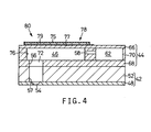
- the diameters of the first and second communication holes 72, 74 are set to be smaller than the width dimension of the ink chamber 46 (the width dimension of the window 76 formed in the spacer plate 70). Therefore, the adjacent ones of the first communication holes 72 and those of the second communication holes 74 are spaced apart from each other by a sufficiently large distance (indicated by "L" in Fig. 2).
- the above arrangement assures a sufficiently large area of bonding between the ink pump member 44 and the ink nozzle member 42, at around the respective first and second communication holes 72, 74. Accordingly, a further improved seal can be obtained at the bonding surfaces of the members 42,44 even if these members 42, 44 are made of different kinds of materials.
- the adhesive overflows into the first and second communication holes 72, 74 to thereby close the openings of these holes 72, 74.
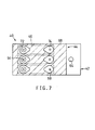
- the diameter of the first and second communication holes 72, 74 be set to be substantially equal to the width dimension of the corresponding ink chamber 46, so as to avoid the closure of the openings of the holes 72, 74. It is also desirable to form one or both of the first and second communication holes 72 in teardrop shape as shown in Fig. 7, or elliptic shape.
- the ink jet print head 40 can easily and stably assure sufficient sealing or fluid-tightness of the ink flow channel through which the ink flows, without suffering from the overflow of the adhesive into the ink chambers 46, and otherwise possible gaps formed between the bonding surfaces.
- the ink jet print head 40 exhibits significantly improved ink-jetting characteristics.
- the piezoelectric/electrostrictive elements 78 each of which is adapted to deform a portion of the closure member 66 which defines the corresponding ink chamber 46 to thereby change the internal pressure of the ink chamber 46. Therefore, the piezoelectric/electrostrictive elements 78 can be easily formed on the portions of the closure member 66 which correspond to the respective ink chambers 46, with high production efficiency, assuring excellent ink-jetting characteristics of the print head with high stability.
- the ink supply channel 62 through which the ink is fed into the ink chambers 46 is formed within the ink nozzle member42 in the illustrated embodiment
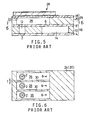
- the inksupplychannel62 may be formed within the ink pump member 44, as shown in Fig. 4 by way of example.
- the same numerals as used in Fig. 1 showing the first embodiment are used for identifying structurally or functionally corresponding elements, so as to facilitate understanding of the embodiment of Fig. 4.
- the structure and material of the ink nozzle member42 are by no means limited to those of the illustrated embodiment. For instance, it is possible to form the whole or a part of the ink nozzle member 42 as an integral body, by injection molding using a synthetic resin material or the like, or any other molding technique.
- the position and number of the nozzles 54 and orifices 58 formed in the ink nozzle member 42, and the position and number of the ink chambers 46 formed in the ink pump member 44 are never limited to those of the illustrated embodiment, but may be suitably selected.
- the principle of the present invention is applicable to inkjet print heads of on-demand type or continuous jet type, and to these types of ink jet print heads having various structures.
Applications Claiming Priority (4)
| Application Number | Priority Date | Filing Date | Title |
|---|---|---|---|
| JP16020492 | 1992-05-27 | ||
| JP160204/92 | 1992-05-27 | ||
| JP08799693A JP3144948B2 (ja) | 1992-05-27 | 1993-03-22 | インクジェットプリントヘッド |
| JP87996/93 | 1993-03-22 |
Publications (3)
| Publication Number | Publication Date |
|---|---|
| EP0572231A2 true EP0572231A2 (de) | 1993-12-01 |
| EP0572231A3 EP0572231A3 (de) | 1994-04-06 |
| EP0572231B1 EP0572231B1 (de) | 1996-10-09 |
Family
ID=26429215
Family Applications (1)
| Application Number | Title | Priority Date | Filing Date |
|---|---|---|---|
| EP93304070A Expired - Lifetime EP0572231B1 (de) | 1992-05-27 | 1993-05-26 | Tintenstrahldruckkopf |
Country Status (6)
| Country | Link |
|---|---|
| US (1) | US5933170A (de) |
| EP (1) | EP0572231B1 (de) |
| JP (1) | JP3144948B2 (de) |
| DE (1) | DE69305232T2 (de) |
| HK (1) | HK24297A (de) |
| SG (1) | SG48850A1 (de) |
Cited By (18)
| Publication number | Priority date | Publication date | Assignee | Title |
|---|---|---|---|---|
| EP0659562A2 (de) * | 1993-12-24 | 1995-06-28 | Seiko Epson Corporation | Lamellenartig aufgebauter Tintenstrahlaufzeichnungskopf |
| EP0661156A2 (de) * | 1993-12-28 | 1995-07-05 | Seiko Epson Corporation | Tintenstrahlaufzeichnungskopf |
| EP0732208A1 (de) * | 1995-03-06 | 1996-09-18 | Ngk Insulators, Ltd. | Tintendruckkopf mit keramischer Tintenpumpe und damit verbundenem metallischen Düsenkörper |
| EP0744388A1 (de) * | 1995-05-26 | 1996-11-27 | Ngk Insulators, Ltd. | Verfahren zur Herstellung eines keramischen Körpers mit kleinen durchgehenden Löchern |
| EP0695638A3 (de) * | 1994-08-04 | 1997-02-12 | Seiko Epson Corp | Tintenstrahlaufzeichnungskopf |
| EP0785071A1 (de) * | 1995-07-24 | 1997-07-23 | Seiko Epson Corporation | Chip des piezoelektrischen/elektrostriktiven types |
| EP0799699A2 (de) * | 1996-04-04 | 1997-10-08 | Seiko Epson Corporation | Laminierter Tintenstrahlaufzeichnungskopf |
| EP0829355A1 (de) * | 1996-03-28 | 1998-03-18 | Sony Corporation | Drucker |
| EP0830945A1 (de) * | 1996-04-04 | 1998-03-25 | Sony Corporation | Druckvorrichtung und verfahren zur herstellung |
| US5764258A (en) * | 1994-08-20 | 1998-06-09 | Eastman Kodak Company | Print head with integrated pump |
| EP0987111A2 (de) * | 1995-11-10 | 2000-03-22 | Seiko Epson Corporation | Antreibseinheit |
| US6270203B1 (en) * | 1992-08-26 | 2001-08-07 | Seiko Epson Corporation | Multilayer ink jet recording head having a pressure generating unit and a flow path unit |
| EP1209467A2 (de) * | 2000-11-22 | 2002-05-29 | Xerox Corporation | Vorrichtungen zum Ausstossen einer biologischen Flüssigkeit |
| US6485275B1 (en) | 1998-07-02 | 2002-11-26 | Ngk Insulators, Ltd. | Device for discharging raw material-fuel |
| US6533197B1 (en) | 1998-07-03 | 2003-03-18 | Ngk Insulators, Ltd. | Device for discharging raw material-fuel |
| US6601949B1 (en) | 1992-08-26 | 2003-08-05 | Seiko Epson Corporation | Actuator unit for ink jet recording head |
| WO2004085064A2 (en) * | 2002-10-15 | 2004-10-07 | Wisconsin Alumni Research Foundation | Methods and apparata for precisely dispensing microvolumes of fluids |
| EP2957607A1 (de) * | 2014-06-17 | 2015-12-23 | Konica Minolta, Inc. | Bilderzeugungsverfahren |
Families Citing this family (69)
| Publication number | Priority date | Publication date | Assignee | Title |
|---|---|---|---|---|
| US6004644A (en) * | 1994-07-26 | 1999-12-21 | Ngk Insulators, Ltd. | Zirconia diaphragm structure and piezoelectric/electrostrictive film element having the zirconia diaphragm structure |
| JP3196811B2 (ja) * | 1994-10-17 | 2001-08-06 | セイコーエプソン株式会社 | 積層型インクジェット式記録ヘッド、及びその製造方法 |
| JP3890634B2 (ja) * | 1995-09-19 | 2007-03-07 | セイコーエプソン株式会社 | 圧電体薄膜素子及びインクジェット式記録ヘッド |
| US6217158B1 (en) | 1996-04-11 | 2001-04-17 | Seiko Epson Corporation | Layered type ink jet recording head with improved piezoelectric actuator unit |
| JP3386108B2 (ja) * | 1997-01-24 | 2003-03-17 | セイコーエプソン株式会社 | インクジェット式記録ヘッド |
| JP3414227B2 (ja) * | 1997-01-24 | 2003-06-09 | セイコーエプソン株式会社 | インクジェット式記録ヘッド |
| US6494566B1 (en) | 1997-01-31 | 2002-12-17 | Kyocera Corporation | Head member having ultrafine grooves and a method of manufacture thereof |
| US7320457B2 (en) * | 1997-02-07 | 2008-01-22 | Sri International | Electroactive polymer devices for controlling fluid flow |
| US6891317B2 (en) * | 2001-05-22 | 2005-05-10 | Sri International | Rolled electroactive polymers |
| US6628040B2 (en) * | 2000-02-23 | 2003-09-30 | Sri International | Electroactive polymer thermal electric generators |
| EP0928688A4 (de) | 1997-07-03 | 2000-10-18 | Matsushita Electric Ind Co Ltd | Tintenstrahlaufzeichnungskopf und verfahren zur herstellung |
| JP3236536B2 (ja) * | 1997-07-18 | 2001-12-10 | 日本碍子株式会社 | セラミック基体及びこれを用いたセンサ素子 |
| JP3727781B2 (ja) | 1998-07-03 | 2005-12-14 | 日本碍子株式会社 | 原料・燃料用吐出装置 |
| JP3241334B2 (ja) * | 1998-11-16 | 2001-12-25 | 松下電器産業株式会社 | インクジェットヘッド及びその製造方法 |
| JP2001018395A (ja) * | 1999-07-02 | 2001-01-23 | Canon Inc | 液体吐出ヘッドおよびその製造方法 |
| US7537197B2 (en) * | 1999-07-20 | 2009-05-26 | Sri International | Electroactive polymer devices for controlling fluid flow |
| JP3700049B2 (ja) | 1999-09-28 | 2005-09-28 | 日本碍子株式会社 | 液滴吐出装置 |
| US6755511B1 (en) * | 1999-10-05 | 2004-06-29 | Spectra, Inc. | Piezoelectric ink jet module with seal |
| US6726312B1 (en) | 1999-10-12 | 2004-04-27 | Kabushiki Kaisha Giken | Ink jet head for use in a printer |
| JP2001186881A (ja) | 1999-10-22 | 2001-07-10 | Ngk Insulators Ltd | Dnaチップの製造方法 |
| JP2001186880A (ja) | 1999-10-22 | 2001-07-10 | Ngk Insulators Ltd | Dnaチップの製造方法 |
| ATE340027T1 (de) | 1999-10-22 | 2006-10-15 | Ngk Insulators Ltd | Flüssigkeitsspender zur herstellung von dna- mikroarrays |
| US6656432B1 (en) | 1999-10-22 | 2003-12-02 | Ngk Insulators, Ltd. | Micropipette and dividedly injectable apparatus |
| ATE358277T1 (de) | 1999-10-22 | 2007-04-15 | Ngk Insulators Ltd | Dna-chip und verfahren zur herstellung desselben |
| JP3492570B2 (ja) * | 1999-10-22 | 2004-02-03 | 日本碍子株式会社 | マイクロピペット及び分注装置 |
| JP3389987B2 (ja) * | 1999-11-11 | 2003-03-24 | セイコーエプソン株式会社 | インクジェット式記録ヘッド及びその製造方法 |
| US6362558B1 (en) | 1999-12-24 | 2002-03-26 | Kansai Research Institute | Piezoelectric element, process for producing the same and ink jet recording head |
| US6676250B1 (en) | 2000-06-30 | 2004-01-13 | Silverbrook Research Pty Ltd | Ink supply assembly for a print engine |
| US6740530B1 (en) | 2000-11-22 | 2004-05-25 | Xerox Corporation | Testing method and configurations for multi-ejector system |
| US6861034B1 (en) | 2000-11-22 | 2005-03-01 | Xerox Corporation | Priming mechanisms for drop ejection devices |
| US20020085067A1 (en) * | 2000-12-29 | 2002-07-04 | Robert Palifka | Ink jet printing module |
| US7407746B2 (en) | 2001-02-08 | 2008-08-05 | Ngk Insulators, Ltd. | Biochip and method for producing the same |
| DE60223667T2 (de) | 2001-05-01 | 2009-01-02 | Ngk Insulators, Ltd., Nagoya | Verfahren zur herstellung eines biochips |
| US7233097B2 (en) * | 2001-05-22 | 2007-06-19 | Sri International | Rolled electroactive polymers |
| JP3689030B2 (ja) * | 2001-09-05 | 2005-08-31 | 日本碍子株式会社 | 複合ノズル、液滴吐出装置、およびこれらの製造方法 |
| US20030116641A1 (en) * | 2001-10-02 | 2003-06-26 | Ngk Insulators, Ltd. | Liquid injection apparatus |
| EP1300585A3 (de) | 2001-10-02 | 2003-06-18 | Ngk Insulators, Ltd. | Einspritzvorrichtung für Flüssigkeit |
| JP2003214302A (ja) | 2001-11-16 | 2003-07-30 | Ngk Insulators Ltd | 液体燃料噴射装置 |
| TW537498U (en) * | 2002-02-08 | 2003-06-11 | Ritdisplay Corp | Package structure of organic light emitting diode panel |
| JP4221184B2 (ja) * | 2002-02-19 | 2009-02-12 | 日本碍子株式会社 | マイクロ化学チップ |
| JP3957528B2 (ja) * | 2002-03-05 | 2007-08-15 | 日本碍子株式会社 | 圧電/電歪膜型素子 |
| DK1481467T3 (da) * | 2002-03-05 | 2010-10-11 | Stanford Res Inst Int | Elektroaktive polymerapparater til styring af en fluidumstrøm |
| JP2005522162A (ja) * | 2002-03-18 | 2005-07-21 | エスアールアイ インターナショナル | 流体を移動させる電気活性ポリマーデバイス |
| CN101054020B (zh) * | 2002-04-09 | 2010-09-29 | 精工爱普生株式会社 | 液体喷头 |
| KR100421026B1 (ko) * | 2002-04-29 | 2004-03-04 | 삼성전자주식회사 | 잉크젯 프린트헤드 제조방법 |
| US6796637B2 (en) * | 2002-05-28 | 2004-09-28 | Ngk Insulators, Ltd. | Piezoelectric/electrostrictive film type actuator and method for manufacturing the same |
| US7086154B2 (en) * | 2002-06-26 | 2006-08-08 | Brother Kogyo Kabushiki Kaisha | Process of manufacturing nozzle plate for ink-jet print head |
| US7052117B2 (en) | 2002-07-03 | 2006-05-30 | Dimatix, Inc. | Printhead having a thin pre-fired piezoelectric layer |
| JP4095005B2 (ja) * | 2003-09-16 | 2008-06-04 | 日本碍子株式会社 | Dnaチップの製造方法 |
| US8491076B2 (en) | 2004-03-15 | 2013-07-23 | Fujifilm Dimatix, Inc. | Fluid droplet ejection devices and methods |
| US7281778B2 (en) | 2004-03-15 | 2007-10-16 | Fujifilm Dimatix, Inc. | High frequency droplet ejection device and method |
| WO2006074016A2 (en) | 2004-12-30 | 2006-07-13 | Fujifilm Dimatix, Inc. | Ink jet printing |
| JP4529739B2 (ja) * | 2005-03-09 | 2010-08-25 | 富士フイルム株式会社 | 液体吐出ヘッド、画像形成装置及び液体吐出ヘッドの製造方法 |
| KR100727937B1 (ko) * | 2005-06-01 | 2007-06-13 | 삼성전자주식회사 | 잉크 카트리지의 어레이 헤드 본딩 방법 |
| US7988247B2 (en) | 2007-01-11 | 2011-08-02 | Fujifilm Dimatix, Inc. | Ejection of drops having variable drop size from an ink jet printer |
| EP2174360A4 (de) | 2007-06-29 | 2013-12-11 | Artificial Muscle Inc | Wandler mit elektroaktivem polymer für anwendungen der sensorischen rückmeldung |
| EP2239793A1 (de) | 2009-04-11 | 2010-10-13 | Bayer MaterialScience AG | Elektrisch schaltbarer Polymerfilmaufbau und dessen Verwendung |
| JP2012020422A (ja) * | 2010-07-12 | 2012-02-02 | Seiko Epson Corp | 液体噴射ヘッド、液体噴射ヘッドユニット及び液体噴射装置 |
| KR20140008416A (ko) | 2011-03-01 | 2014-01-21 | 바이엘 인텔렉쳐 프로퍼티 게엠베하 | 변형가능한 중합체 장치 및 필름을 제조하기 위한 자동화 제조 방법 |
| US9195058B2 (en) | 2011-03-22 | 2015-11-24 | Parker-Hannifin Corporation | Electroactive polymer actuator lenticular system |
| WO2013142552A1 (en) | 2012-03-21 | 2013-09-26 | Bayer Materialscience Ag | Roll-to-roll manufacturing processes for producing self-healing electroactive polymer devices |
| WO2013192143A1 (en) | 2012-06-18 | 2013-12-27 | Bayer Intellectual Property Gmbh | Stretch frame for stretching process |
| US9590193B2 (en) | 2012-10-24 | 2017-03-07 | Parker-Hannifin Corporation | Polymer diode |
| JP2014193550A (ja) * | 2013-03-28 | 2014-10-09 | Seiko Epson Corp | 液体噴射ヘッドおよび液体噴射装置 |
| JP2014193583A (ja) | 2013-03-29 | 2014-10-09 | Seiko Epson Corp | 液体吐出ヘッド、液体吐出装置、及び液体吐出ヘッドの製造方法 |
| JP2014198398A (ja) * | 2013-03-29 | 2014-10-23 | セイコーエプソン株式会社 | 流路ユニット、液体吐出ヘッド、液体吐出装置、流路ユニットの製造方法 |
| JP2018103376A (ja) * | 2016-12-22 | 2018-07-05 | セイコーエプソン株式会社 | 液体噴射ヘッド、及び、液体噴射装置 |
| US11912041B2 (en) | 2021-12-17 | 2024-02-27 | Ricoh Company, Ltd. | Printhead with internal pump at fluid manifold |
| WO2023157127A1 (ja) * | 2022-02-16 | 2023-08-24 | コニカミノルタ株式会社 | インクジェットヘッド及びインクジェット記録装置 |
Citations (4)
| Publication number | Priority date | Publication date | Assignee | Title |
|---|---|---|---|---|
| GB2182611A (en) * | 1985-11-06 | 1987-05-20 | Pitney Bowes Inc | Impulse ink jet print head and methods of making the same |
| US4695854A (en) * | 1986-07-30 | 1987-09-22 | Pitney Bowes Inc. | External manifold for ink jet array |
| US4937597A (en) * | 1988-02-16 | 1990-06-26 | Fuji Electric Co., Ltd. | Ink jet printing head |
| EP0443628A2 (de) * | 1990-02-23 | 1991-08-28 | Seiko Epson Corporation | Auf Abruf arbeitender Tintenstrahldruckknopf |
Family Cites Families (16)
| Publication number | Priority date | Publication date | Assignee | Title |
|---|---|---|---|---|
| US3946398A (en) * | 1970-06-29 | 1976-03-23 | Silonics, Inc. | Method and apparatus for recording with writing fluids and drop projection means therefor |
| SE349676B (de) * | 1971-01-11 | 1972-10-02 | N Stemme | |
| JPS58116163A (ja) * | 1981-12-29 | 1983-07-11 | Canon Inc | 液体噴射ヘツド |
| JPS60232967A (ja) * | 1984-05-04 | 1985-11-19 | Nec Corp | インクジエツトヘツド |
| US4766671A (en) * | 1985-10-29 | 1988-08-30 | Nec Corporation | Method of manufacturing ceramic electronic device |
| JPS62101455A (ja) * | 1985-10-29 | 1987-05-11 | Nec Corp | インクジエツトヘツドとその製造方法 |
| JPS62213399A (ja) * | 1986-03-12 | 1987-09-19 | Omron Tateisi Electronics Co | 圧電磁器 |
| DE3628346A1 (de) * | 1986-08-21 | 1988-02-25 | Siemens Ag | Tintendruckkopf in dickschichttechnik |
| JPS63149159A (ja) * | 1986-12-12 | 1988-06-21 | Fuji Electric Co Ltd | インクジエツト記録ヘツド |
| WO1989007752A1 (en) * | 1988-02-22 | 1989-08-24 | Spectra, Inc. | Pressure chamber for ink jet systems |
| JP2842448B2 (ja) * | 1989-07-11 | 1999-01-06 | 日本碍子株式会社 | 圧電/電歪膜型アクチュエータ |
| US5087930A (en) * | 1989-11-01 | 1992-02-11 | Tektronix, Inc. | Drop-on-demand ink jet print head |
| JPH07108102B2 (ja) * | 1990-05-01 | 1995-11-15 | 日本碍子株式会社 | 圧電/電歪膜型アクチュエータの製造方法 |
| DE69129159T2 (de) * | 1990-11-09 | 1998-07-16 | Citizen Watch Co Ltd | Tintenstrahlkopf |
| JP3144949B2 (ja) * | 1992-05-27 | 2001-03-12 | 日本碍子株式会社 | 圧電/電歪アクチュエータ |
| JP3106026B2 (ja) * | 1993-02-23 | 2000-11-06 | 日本碍子株式会社 | 圧電/電歪アクチュエータ |
-
1993
- 1993-03-22 JP JP08799693A patent/JP3144948B2/ja not_active Expired - Lifetime
- 1993-05-26 SG SG1996003036A patent/SG48850A1/en unknown
- 1993-05-26 EP EP93304070A patent/EP0572231B1/de not_active Expired - Lifetime
- 1993-05-26 DE DE69305232T patent/DE69305232T2/de not_active Expired - Lifetime
-
1997
- 1997-01-02 US US08/735,445 patent/US5933170A/en not_active Expired - Lifetime
- 1997-02-27 HK HK24297A patent/HK24297A/xx not_active IP Right Cessation
Patent Citations (4)
| Publication number | Priority date | Publication date | Assignee | Title |
|---|---|---|---|---|
| GB2182611A (en) * | 1985-11-06 | 1987-05-20 | Pitney Bowes Inc | Impulse ink jet print head and methods of making the same |
| US4695854A (en) * | 1986-07-30 | 1987-09-22 | Pitney Bowes Inc. | External manifold for ink jet array |
| US4937597A (en) * | 1988-02-16 | 1990-06-26 | Fuji Electric Co., Ltd. | Ink jet printing head |
| EP0443628A2 (de) * | 1990-02-23 | 1991-08-28 | Seiko Epson Corporation | Auf Abruf arbeitender Tintenstrahldruckknopf |
Cited By (48)
| Publication number | Priority date | Publication date | Assignee | Title |
|---|---|---|---|---|
| US6290340B1 (en) | 1992-05-19 | 2001-09-18 | Seiko Epson Corporation | Multi-layer ink jet print head and manufacturing method therefor |
| US6929354B2 (en) | 1992-08-26 | 2005-08-16 | Seiko Epson Corp | Multi-layer ink jet recording head and manufacturing method therefor |
| US6270203B1 (en) * | 1992-08-26 | 2001-08-07 | Seiko Epson Corporation | Multilayer ink jet recording head having a pressure generating unit and a flow path unit |
| US6601949B1 (en) | 1992-08-26 | 2003-08-05 | Seiko Epson Corporation | Actuator unit for ink jet recording head |
| EP0659562A2 (de) * | 1993-12-24 | 1995-06-28 | Seiko Epson Corporation | Lamellenartig aufgebauter Tintenstrahlaufzeichnungskopf |
| EP1170127A2 (de) * | 1993-12-24 | 2002-01-09 | Seiko Epson Corporation | Tintenstrahlaufzeichnungskopf |
| EP1170127A3 (de) * | 1993-12-24 | 2002-05-08 | Seiko Epson Corporation | Tintenstrahlaufzeichnungskopf |
| EP0659562A3 (de) * | 1993-12-24 | 1996-02-07 | Seiko Epson Corp | Lamellenartig aufgebauter Tintenstrahlaufzeichnungskopf. |
| US6502929B1 (en) | 1993-12-24 | 2003-01-07 | Seiko Epson Corporation | Laminated ink jet recording head having a plurality of actuator units |
| US6893117B2 (en) | 1993-12-24 | 2005-05-17 | Seiko Epson Corporation | Laminated ink jet recording head |
| US6902262B2 (en) | 1993-12-24 | 2005-06-07 | Seiko Epson Corporation | Laminated ink jet recording head |
| US5880756A (en) * | 1993-12-28 | 1999-03-09 | Seiko Epson Corporation | Ink jet recording head |
| US6206501B1 (en) | 1993-12-28 | 2001-03-27 | Seiko Epson Corporation | Ink jet recording head |
| EP0812692A3 (de) * | 1993-12-28 | 1998-01-07 | Seiko Epson Corporation | Tintenstrahlaufzeichnungskopf |
| EP0812692A2 (de) * | 1993-12-28 | 1997-12-17 | Seiko Epson Corporation | Tintenstrahlaufzeichnungskopf |
| EP0661156A2 (de) * | 1993-12-28 | 1995-07-05 | Seiko Epson Corporation | Tintenstrahlaufzeichnungskopf |
| EP0661156A3 (de) * | 1993-12-28 | 1996-05-15 | Seiko Epson Corp | Tintenstrahlaufzeichnungskopf. |
| US5748214A (en) * | 1994-08-04 | 1998-05-05 | Seiko Epson Corporation | Ink jet recording head |
| EP0695638A3 (de) * | 1994-08-04 | 1997-02-12 | Seiko Epson Corp | Tintenstrahlaufzeichnungskopf |
| US5764258A (en) * | 1994-08-20 | 1998-06-09 | Eastman Kodak Company | Print head with integrated pump |
| EP0732208A1 (de) * | 1995-03-06 | 1996-09-18 | Ngk Insulators, Ltd. | Tintendruckkopf mit keramischer Tintenpumpe und damit verbundenem metallischen Düsenkörper |
| CN1090565C (zh) * | 1995-03-06 | 2002-09-11 | 日本碍子株式会社 | 带有陶瓷墨泵部件以及金属喷嘴部件的喷墨打印头 |
| US5728244A (en) * | 1995-05-26 | 1998-03-17 | Ngk Insulators, Ltd. | Process for production of ceramic member having fine throughholes |
| EP0744388A1 (de) * | 1995-05-26 | 1996-11-27 | Ngk Insulators, Ltd. | Verfahren zur Herstellung eines keramischen Körpers mit kleinen durchgehenden Löchern |
| EP0785071A1 (de) * | 1995-07-24 | 1997-07-23 | Seiko Epson Corporation | Chip des piezoelektrischen/elektrostriktiven types |
| EP0785071A4 (de) * | 1995-07-24 | 1997-10-08 | Seiko Epson Corp | Chip des piezoelektrischen/elektrostriktiven types |
| US6440174B1 (en) | 1995-07-24 | 2002-08-27 | Seiko Epson Corporation | Piezo-electric/electrostrictive film type chip |
| EP0987111A3 (de) * | 1995-11-10 | 2000-04-12 | Seiko Epson Corporation | Antriebseinheit |
| EP0987111A2 (de) * | 1995-11-10 | 2000-03-22 | Seiko Epson Corporation | Antreibseinheit |
| US6176571B1 (en) | 1996-03-28 | 2001-01-23 | Sony Corporation | Printer |
| EP0829355A4 (de) * | 1996-03-28 | 1998-12-09 | Sony Corp | Drucker |
| EP0829355A1 (de) * | 1996-03-28 | 1998-03-18 | Sony Corporation | Drucker |
| EP1010532A2 (de) * | 1996-04-04 | 2000-06-21 | Sony Corporation | Drucker und Verfahren zu seiner Herstellung |
| EP0830945A4 (de) * | 1996-04-04 | 1998-12-09 | Sony Corp | Druckvorrichtung und verfahren zur herstellung |
| US6109737A (en) * | 1996-04-04 | 2000-08-29 | Sony Corporation | Printer device and the manufacturing method |
| EP1010532A3 (de) * | 1996-04-04 | 2000-07-05 | Sony Corporation | Drucker und Verfahren zu seiner Herstellung |
| EP0799699A2 (de) * | 1996-04-04 | 1997-10-08 | Seiko Epson Corporation | Laminierter Tintenstrahlaufzeichnungskopf |
| US6024436A (en) * | 1996-04-04 | 2000-02-15 | Seiko Epson Corporation | Laminated ink jet recording head |
| EP0830945A1 (de) * | 1996-04-04 | 1998-03-25 | Sony Corporation | Druckvorrichtung und verfahren zur herstellung |
| EP0799699A3 (de) * | 1996-04-04 | 1998-12-23 | Seiko Epson Corporation | Laminierter Tintenstrahlaufzeichnungskopf |
| US6485275B1 (en) | 1998-07-02 | 2002-11-26 | Ngk Insulators, Ltd. | Device for discharging raw material-fuel |
| US6533197B1 (en) | 1998-07-03 | 2003-03-18 | Ngk Insulators, Ltd. | Device for discharging raw material-fuel |
| EP1209467A3 (de) * | 2000-11-22 | 2004-01-14 | Xerox Corporation | Vorrichtungen zum Ausstossen einer biologischen Flüssigkeit |
| EP1209467A2 (de) * | 2000-11-22 | 2002-05-29 | Xerox Corporation | Vorrichtungen zum Ausstossen einer biologischen Flüssigkeit |
| WO2004085064A2 (en) * | 2002-10-15 | 2004-10-07 | Wisconsin Alumni Research Foundation | Methods and apparata for precisely dispensing microvolumes of fluids |
| WO2004085064A3 (en) * | 2002-10-15 | 2004-12-16 | Wisconsin Alumni Res Found | Methods and apparata for precisely dispensing microvolumes of fluids |
| US7467751B2 (en) | 2002-10-15 | 2008-12-23 | Wisconsin Alumni Research Foundation | Methods and apparata for precisely dispensing microvolumes of fluids |
| EP2957607A1 (de) * | 2014-06-17 | 2015-12-23 | Konica Minolta, Inc. | Bilderzeugungsverfahren |
Also Published As
| Publication number | Publication date |
|---|---|
| EP0572231A3 (de) | 1994-04-06 |
| EP0572231B1 (de) | 1996-10-09 |
| DE69305232D1 (de) | 1996-11-14 |
| SG48850A1 (en) | 1998-05-18 |
| US5933170A (en) | 1999-08-03 |
| DE69305232T2 (de) | 1997-03-20 |
| JP3144948B2 (ja) | 2001-03-12 |
| JPH0640030A (ja) | 1994-02-15 |
| HK24297A (en) | 1997-02-27 |
Similar Documents
| Publication | Publication Date | Title |
|---|---|---|
| EP0572231B1 (de) | Tintenstrahldruckkopf | |
| US5475279A (en) | Piezoelectric/electrostrictive actuator having integral ceramic base member and film-type piezoelectric/electrostrictive element (S) | |
| US6290340B1 (en) | Multi-layer ink jet print head and manufacturing method therefor | |
| EP0587346B1 (de) | Farbstrahldruckkopf mit Bestandteilen mit verschiedenen Wärme-Ausdehnungskoeffizienten | |
| EP0600743B1 (de) | Antriebselement mit keramischem Substrat und Tintenstrahldruckkopf mit Benützung derselben | |
| JP3106026B2 (ja) | 圧電/電歪アクチュエータ | |
| EP0666605B1 (de) | Piezoelektrischer und/oder elektrostriktiver Antrieb | |
| US5831651A (en) | Ink jet print head having ceramic ink pump member whose thin orifice plate is reinforced by thick reinforcing plate, and metallic nozzle member bonded to the orifice or reinforcing plate | |
| JP2014014967A (ja) | 液滴吐出ヘッド、インクカートリッジ及び画像形成装置 | |
| CN101638004B (zh) | 液体喷射头和液体喷射装置及压电元件 | |
| US6997547B2 (en) | Piezoelectric element, piezoelectric actuator and liquid jetting head incorporating the same | |
| US7591544B2 (en) | Liquid ejecting head, method of producing the same, and liquid ejecting apparatus | |
| JPH06312505A (ja) | 積層型圧電変位素子及びそれを用いたインクジェット記録ヘッド | |
| US20020196314A1 (en) | Piezoelectric transducer | |
| JP3363881B2 (ja) | インクジェットプリントヘッド | |
| JP2001047623A (ja) | インクジェットプリンターヘッド | |
| US6440174B1 (en) | Piezo-electric/electrostrictive film type chip | |
| JP2001179975A (ja) | 圧電/電歪アクチュエータ | |
| JP3106030B2 (ja) | 圧電/電歪アクチュエータ | |
| JP2002086726A (ja) | 静電気式機械作動流体マイクロメタリング装置 |
Legal Events
| Date | Code | Title | Description |
|---|---|---|---|
| PUAI | Public reference made under article 153(3) epc to a published international application that has entered the european phase |
Free format text: ORIGINAL CODE: 0009012 |
|
| 17P | Request for examination filed |
Effective date: 19930615 |
|
| AK | Designated contracting states |
Kind code of ref document: A2 Designated state(s): DE FR GB IT |
|
| PUAL | Search report despatched |
Free format text: ORIGINAL CODE: 0009013 |
|
| AK | Designated contracting states |
Kind code of ref document: A3 Designated state(s): DE FR GB IT |
|
| RAP1 | Party data changed (applicant data changed or rights of an application transferred) |
Owner name: SEIKO EPSON CORPORATION Owner name: NGK INSULATORS, LTD. |
|
| 17Q | First examination report despatched |
Effective date: 19950814 |
|
| GRAH | Despatch of communication of intention to grant a patent |
Free format text: ORIGINAL CODE: EPIDOS IGRA |
|
| GRAH | Despatch of communication of intention to grant a patent |
Free format text: ORIGINAL CODE: EPIDOS IGRA |
|
| GRAA | (expected) grant |
Free format text: ORIGINAL CODE: 0009210 |
|
| AK | Designated contracting states |
Kind code of ref document: B1 Designated state(s): DE FR GB IT |
|
| REF | Corresponds to: |
Ref document number: 69305232 Country of ref document: DE Date of ref document: 19961114 |
|
| ET | Fr: translation filed | ||
| ITF | It: translation for a ep patent filed |
Owner name: MODIANO & ASSOCIATI S.R.L. |
|
| PLBE | No opposition filed within time limit |
Free format text: ORIGINAL CODE: 0009261 |
|
| STAA | Information on the status of an ep patent application or granted ep patent |
Free format text: STATUS: NO OPPOSITION FILED WITHIN TIME LIMIT |
|
| 26N | No opposition filed | ||
| RIN2 | Information on inventor provided after grant (corrected) |
Free format text: TAKEUCHI, YUKIHISA * MASUMORI, HIDEO * TAKAHASHI, NOBUO * SONEHARA, HIDEAKI * KITAHARA, KOHEI |
|
| REG | Reference to a national code |
Ref country code: FR Ref legal event code: RN |
|
| REG | Reference to a national code |
Ref country code: GB Ref legal event code: IF02 |
|
| PGFP | Annual fee paid to national office [announced via postgrant information from national office to epo] |
Ref country code: DE Payment date: 20120531 Year of fee payment: 20 |
|
| PGFP | Annual fee paid to national office [announced via postgrant information from national office to epo] |
Ref country code: FR Payment date: 20120510 Year of fee payment: 20 Ref country code: GB Payment date: 20120426 Year of fee payment: 20 |
|
| PGFP | Annual fee paid to national office [announced via postgrant information from national office to epo] |
Ref country code: IT Payment date: 20120521 Year of fee payment: 20 |
|
| REG | Reference to a national code |
Ref country code: DE Ref legal event code: R071 Ref document number: 69305232 Country of ref document: DE |
|
| REG | Reference to a national code |
Ref country code: DE Ref legal event code: R071 Ref document number: 69305232 Country of ref document: DE |
|
| REG | Reference to a national code |
Ref country code: GB Ref legal event code: PE20 Expiry date: 20130525 |
|
| PG25 | Lapsed in a contracting state [announced via postgrant information from national office to epo] |
Ref country code: DE Free format text: LAPSE BECAUSE OF EXPIRATION OF PROTECTION Effective date: 20130528 Ref country code: GB Free format text: LAPSE BECAUSE OF EXPIRATION OF PROTECTION Effective date: 20130525 |