EP0516185A2 - Integrierte Halbleiterschaltungen Vorrichtung von Scheibengrösse - Google Patents
Integrierte Halbleiterschaltungen Vorrichtung von Scheibengrösse Download PDFInfo
- Publication number
- EP0516185A2 EP0516185A2 EP19920112517 EP92112517A EP0516185A2 EP 0516185 A2 EP0516185 A2 EP 0516185A2 EP 19920112517 EP19920112517 EP 19920112517 EP 92112517 A EP92112517 A EP 92112517A EP 0516185 A2 EP0516185 A2 EP 0516185A2
- Authority
- EP
- European Patent Office
- Prior art keywords
- semiconductor
- pillar
- substrate
- memory
- wafer
- Prior art date
- Legal status (The legal status is an assumption and is not a legal conclusion. Google has not performed a legal analysis and makes no representation as to the accuracy of the status listed.)
- Granted
Links
Images


Classifications
-
- H—ELECTRICITY
- H10—SEMICONDUCTOR DEVICES; ELECTRIC SOLID-STATE DEVICES NOT OTHERWISE PROVIDED FOR
- H10W—GENERIC PACKAGES, INTERCONNECTIONS, CONNECTORS OR OTHER CONSTRUCTIONAL DETAILS OF DEVICES COVERED BY CLASS H10
- H10W70/00—Package substrates; Interposers; Redistribution layers [RDL]
- H10W70/60—Insulating or insulated package substrates; Interposers; Redistribution layers
- H10W70/611—Insulating or insulated package substrates; Interposers; Redistribution layers for connecting multiple chips together
-
- H—ELECTRICITY
- H10—SEMICONDUCTOR DEVICES; ELECTRIC SOLID-STATE DEVICES NOT OTHERWISE PROVIDED FOR
- H10W—GENERIC PACKAGES, INTERCONNECTIONS, CONNECTORS OR OTHER CONSTRUCTIONAL DETAILS OF DEVICES COVERED BY CLASS H10
- H10W70/00—Package substrates; Interposers; Redistribution layers [RDL]
- H10W70/60—Insulating or insulated package substrates; Interposers; Redistribution layers
- H10W70/67—Insulating or insulated package substrates; Interposers; Redistribution layers characterised by their insulating layers or insulating parts
- H10W70/69—Insulating materials thereof
- H10W70/698—Semiconductor materials that are electrically insulating, e.g. undoped silicon
-
- H—ELECTRICITY
- H10—SEMICONDUCTOR DEVICES; ELECTRIC SOLID-STATE DEVICES NOT OTHERWISE PROVIDED FOR
- H10W—GENERIC PACKAGES, INTERCONNECTIONS, CONNECTORS OR OTHER CONSTRUCTIONAL DETAILS OF DEVICES COVERED BY CLASS H10
- H10W78/00—Detachable holders for supporting packaged chips in operation
-
- H—ELECTRICITY
- H10—SEMICONDUCTOR DEVICES; ELECTRIC SOLID-STATE DEVICES NOT OTHERWISE PROVIDED FOR
- H10W—GENERIC PACKAGES, INTERCONNECTIONS, CONNECTORS OR OTHER CONSTRUCTIONAL DETAILS OF DEVICES COVERED BY CLASS H10
- H10W90/00—Package configurations
-
- H—ELECTRICITY
- H10—SEMICONDUCTOR DEVICES; ELECTRIC SOLID-STATE DEVICES NOT OTHERWISE PROVIDED FOR
- H10W—GENERIC PACKAGES, INTERCONNECTIONS, CONNECTORS OR OTHER CONSTRUCTIONAL DETAILS OF DEVICES COVERED BY CLASS H10
- H10W90/00—Package configurations
- H10W90/401—Package configurations characterised by multiple insulating or insulated package substrates, interposers or RDLs
-
- H—ELECTRICITY
- H10—SEMICONDUCTOR DEVICES; ELECTRIC SOLID-STATE DEVICES NOT OTHERWISE PROVIDED FOR
- H10W—GENERIC PACKAGES, INTERCONNECTIONS, CONNECTORS OR OTHER CONSTRUCTIONAL DETAILS OF DEVICES COVERED BY CLASS H10
- H10W72/00—Interconnections or connectors in packages
- H10W72/20—Bump connectors, e.g. solder bumps or copper pillars; Dummy bumps; Thermal bumps
- H10W72/29—Bond pads specially adapted therefor
-
- H—ELECTRICITY
- H10—SEMICONDUCTOR DEVICES; ELECTRIC SOLID-STATE DEVICES NOT OTHERWISE PROVIDED FOR
- H10W—GENERIC PACKAGES, INTERCONNECTIONS, CONNECTORS OR OTHER CONSTRUCTIONAL DETAILS OF DEVICES COVERED BY CLASS H10
- H10W72/00—Interconnections or connectors in packages
- H10W72/50—Bond wires
- H10W72/531—Shapes of wire connectors
- H10W72/536—Shapes of wire connectors the connected ends being ball-shaped
-
- H—ELECTRICITY
- H10—SEMICONDUCTOR DEVICES; ELECTRIC SOLID-STATE DEVICES NOT OTHERWISE PROVIDED FOR
- H10W—GENERIC PACKAGES, INTERCONNECTIONS, CONNECTORS OR OTHER CONSTRUCTIONAL DETAILS OF DEVICES COVERED BY CLASS H10
- H10W72/00—Interconnections or connectors in packages
- H10W72/50—Bond wires
- H10W72/541—Dispositions of bond wires
- H10W72/5434—Dispositions of bond wires the connected ends being on auxiliary connecting means on bond pads, e.g. on other bond wires
-
- H—ELECTRICITY
- H10—SEMICONDUCTOR DEVICES; ELECTRIC SOLID-STATE DEVICES NOT OTHERWISE PROVIDED FOR
- H10W—GENERIC PACKAGES, INTERCONNECTIONS, CONNECTORS OR OTHER CONSTRUCTIONAL DETAILS OF DEVICES COVERED BY CLASS H10
- H10W72/00—Interconnections or connectors in packages
- H10W72/50—Bond wires
- H10W72/551—Materials of bond wires
- H10W72/552—Materials of bond wires comprising metals or metalloids, e.g. silver
- H10W72/5522—Materials of bond wires comprising metals or metalloids, e.g. silver comprising gold [Au]
-
- H—ELECTRICITY
- H10—SEMICONDUCTOR DEVICES; ELECTRIC SOLID-STATE DEVICES NOT OTHERWISE PROVIDED FOR
- H10W—GENERIC PACKAGES, INTERCONNECTIONS, CONNECTORS OR OTHER CONSTRUCTIONAL DETAILS OF DEVICES COVERED BY CLASS H10
- H10W72/00—Interconnections or connectors in packages
- H10W72/50—Bond wires
- H10W72/551—Materials of bond wires
- H10W72/552—Materials of bond wires comprising metals or metalloids, e.g. silver
- H10W72/5524—Materials of bond wires comprising metals or metalloids, e.g. silver comprising aluminium [Al]
-
- H—ELECTRICITY
- H10—SEMICONDUCTOR DEVICES; ELECTRIC SOLID-STATE DEVICES NOT OTHERWISE PROVIDED FOR
- H10W—GENERIC PACKAGES, INTERCONNECTIONS, CONNECTORS OR OTHER CONSTRUCTIONAL DETAILS OF DEVICES COVERED BY CLASS H10
- H10W72/00—Interconnections or connectors in packages
- H10W72/50—Bond wires
- H10W72/59—Bond pads specially adapted therefor
-
- H—ELECTRICITY
- H10—SEMICONDUCTOR DEVICES; ELECTRIC SOLID-STATE DEVICES NOT OTHERWISE PROVIDED FOR
- H10W—GENERIC PACKAGES, INTERCONNECTIONS, CONNECTORS OR OTHER CONSTRUCTIONAL DETAILS OF DEVICES COVERED BY CLASS H10
- H10W72/00—Interconnections or connectors in packages
- H10W72/851—Dispositions of multiple connectors or interconnections
- H10W72/874—On different surfaces
- H10W72/884—Die-attach connectors and bond wires
-
- H—ELECTRICITY
- H10—SEMICONDUCTOR DEVICES; ELECTRIC SOLID-STATE DEVICES NOT OTHERWISE PROVIDED FOR
- H10W—GENERIC PACKAGES, INTERCONNECTIONS, CONNECTORS OR OTHER CONSTRUCTIONAL DETAILS OF DEVICES COVERED BY CLASS H10
- H10W72/00—Interconnections or connectors in packages
- H10W72/90—Bond pads, in general
- H10W72/951—Materials of bond pads
-
- H—ELECTRICITY
- H10—SEMICONDUCTOR DEVICES; ELECTRIC SOLID-STATE DEVICES NOT OTHERWISE PROVIDED FOR
- H10W—GENERIC PACKAGES, INTERCONNECTIONS, CONNECTORS OR OTHER CONSTRUCTIONAL DETAILS OF DEVICES COVERED BY CLASS H10
- H10W90/00—Package configurations
- H10W90/701—Package configurations characterised by the relative positions of pads or connectors relative to package parts
- H10W90/721—Package configurations characterised by the relative positions of pads or connectors relative to package parts of bump connectors
- H10W90/724—Package configurations characterised by the relative positions of pads or connectors relative to package parts of bump connectors between a chip and a stacked insulating package substrate, interposer or RDL
-
- H—ELECTRICITY
- H10—SEMICONDUCTOR DEVICES; ELECTRIC SOLID-STATE DEVICES NOT OTHERWISE PROVIDED FOR
- H10W—GENERIC PACKAGES, INTERCONNECTIONS, CONNECTORS OR OTHER CONSTRUCTIONAL DETAILS OF DEVICES COVERED BY CLASS H10
- H10W90/00—Package configurations
- H10W90/701—Package configurations characterised by the relative positions of pads or connectors relative to package parts
- H10W90/731—Package configurations characterised by the relative positions of pads or connectors relative to package parts of die-attach connectors
- H10W90/734—Package configurations characterised by the relative positions of pads or connectors relative to package parts of die-attach connectors between a chip and a stacked insulating package substrate, interposer or RDL
Definitions
- the present invention relates to the packaging of semiconductor integrated circuits, and more particularly to a packaging technique for semiconductor integrated circuits formed on a large-sized semiconductor substrate such as a semiconductor wafer.
- semiconductor integrated circuits are constructed on respective parts of a substate, i.e. a semiconductor wafer chip the wafer then being subdivided by dicing it into a plurality of parts each corresponding to one or more integrated circuits.
- a semiconductor wafer chip the wafer then being subdivided by dicing it into a plurality of parts each corresponding to one or more integrated circuits.
- Recently constructions have been investigated in which the semiconductor wafer is not subdivided, but a plurality of integrated circuits are fabricated on the whole of the semiconductor wafer so as to construct a large-sized semiconductor integrated circuit.
- Such a semiconductor manufacturing technique is described in e.g. Japanese patent KOKAI (Disclosure) 61-290739, in which one large-sized semiconductor integrated circuit is constructed on the entire semiconductor wafer.
- the present invention proposes a packaging device which engages such wafer(s) and thereby holds them in place.
- the device can then hold the wafers in a spaced-apart relationship.
- a semiconductor memory device fabricated by a wager sized very LSI has been proposed from, for instance Japanese patent KOKAI (Disclosure) application No. 59-201441.
- the cutting of the defective chips and removal of these defective chips are performed by such a way that fuses, or power source lines are cut out by irradiating focused ion beams, or laser light rays, and only those chips without defects are connected by the final wiring.
- fuses, or power source lines are cut out by irradiating focused ion beams, or laser light rays, and only those chips without defects are connected by the final wiring.
- a large number of manufacturing stages and thus, a large number of masks are required. As a result, the throughput is not improved and the cost is high.
- one or more redundant blocks for removing the defects is built in the memory system body within the wafer so that to increase the redundancy, the total area which the entire system body occupies must be reduced. If a faulty block is to be discovered by means of probing, the lower throughput must be accepted. In some cases, such a probing check may cause another defect.
- the present invention seeks to provide a wafer-sized semiconductor integrated circuit device which permits a more satisfactory defect relieving method.
- a semiconductor integrated circuit device has a plurality of circuit blocks having specific circuit functions, whereby the block addresses are allocated so as to designate the respective circuit blocks.
- a wafer-scale semiconductor integrated circuit device comprising a plurality of circuit blocks each having a specific circuit function, whereby a block address for designating the respective circuit blocks is allocated.
- a plurality of semiconductor memory circuits may be provided, including a decoder circuit as the circuit block and a memory array selected by the decoder circuit.
- a control circuit may then be allocated to the respective semiconductor memory circuits, which performs a selection operation based on the block address.
- the selection operation in the semiconductor memory circuit is prohibited by the block address due to existence of a defect.
- the wafer-scale integrated circuit device may be constructed of a plurality of memory mats, a memory array section of the semiconductor memory circuit being subdivided. Then, a preliminary memory circuit having a decoder circuit corresponding to the memory mat is arranged around a peripheral section of a wafer, and when a defect is present, the selection of the preliminary memory circuit is performed, and the selection of the semiconductor circuit is prohibited.
- control circuit functions to output externally the block address of the semiconductor substrate containing the defect.
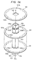
- an integrated circuit region 101A on which various integrated circuits have been constructed is present on a surface of a large-sized semiconductor substrate 101 made of a semiconductor wafer.
- a rectangular opening 102 which has been formed by, for instance, etching treatment, is formed.
- the semiconductor substrate 101 is supported by an upper supporting member 105A and a lower supporting member 105B made of, e.g., an epoxy resin in such a manner that, a rectangular pillar 102 made of, for instance, an alminium alloy or a plastic resin is pierced through the opening 102, and the substrate is sandwiched by both the upper and lower supporting members 105A and 105B formed on the four sides of the pillar 103.
- the central portion of this pillar 103 is made empty.
- a size of the opening 102 of the substrate 101 is defined under the condition that the pillar 103 can be substantially penetrated through the opening 102 while both the upper and lower supporting members 105A and 105B are bent toward the pillar side.
- the pillar 103 is made of a metal such as aluminium, the surface of the metal pillar is covered with a resin so as to electrically insulate the wiring leads.
- a plurality of connector pins 104 are formed on the bottom of the pillar 103 so as to package the pillar 103 which mounts a plurality of semiconductor substrates 101, on a packaging substrate (not shown).
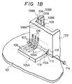
- Both the upper and lower supporting members 105A and 105B have such a shape that, as illustrated in Figs. 1B and 1C, each edge thereof located at the pillar 103 is engaged with a supporting projection 103A which projects from the pillar 103.
- a hole 119 for penetrating a supporting shaft 114 therethrough is formed on the upper supporting member 105A, lower supporting member 105B, and supporting projection 103A, respectively. That is to say, both the upper and lower supporting members 105A and 105B are mounted on the supporting projection 103A in such a manner that they can be rotated with respect to the supporting axis 114 as its rotating center.
- a twist coil spring 112 is arranged on both sides of the upper and lower supporting members 105A and 105B, one end 112A of the twist coil spring 112 is fixed to either the upper supporting member 105A or lower supporting member 105B, and the supporting shaft 114 is penetrated through a central hole 113 thereof. It is seen that only twist coil spring 112 of one edge of the respective upper and lower supporting members 105A and 105B in Figs. 1B and 1C. As a result, the semiconductor substrate 101 is supported by the upper and lower supporting members 105A and 105B by means of the elasticity of the above-described twist coil spring 112.
- a plurality of fixing electrodes are fixed on the upper surface of the upper supporting member 105A, which are made of aluminium on which, for instance, copper or silver is plated.
- a plurality of brush electrodes having elasticity are provided on the side of the pillar 103 corresponding to the fixing electrodes 106, and one end of the respective brush electrodes is resiliently in contact with the surface of the corresponding fixing electrodes 106.
- the end portion of the respective brush electrodes 107 which is resiliently in contact with the respective fixing electrodes, is slidable on the corresponding fixing electrode 106 while the upper supporting members 105A is rotated.
- Another electrode 110 made of, for example, cupper is provided on an inner surface of the pillar 103, in relation to the above-described brush electrode 107, and is connected to the brush electrode 107 by a lead 109 made of, for instance, aluminium on which silver is plated. Between this lead 109 and the pillar 103, an epoxy resin is provided for electrical insulation.
- the insulated cable 108 is attached to the pillar 103 by adhesive agent so that these insulated cables are employed to connect between the respective semiconductor substrates 101 provided on the pillar 103 and also the semiconductor substrate 101 and the connector pin 104 shown in Fig. 1A.
- a spring electrode 115 having elasticity is provided on the upper surface corresponding to the respective fixing electrodes 106 of the upper supporting member 105A.
- a pin 116 made of, for example, silver-plated aluminium is mechanically and electrically connected between the spring electrode and the fixing electrode 106.
- the respective spring electrodes 115 are resiliently in contact with an electrode 120 made of, for example, an aluminium film which is provided on the surface of the semiconductor substrate 101.
- a spring electrode 115 is provided on the lower supporting member 105B in order that it is used as a supporting member for sandwiching the semiconductor substrate 101. That is to say, the semiconductor substrate 101 is supported in such a manner that a plurality of spring electrodes 115 respectively provided on the upper and lower supporting members 105A and 105B sandwich this substrate 101.
- the upper and lower supporting members 105A and 105B are bent toward the pillar by the manual operation.
- a rubber 117 made of, for instance, a sillicone rubber for preventing the horizontal vibrations is employed between the upper supporting member 105A of the pillar 103 and the lower supporting member 105B.
- the pillar 103 may be shaped as a cylinder according to the invention. In this case, it is apparent that the shape of the opening 102 formed on the semiconductor substrate 101 may be circle.
- both rear surfaces of two sheets of the semiconductor substrates 101, on which no integrated circuit 101A is arranged, are connected to each other by the adhesive agent, and thus the connected semiconductor substrates are sandwiched by these upper and lower supporting members 105A and 105B.
- an interval between the upper and lower supporting members 105A and 105B is wider than that of a single semiconductor substrate 105.
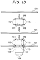
- the packaging device according to the invention may be constructed as a packaging device as shown in Fig. 1D.
- the semiconductor substrate 101 has no opening 102 as illustrated in Figs. 1A to 1C.
- the shape of the pillar 103 is formed as a rectanglar pillar or a cylindircal pillar, the upper and lower edges of which are flat surfaces. That is to say, an interior of the pillar 103 is formed as a cavity, and both the upper and lower ends thereof are made closed.
- the adhesive agent 118 is coated on both the upper and lower ends thereof are made closed.
- the adhesive agent 118 is coated on both the upper and lower ends which are in turn attached to the central portion of the semiconductor substrate 101. No integrated circuit is constructed on the portion to which the pillar 103 of the semiconductor substrate 101 is attached.
- Connecting electrodes (not shown) are employed on both surfaces of the semiconductor substrate 101, corresponding to the electrode 115 mounted on the pillar 103. Electrical connection is made between the electrodes formed on both surfaces of the semiconductor substrate 101 via the connecting hole which penetrates through the semiconductor substrate 101.
- the pillar 103 and semiconductor substrate 101 are alternately stacked from the bottom.
- the packaging device for packaging the large-sized semiconductor substrate in a stable condition can be realized.
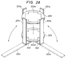
- reference numeral 203 denotes a semiconductor wafer made of a monocrystal silicon and reference numeral 203A indicates an integrated circuit region for constructing various integrated circuits.
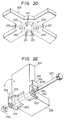
- a packaging device of a semiconductor integrated circuit according to the second embodiment includes pillars 201a, 201b, 201c and 201d standing at a peripheral portion of an integrated wafer 203, and a pillar connecting substrate 202 which is connected to the lower end portions of these pillars 201a to 201d so as to stably stand these pillars.
- the pillar 201 and pillar connecting substrate 202 are made of a resin such as an epoxy resin, or aluminium.
- the semiconductor wafer 203 is sandwiched by semiconductor substrate supporting members 205 and 210 which are provided on the pillar 201.
- the pillars for instance, 201b and 201c are arranged to be bent, or brought down as shown in Fig. 2E.
- the remaining pillars 201a and 201d are fixed on the pillar connecting substrate 202.
- only the pillar 201a, three pillars 201a to 201c, or all of the pillars 201a to 201d may be bent or brought down.
- the pillars 201 other than the bendable pillars 201 are fixed on the pillar connecting substrate 202.
- the semiconductor wafer 203 is supported by the upper semiconductor substrate supporting member 205 and the lower semiconductor substrate supporting member 206 mounted on the pillar 201 in the fixed condition.
- the upper semiconductor substrate supporting member 210 is made of, for instance, a resin such as an epoxy resin, or alminium, and is integrally formed with, for example, the pillar 201.
- the lower semiconductor substrate supporting member 210 is mounted on a supporting section 201A projecting from the pillar 201 in such a manner that it is rotatable around the supporting shaft 212.
- the lower semiconductor substrate supporting member 210 is made of, for instance, a resin such as a glass epoxy resin, or aluminium.
- a plurality of hair-pin-shaped spring electrodes 206 are provided on the lower surface of the upper semiconductor substrate supporting member 205 so as to be resiliently connected to the electrode 204 of the semiconductor wafer 203.
- the spring electrode 206 is connected via an embeded wiring lead 207 which penetrates through the upper semiconductor substrate supporting member 205, and the upper wiring lead 208 of the upper surface of the upper semiconductor substrate supporting member 205, to a terminal electrode 214 provided on the outer wall of the pillar 201.
- the wiring lead 208 penetrates through a through hole formed on the pillar 201.
- the hair-pin-shaped pressure spring 211 is provided on the upper surface of the lower semiconductor substrate supporting member 210, i.e., the plane opposite to the semiconductor wafer 203.
- a handle 213 is mounted on the lower surface of the lower semiconductor substrate supporting member 210 so as to open a space defined between the upper and lower semiconductor substrate supporting members 205 and 210 when mounting the semiconductor wafer 203.
- the above-described upper semiconductor substrate supporting member 205, lower semiconductor substrate supporting member 210, and coil spring 209 are mounted on the corresponding pillars 201a, 201b, 201c and 201d, so that the semiconductor wafer 203 can be sandwiched at four positions under the stable condition.
- the above-described spring electrode 206, wiring leads 207 and 208, coil spring 209 and pressure spring 211 are mounted on the respective upper and lower substrate supporting members 205 and 210 which are mounted on the corresponding four pillars 201. With respect to the spring electrode 206, the electrode 204 is arranged to the semiconductor wafer 203.
- a core 215A of a cable 215 which is insulating-covered with vinyle chloride is connected by solder.
- This insulating cable 215 connects the respective semiconductor wafers 203, and the semiconductor wafers 203 packaged on the packaging substrate and also the wiring lines on the packaging substrate.
- a sandwiching member of the semiconductor wafer 203 is provided in such a manner that the semiconductor wafer supporting, or sandwiching member 205 is ⁇ -shaped, and both the spring electrode 206 and pressure spring 211 are fixed on the side surface of the inside thereof.
- the pillar 201 defines a cavity 218 of a cylindrical form at the portion corresponding to the semiconductor substrate supporting member 205 in order to fit with the semiconductor substrate supporting member 205.
- the semiconductor substrate supporting member 205 fitted within this cavity 218 is positioned to be depressed by the coil spring 219.
- a terminal electrode 217 is provided on the upper surface of the semiconductor substrate supporting member 205, to which the core 215A of the cable 215 is connected.
- the cable 215 extends over the plane opposite to the semiconductor wafer 203, i.e., the outer wall of the pillar 201. This cable 215 is connected via a through hole formed on the pillar 201 adjacent to the semiconductor substrate supporting member 215 to the terminal electrode 216. To achieve the better connection between the spring electrode 206 and the electrode 204 and also firmly sandwich the semiconductor wafer 203, an interval between the spring electrode 206 and pressure spring 211 by which the semiconductor wafer 203 is not yet mounted, is narrower than the thickness of the semiconductor wafer 203.
- FIG. 2E One example of the connection between the lower end portion of the pillar 201 and the pillar connecting substrate 202 is shown in Fig. 2E.
- the connecting portion of the pillar connecting substrate 202 is engaged with the lower portion of the pillar 201, and rotatably connected in such a manner that a mounting bolt 227 is inserted into the corresponding bolt hole 230 formed on these portions.
- the bolt 227 is so arranged that it is not dropped from the corresponding bolt hole 230 by mounting a nut 228 on the screw section 227.
- a twist coil spring 222 is positioned on both sides of the pillar and the bolt 227 is penetrated through the respective center holes 226.
- this twist coil spring 222 is mounted in the spring mounting hole 223 of the pillar connecting substrate 202, whereas the other end thereof is mounted in the spring mounting hole 225 formed on the projection 224 of the pillar 201.
- the pillar 201 can be stood up at a right angle by this twist coil spring 222, and also the bent pillar 201 can be recovered by means of the twist coil spring 222.
- both the pillar 201 and pillar connecting substrate 202 may be constructed as shown in Fig. 2F.
- pillar 201b among four pillars 201 is so arranged to be bent.
- a hinge is mounted between the bent pillar 201b and the pillar connecting substrate 202 at these connecting sections 202A in such a manner that it is mounted between the outer wall of the pillar 201 and the edge portion of the pillar connecting substrate 202. Since the hinge is mounted to the outer wall of the pillar 201b, the pillar is not bent inside, but allowable to be bent outside.
- a lid 229 is employed to cover it.
- the semiconductor substrate supporting members 205 shown in Fig. 2B or 2C and 210 are provided with the pillar 201 illustrated in Fig. 2F.
- Both the rear surfaces of the semiconductor wafer 203, for instance, are attached to each other, and the resultant semiconductor wafers 203 may be supported by either the semiconductor substrate supporting members 205 and 210 (see Fig. 2B), or 205 (Fig. 2C).
- the interval between the semiconductor supporting members 205, 210, and 205, into which the semiconductor wafer 203 can be inserted is made wider than that of the single semiconductor wafer 203.
- the semiconductor wafer 203 is not limited to the above-mentioned wafer, but may be such a semiconductor substrate that, for example, the peripherals of the semiconductor wafer 203 are cut off to form a rectangle-shaped semiconductor wafer.
- the layout for arranging the respective pillars 201, and the size and shape of the pillar connecting substrate 202 may be modified, depending upon the size and shape of the employed semiconductor substrate.
- the packaging device is constructed of a plurality of pillars standing around the peripherals of the semiconductor wafer, the semiconductor substrate supporting members and pillar connecting members and pillar connecting substrate mounted thereto, the semiconductor wafer can be supported thereon without any twist and vibration phenomenon. As a consequence, a large-sized semiconductor integrated circuit constructed of a semiconductor wafer can be packaged under the stable condition.
- the semiconductor device according to the third embodiment is so arranged in that a plurality of semiconductor chips "Chip” made of a single crystal silicon are mounted on a mounting substrate 301 made of a single-crystal semiconductor wafer. Between the respective semiconductor chips "Chip”, there are provided a wiring region 303 consisting of a wiring line 304x made of an aluminium film as a first layer for connecting the semiconductor chips "Chip”, and also a wiring line 304y made of an aluminium film as a second layer. These first and second layers 304x and 304y extend in the wiring region 303.
- the wiring line 304x of the first layer extend over an insulating film 308 of a silicon oxide film which is formed on the mounting substrate 301 by, for instance, the CVD method.
- An insulating film 309 made of a silicon oxide film by, for instance, the CVD method is employed to inslate between the wiring line 304x and the wiring line 304y of the second layer.
- a final protection film 310 made of a silicon oxide film which is processed by, for example, the CVD methods covers the wiring line 304y.
- the connection between the wiring line 304x and wiring line 304y is accomplished by a connecting hole which is formed by removing the insulating film 309.
- a plurality of bonding pads which are constructed by stacking the aluminium film 302x of the first layer and the aluminium film 302y of the second layer.
- the aluminium film 302x is overlaid on the insulating film 308, whereas another aluminium film 302y is connected to the aluminium wiring line 302x via a connecting hole 311 which is formed by removing the insulating film 309.
- Either the above-described wiring line 304x or 304y is connected to the bonding pads 302.
- this wiring line 304x is integrally formed with the aluminium film 302x which constitutes the lower portion of the bonding pad 302.
- this wiring line 304y is integrally formed with the aluminium film 302y which constitutes the upper portion of the bonding pad 302.
- the final protection film 310 has been removed when overlaying the bonding pad 302, and then becomes an opening 312.
- a plurality of bonding pads 305 formed by stacking the aluminium layer 305x of the first layer and the aluminium layer 305y of the second layer.
- the aluminium film 305x is located over the insulating film 308.
- the aluminium film 305y is connected via the connecting hole 311 to another aluminium film 305x.
- the bonding pad 305 is exposed from the opening 312.
- Either wiring line 304x or wiring line 304y is connected to the bonding pad 305.
- the aluminium film 305 constituting the lower portion of this bonding pad 305 is integrally formed with the wiring line 304x.
- the aluminium layer 305y constituting the upper portion of this bonding pad 305 is integrally formed with the wiring line 304y.
- no element such as MISFET, bipolar transistor, resistor element, capacitive element and so on is constructed.
- resistor element or capactive element may be formed on the portion other than the region on which the semiconductor chips "Chip" are mounted in the surface portion of the mounting substrate 301.
- the semiconductor chips "Chip” are attached on the final protection film 310 by means of an adhesive agent 313 such as a sillicone rubber. Stress applied to the semiconductor chips “Chip” can be reduced by introducing the sillicone rubber into the adhesive agent.
- a plurality of bonding pads 307 are arranged around the peripheral of the semiconductor chips “Chip”. This bonding pad 307 is so constructed by stacking up, for instance, the aluminium film of the first layer and the aluminium film of the second layer. It should be noted that a large quantity of MISFET, bipolar transistor, resistor element and capacitive element are provided on the surface of the semiconductor chips "Chip".
- a field insulating film made of a silicon oxide film is formed by way of, for instance, thermal oxidation.
- wiring lines made of a poly-crystal silicon film formed by the CVD method (treatment), or an aluminium film formed by the sputtering treatment are extended.
- An insulating film made of a silicon oxide film formed by, for example, the CVD treatment is employed to made an electrical insulation between the upper wiring line and the lower wiring line.
- an insulating film of a first layer which is made of a silicon oxide film formed by, for instance, the CVD method, and covers, for example the MISFET's gate electrode.
- the upper portions of the semiconductor chips "ChiP" are covered with a final protection film 314 which is formed by stacking a silicon oxide film, and a coating glass (SOG) film by way of the CVD method, or a silicon nitride film by way of the sputtering treatment.
- This final protection film 314 has been selectively removed on the bonding pad 307 so that it becomes an opening 315.
- a bonding wire is connected, which is made of an aluminium wire on which, for instance, a gold wire and a silver wire have been plated.
- the connection between the bonding wire 306 and the bonding pad 307, and also the bonding wire 306 and the bonding pad 305, is performed by means of, for instance, the ultrasonic bonding, thermal contacting and so on.
- This bonding wire 316 is connected to a lead 320 made of a 42 alloy, as illustrated in Fig. 3D.
- Fig. 3D there is shown a sectional view of the mounting substrate 301, the package substrate 318A for sealing the semiconductor chips "Chip” and the package cap 318B.
- the packaging substrate 318A is made of, for instance, ceramics, and alumina etc.
- the package cap 318B is made of, for example, ceramics.
- the mounting substrate 301 is attached to the packaging cap 318A by means of the adhesive agent 317 made of, for instance, a sillicone rubber. By employing the sillicone rubber into the adhesive agent 317, stress applied to the mounting substrate 301 made of a single crystal silicon can be reduced.
- the packaging substrate 318A is attached to the package cap 318B by means of a sealing agent 319 made of, for instance, glass. A gap between the packaging substrate 318A and the packaging cap 318B formed by a lead 320 is sealed by the sealing agent 319.
- the adhersive connection between the semiconductor chips “Chip” and the mounting substrate 301 may be accomplished in such a manner that the insulating films 308 and 309 underneath the semiconductor chips “Chip”, and the final protection film 310 are selectively removed to expose the surface of the mounting substrate 301, and these semiconductor chips “ChiP" are connected to the exposed region by means of the adhesive agent 313.
- the adhesive connection between the semiconductor chips "ChiP" and the mounting substrate 301 may be accomplished by employing, for example, an Au paste.
- the electrical connection between the semiconductor chips "Chip” and the mounting substrate 301 is performed by employing the bonding pad 307, bonding wire 306 and bonding pad 305, the reliability on the electrical connection between the semiconductor chips "Chip” and the mounting substrate 301 can be improved due to the fact that the rigid connection between these parts is established.
- the heat produced in the semiconductor chips "Chip” can be radiated via the mounting substrate 301 to the packaging substrate 318A,and furthermore to the atmosphere. This implies that the higher heat radiation effect can be realized because the semiconductor chips "Chip” are not separated from the mounting substrate 301. This effect can be specifically improved in such a semiconductor device where a plurality of semiconductor chips "Chip” are sealed within the same package (318A, 318B).
- the mounting substrate 301 is made of the same material, i.e., single crystal silicon as that of the semiconductor chips "Chip", a difference in the thermal expansion between these elements can be reduced to zero.
- the mounting substrate 301 is used as the semiconductor wafer, no the stress concentration onto the mounting substrate 301 is introduced so that no damage is made in the mounting substrate 301, which can improve the reliability.
- the mounting substrate 301 is not made from the semiconductor wafer, but may be formed as a rectangular mounting substrate 301, the peripheral portions of which are cut off.
- the semiconductor integrated circuit device may be built within an IC card.
- the size of the mounting substrate 301 is made small enough to store the mounting substrate 301 within the IC card, so that a plurality of semiconductor chips "Chip" are mounted thereon.
- the bonding wire 306, and the bonding pads 307 and 305 are employed to connect between this semiconductor chip "Chip” and the mounting substrate 301.
- the semiconductor integrated circuit device is not sealed in the package substrates 318A and 318B, but stored in the IC card.
- the bonding wire is employed to connect between the semiconductor chip and the mounting substrate, the reliability on the electrical connection between the semiconductor chip and the mounting substrate can be improved.
- the heat generated in the semiconductor chip can be radiated via the mounting substrate to the package, and in turn in the atmosphere. In other words, the radiation effect can be improved.
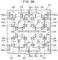
- FIG. 4A there is shown a block diagram of a fourth embodiment in which the present invention is applied to a wafer-scale semiconductor memory device.
- Each of the circuit blocks shown in Fig. 4A is formed based upon the known manufacturing technique for a semiconductor integrated circuit.
- Each of the circuit blocks shown in Fig. 4A is drawn, taking account of the practical geometric circuit arrangement on a wafer-scale WSI (wafer-scale semiconductor integrated circuit device).
- the memory blocks MO to M29 are not specifically limited, but are constructed of memory arrays constituting dynamic type RAM's, and also decoder circuits for performing their selecting operation. That is to say, as shown in Fig 4B, the memory block Mi is, briefly speaking, constructed of a memory array, a column decoder CDCR for selecting its data line (bit line, or digit line), and a row decoder RDCR for selecting its word line. As represented by a dotted line in Fig. 4A, the memory array is subdivided into two memory mats, in principle. A sense amplifier SA is arranged on each center portion of the respective memory mats.
- a switch circuit may be employed for selectively connecting this sense amplifier to either memory mat (not shown in detail).
- a column switch circuit may be provided in parallel to this sense amplifier.
- the above-described memory block Mi includes various circuits (not shown in detail). These arrangements of the memory array and the address selecting circuit may be constructed of the circuit equivalent to the known dynamic type RAM. In the preferred embodiment, the memory array is also subdivided vertically to obtain two divided portions as illustrated in Fig. 4, for the sake of convenience.
- the above-described memory blocks M0 to M29 require a relatively large rectangular area to be occupied. Accordingly, an empty space is produced around the peripheral portion of a substantially circular wafer WSI.
- the above-described preliminary memory circuit RM is so designed as to occupy a relative smaller area where there are a memory array section corresponding to the memory mats subdivided from one memory block, and a decoder circuit thereof.
- a large quantity of the above-described preliminary memory circuits RM are formed at the peripheral portion of the wafer on which the memory block Mi required to have the relatively large occupied area can be formed.
- Such a circuit arrangement can prevent the practical memory capacity from being reduced when adding the redundant circuit. In other words, while adding the redundant functions, the memory system owning the larger memory capacity can be obtained.
- a control circuit CONT may be arranged at a position corresponding to an orientation flat section of the wafer WSI.
- This control circuit CONT performs the selection operation of the above-described memory block Mi by receiving address signals BA and MA and a control signal TC supplied from the external source.
- an electrode to be connected to the above external terminal is provided on the above-described orientation flat section. This electrode is utilized for the probing when the memory system constituted by the above-described memory block circuit RM and also control circuit CONT formed on the wafer WSI is accomplished.
- the address signal BA among the above-described address signals corresponds to a block address signal for designating one memory blocks M0 to M29.
- the address signal MA corresponds to an address signal commonly supplied to the above-described respective memory blocks M0 to M29. Therefore, the control circuit CONT includes a decoder circuit for producing a selection signal for one memory block, while receiving the above-described block address signal BA. Between the above-described control circuit CONT and the respective memory blocks M0 to M29, there are arranged an address supply line for supplying the above-described common address signal MA, a signal line for supplying and receiving a read/write signal between the respective memory blocks M0 to M29, a timing signal for controlling various operations, and a selecting signal line formed by decoding the above-described block address signal BA. Due to complex circuitry, such signal lines are omitted in the figures.
- an address supply line for supplying an address signal with respect to the above-described preliminary memory circuit RM, a signal line for receiving/supplying a read/write signal between the respective preliminary memory circuits RM, and a signal line for the same timing signal and selection signal as in the above case,
- the preliminary memory circuit RM has only 1/4 memory capacity, as compared with the memory capacity of one ememory block Mi, the addredd setting operation and also the allocation of the selecting signal line can be performed by a program.
- the address signal except for the respective most significant bits of the row/column with respect to the above-described memory block Mi, is supplied to the respective decoder circuits.
- the selection signal line for the respective preliminary memory circuits RM is provided in one-to-one correspondence with the control circuit CONT. This selecting signal line is designated by combining the block address signal designated under control of the control circuit CONT with the remaining higher 2-bit address signal. As a consequence, one preliminary memory circuit RM is allocated to the address block and the higher 2-bit memory address by the address designation at the control circuit CONT.
- control circuit CONT performs the memory access with respect to the respective memory blocks M0 to M29 and owns such a function that while judging whether or not the defect is present, it sends out externally a failed address signal NA(block address) corresponding to the failed memory block.
- the operation per se of the above-described memory system is similar to that of the conventional board-arranged memory device wherein the memory block is constructed of one semiconductor integrated circuit device, and the wafer WSI is substituted by a printed substrate.
- the block addresses are allocated to the respective memory blocks.
- the memory block Mi essentially containing such a defect can be separated by invalidate the corresponding selection signal.
- the power supply line should be separated by projecting the laser ray, as similarly in the conventional system.
- the above-described defect relieving can be relatively simply performed.
- the defect occurs in one word line at the memory block and the data line connected to the memory cell, similarly the failed address NA is output, so that the program for relieving a defect can be made readily.
- the above-described defect relieving operation by employing the above-described preliminary memory circuit RM is performed every memory block according to the most simple way. That is to say, the selection is prohibited by cutting off, for instance, fuse means with respect to the memory block containing the defect. Then, the block address is stored in the memory circuit which utilizes the fuse means, when the memory address corresponding to the block address is detected, one memory block is constructed by four preliminary memory circuits RM, and thereafter this memory block is selected.
- Such a selection for the redundant circuit can be accomplished by utilizing the defect releiving technique which is performed at the word line or data line unit in the conventional dynamic type RAM.
- the selection for the defective memory mat is detected while the remaining three memory mats remain alive, so that the selection is carried out for the above-described preliminary memory circuit.
- the defective, or failed address is designated in the control circuit CONT as the defective, or failed address based upon the block address and the respective 1-bit most significant bit of the row system and column system, in other words, the 2-bit address signal for designating one memory mat among the subdivided four memory mats MAT.
- the supply of the selection signal for its memory block is prohibited, and the corresponding preliminary memory circuit RM is selected. In this case, since each of these preliminary memory circuits RM can be independently used, the redundancy can be increased.
- the memory block may be constructed of the above-described dynamic type RAM, but also a static type RAM. Moreover, it may be possible to simultaneously employ a dynamic type RAM, static type RAM and mask ROM.
- circuit blocks having the specific circuit function not only the above-described memory blocks, but also a peripheral circuit constituting a microcomputer system may be utilized.
- the circuit block containing the defect can be essentially separated from the system by allocating the above-described block address.
- the present invention can be widely applied to a VLSI which is constructed of a wafer-scale substrate.
- the system can be built up on the wafer by comprising a plurality of circuit blocks having the specific circuit functions, and allocating the block address to designate the respective circuit blocks. Therefore, it is possible to perform the function test for the respective circuit blocks by designating the block address. Also by employing the above-defined block address, the defective, or fault circuit block can be practically cut out from the main circuit block. As a consequence, the conventional steps for cutting off the wiring line by irradiating the laser beams time to time, and for wiring the effective circuit blocks can be omitted.
- an electron beam is first irradiated to a substrate 501 such as a silicon substrate, so that a large quantity of fine through holes having, for example, a diameter of 100 ⁇ m are formed thereon.
- This electron beam irradiation can be performed by employing, for instance, an electron-beam direct exposure apparatus having a large-sized electron gun.
- these through holes 501a can be formed at the very precise positioning.
- an input/output pin 509 see Fig. 5D
- an input/output pin 509 can be arranged in high density (will be described later).
- a multi-pin arrangement can be realized.
- an ion beam may be employed instead of the above electron beam.
- the above-described semiconductor substrate 501 is thermally oxidized so as to form an insulating fim 502 such as a SiO2 film over the entire surface including the inner peripheral surface of the through hole 501a.
- the above-described semiconductor substrate 501 is stored in a reaction tube 503 of a CVD apparatus as illustrated in, for example, Fig. 5E. While this semiconductor substrate 501 is heated to a predetermined temperature, both, for instance, tungsten hexafluoride (WF6) and hydrogen (H2) are flown from one end portion of this reaction tube 503 toward the semiconductor substrate 501 in the vertical direction. Then, the gas phase reaction expressed by the following formula is carried out: WF6 + 3H2 ⁇ W + 6HF During the reaction step, the above-described reaction gas flows through the through hole 501a of the semiconductor substrate 501. Since, as shown in Fig.
- tungsten (W) is deposited which is produced in this gas phase reaction, the interior of the through hole 501a is filled with tungsten, and then, the connecting wire 504 can be formed which is insulated by the insulating film 502 from semiconductor substrate 501. It should be noted that since tungsten is practically deposited not only on the through hole 501a, but also the surface of the insulating film 502 during the gas reaction, both surfaces of the semiconductor substrate 501 are polished to remove the unnecessary tungsten deposition after depositing tungsten.
- Fig. 5C illustrates the condition after polishing the substrate.
- Fig. 5D illustrates a so-called multi-chip module where the semiconductor substrate 501 thus formed is utilized as the packaging substrate.
- a multi-layer wiring line 506 made of, for example, an aluminium wiring line is formed on the above-described semiconductor substrate 501 by insulating the respective layer wiring lines by employing an insulating material such as a polyimide resin.
- a solder bamp 507 is formed at one end portion of this multi-layer wiring line 506, for example.
- a plurality of LSI chips 508 such as silicon chips are packaged via this solder bump 507.
- solder bump 507 is connected to the bonding pad (not shown) provided on the LSI chip 508.
- This LSI chip 508 is connected to the input/output pin 509 by means of the above-described multi-layer wiring line 506 and connecting wire 504.
- both the packaging substrate constructed of the semiconductor substrate 501 and the LSI chips 508 are made of the same material (e.g., silicon), there is no difference in the thermal expansion coefficient between the packaging substrate and the LSI chips 508. Consequently, it is possible to prevent occurrence of thermal stress at the solder bump section 507 due to this difference of the thermal expansion coefficient. As a result, a temperature cycle life can be improved and also the large-sized LSI chip can be utilized.
- tungsten was employed as the metal for constructing the connecting wire 504 in the above-described preferred embodiment, it is of course possible to use other materials such as M0 and Al.
- these metals may be formed by way of the methods other than the CVD method, e.g., the nonelectrolyte method.
- the packaging substrate where the metal for constituting the connecting wire is filled with the fine through holes which have been formed at higher positioning precision.
Landscapes
- Packaging Frangible Articles (AREA)
- Design And Manufacture Of Integrated Circuits (AREA)
- Semiconductor Memories (AREA)
- Internal Circuitry In Semiconductor Integrated Circuit Devices (AREA)
- Techniques For Improving Reliability Of Storages (AREA)
- Container, Conveyance, Adherence, Positioning, Of Wafer (AREA)
- Testing Or Measuring Of Semiconductors Or The Like (AREA)
Applications Claiming Priority (11)
| Application Number | Priority Date | Filing Date | Title |
|---|---|---|---|
| JP97326/87 | 1987-04-22 | ||
| JP62097326A JPS63263747A (ja) | 1987-04-22 | 1987-04-22 | 実装基板の製造方法 |
| JP97330/87 | 1987-04-22 | ||
| JP62097329A JPS63263736A (ja) | 1987-04-22 | 1987-04-22 | 半導体装置 |
| JP97329/87 | 1987-04-22 | ||
| JP62097331A JPS63263735A (ja) | 1987-04-22 | 1987-04-22 | 半導体集積回路の実装装置 |
| JP97331/87 | 1987-04-22 | ||
| JP62097330A JPS63263734A (ja) | 1987-04-22 | 1987-04-22 | 半導体集積回路の実装装置 |
| JP62099779A JPS63266700A (ja) | 1987-04-24 | 1987-04-24 | ウエハ大半導体集積回路装置 |
| JP99779/87 | 1987-04-24 | ||
| EP88303160A EP0288186B1 (de) | 1987-04-22 | 1988-04-08 | Verpackung von integrierten Halbleiterschaltungen |
Related Parent Applications (1)
| Application Number | Title | Priority Date | Filing Date |
|---|---|---|---|
| EP88303160.1 Division | 1988-04-08 |
Publications (3)
| Publication Number | Publication Date |
|---|---|
| EP0516185A2 true EP0516185A2 (de) | 1992-12-02 |
| EP0516185A3 EP0516185A3 (en) | 1993-03-17 |
| EP0516185B1 EP0516185B1 (de) | 1997-09-03 |
Family
ID=27525857
Family Applications (2)
| Application Number | Title | Priority Date | Filing Date |
|---|---|---|---|
| EP88303160A Expired - Lifetime EP0288186B1 (de) | 1987-04-22 | 1988-04-08 | Verpackung von integrierten Halbleiterschaltungen |
| EP92112517A Expired - Lifetime EP0516185B1 (de) | 1987-04-22 | 1988-04-08 | Integrierte Halbleiterschaltungen Vorrichtung von Scheibengrösse |
Family Applications Before (1)
| Application Number | Title | Priority Date | Filing Date |
|---|---|---|---|
| EP88303160A Expired - Lifetime EP0288186B1 (de) | 1987-04-22 | 1988-04-08 | Verpackung von integrierten Halbleiterschaltungen |
Country Status (5)
| Country | Link |
|---|---|
| EP (2) | EP0288186B1 (de) |
| KR (2) | KR960012649B1 (de) |
| DE (2) | DE3882074T2 (de) |
| HK (1) | HK28096A (de) |
| SG (1) | SG36588G (de) |
Cited By (3)
| Publication number | Priority date | Publication date | Assignee | Title |
|---|---|---|---|---|
| WO1995000973A1 (en) * | 1993-06-23 | 1995-01-05 | Vlsi Technology, Inc. | Electrically and thermally enhanced package using a separate silicon substrate |
| US5598031A (en) * | 1993-06-23 | 1997-01-28 | Vlsi Technology, Inc. | Electrically and thermally enhanced package using a separate silicon substrate |
| EP0849738A3 (de) * | 1996-12-19 | 1999-04-21 | Texas Instruments Incorporated | Verbesserungen an oder bezüglich elektronischen Systemen |
Families Citing this family (2)
| Publication number | Priority date | Publication date | Assignee | Title |
|---|---|---|---|---|
| JP2001102523A (ja) * | 1999-09-28 | 2001-04-13 | Sony Corp | 薄膜デバイスおよびその製造方法 |
| JP2003229517A (ja) | 2002-01-31 | 2003-08-15 | Fujitsu Hitachi Plasma Display Ltd | 半導体チップ実装基板及びフラットディスプレイ |
Family Cites Families (2)
| Publication number | Priority date | Publication date | Assignee | Title |
|---|---|---|---|---|
| US3908155A (en) * | 1974-04-19 | 1975-09-23 | Ibm | Wafer circuit package |
| DE2611749C3 (de) * | 1976-03-19 | 1980-11-13 | Siemens Ag, 1000 Berlin Und 8000 Muenchen | Halbleiteranordnung mit einem über Spannbolzen durch Druck kontaktierbaren Halbleiterbauelement |
-
1988
- 1988-03-29 KR KR88003425A patent/KR960012649B1/ko not_active Expired - Fee Related
- 1988-04-08 SG SG1995905451A patent/SG36588G/en unknown
- 1988-04-08 DE DE88303160T patent/DE3882074T2/de not_active Expired - Fee Related
- 1988-04-08 EP EP88303160A patent/EP0288186B1/de not_active Expired - Lifetime
- 1988-04-08 DE DE3856019T patent/DE3856019T2/de not_active Expired - Fee Related
- 1988-04-08 EP EP92112517A patent/EP0516185B1/de not_active Expired - Lifetime
-
1993
- 1993-03-18 KR KR93004115A patent/KR970001885B1/ko not_active Expired - Fee Related
-
1996
- 1996-02-15 HK HK28096A patent/HK28096A/xx unknown
Cited By (3)
| Publication number | Priority date | Publication date | Assignee | Title |
|---|---|---|---|---|
| WO1995000973A1 (en) * | 1993-06-23 | 1995-01-05 | Vlsi Technology, Inc. | Electrically and thermally enhanced package using a separate silicon substrate |
| US5598031A (en) * | 1993-06-23 | 1997-01-28 | Vlsi Technology, Inc. | Electrically and thermally enhanced package using a separate silicon substrate |
| EP0849738A3 (de) * | 1996-12-19 | 1999-04-21 | Texas Instruments Incorporated | Verbesserungen an oder bezüglich elektronischen Systemen |
Also Published As
| Publication number | Publication date |
|---|---|
| HK28096A (en) | 1996-02-23 |
| EP0288186A3 (en) | 1990-05-23 |
| EP0288186B1 (de) | 1993-06-30 |
| KR930020560A (ko) | 1993-10-20 |
| HK1003348A1 (en) | 1998-10-23 |
| KR960012649B1 (en) | 1996-09-23 |
| DE3856019T2 (de) | 1998-04-02 |
| DE3856019D1 (de) | 1997-10-09 |
| KR880013223A (ko) | 1988-11-30 |
| DE3882074T2 (de) | 1993-10-07 |
| EP0288186A2 (de) | 1988-10-26 |
| KR970001885B1 (en) | 1997-02-18 |
| SG36588G (en) | 1995-09-01 |
| DE3882074D1 (de) | 1993-08-05 |
| EP0516185B1 (de) | 1997-09-03 |
| EP0516185A3 (en) | 1993-03-17 |
Similar Documents
| Publication | Publication Date | Title |
|---|---|---|
| US5309011A (en) | Wafer scale or full wafer memory system, packaging method thereof, and wafer processing method employed therein | |
| US6531339B2 (en) | Redundancy mapping in a multichip semiconductor package | |
| US5936302A (en) | Speaker diaphragm | |
| US7884459B2 (en) | Semiconductor device suitable for a stacked structure | |
| US5567654A (en) | Method and workpiece for connecting a thin layer to a monolithic electronic module's surface and associated module packaging | |
| KR100699807B1 (ko) | 적층 칩 및 그를 갖는 적층 칩 패키지 | |
| US8232654B2 (en) | Semiconductor package through-electrode suitable for a stacked semiconductor package and semiconductor package having the same | |
| US7545048B2 (en) | Stacked die package | |
| US7148578B2 (en) | Semiconductor multi-chip package | |
| US6900528B2 (en) | Stacked mass storage flash memory package | |
| KR101022907B1 (ko) | 마이크로 전자 장치, 적층된 마이크로 전자 장치, 그러한 장치를 제조하는 방법 | |
| KR100377657B1 (ko) | 실리콘세그먼트에대한수직상호접속처리방법 | |
| US4953005A (en) | Packaging system for stacking integrated circuits | |
| US6329712B1 (en) | High density flip chip memory arrays | |
| EP0595021A1 (de) | Verbesserte Leiterrahmenpackung für elektronische Schaltungen | |
| US20030230801A1 (en) | Semiconductor device assemblies and packages including multiple semiconductor devices and methods | |
| JPH0785500B2 (ja) | カプセル封じされた半導体パツケージ | |
| JPH088332B2 (ja) | 高密度電子モジュール及びその製造方法 | |
| EP0516185A2 (de) | Integrierte Halbleiterschaltungen Vorrichtung von Scheibengrösse | |
| US6486528B1 (en) | Silicon segment programming apparatus and three terminal fuse configuration | |
| US6479306B1 (en) | Method for manufacturing semiconductor device | |
| JP2001085526A (ja) | 半導体装置の製造方法および半導体装置 | |
| CN114709180A (zh) | 三维扇出型封装结构及其制作方法 | |
| CN121443123A (zh) | 半导体封装件及其制造方法 | |
| CN117995781A (zh) | 半导体封装结构及封装方法 |
Legal Events
| Date | Code | Title | Description |
|---|---|---|---|
| PUAI | Public reference made under article 153(3) epc to a published international application that has entered the european phase |
Free format text: ORIGINAL CODE: 0009012 |
|
| AC | Divisional application: reference to earlier application |
Ref document number: 288186 Country of ref document: EP |
|
| AK | Designated contracting states |
Kind code of ref document: A2 Designated state(s): DE FR GB IT |
|
| PUAL | Search report despatched |
Free format text: ORIGINAL CODE: 0009013 |
|
| RIN1 | Information on inventor provided before grant (corrected) |
Inventor name: SATOH, TOSHIHIKO Inventor name: ENOMOTO, MINORU Inventor name: SASAKI, KEIJI Inventor name: NAKAMURA, HISASHI Inventor name: SAKUTA, TOSHIYUKI Inventor name: HOMMA, MAKOTO Inventor name: MISHIMAGI, HIROMITSU Inventor name: TAZUNOKI, MASANORI |
|
| AK | Designated contracting states |
Kind code of ref document: A3 Designated state(s): DE FR GB IT |
|
| 17P | Request for examination filed |
Effective date: 19930806 |
|
| 17Q | First examination report despatched |
Effective date: 19941222 |
|
| GRAG | Despatch of communication of intention to grant |
Free format text: ORIGINAL CODE: EPIDOS AGRA |
|
| GRAH | Despatch of communication of intention to grant a patent |
Free format text: ORIGINAL CODE: EPIDOS IGRA |
|
| GRAH | Despatch of communication of intention to grant a patent |
Free format text: ORIGINAL CODE: EPIDOS IGRA |
|
| GRAA | (expected) grant |
Free format text: ORIGINAL CODE: 0009210 |
|
| AC | Divisional application: reference to earlier application |
Ref document number: 288186 Country of ref document: EP |
|
| AK | Designated contracting states |
Kind code of ref document: B1 Designated state(s): DE FR GB IT |
|
| REF | Corresponds to: |
Ref document number: 3856019 Country of ref document: DE Date of ref document: 19971009 |
|
| ITF | It: translation for a ep patent filed | ||
| ET | Fr: translation filed | ||
| PLBE | No opposition filed within time limit |
Free format text: ORIGINAL CODE: 0009261 |
|
| STAA | Information on the status of an ep patent application or granted ep patent |
Free format text: STATUS: NO OPPOSITION FILED WITHIN TIME LIMIT |
|
| 26N | No opposition filed | ||
| PGFP | Annual fee paid to national office [announced via postgrant information from national office to epo] |
Ref country code: GB Payment date: 19990329 Year of fee payment: 12 |
|
| PGFP | Annual fee paid to national office [announced via postgrant information from national office to epo] |
Ref country code: FR Payment date: 19990419 Year of fee payment: 12 |
|
| PGFP | Annual fee paid to national office [announced via postgrant information from national office to epo] |
Ref country code: DE Payment date: 19990628 Year of fee payment: 12 |
|
| PG25 | Lapsed in a contracting state [announced via postgrant information from national office to epo] |
Ref country code: GB Free format text: LAPSE BECAUSE OF NON-PAYMENT OF DUE FEES Effective date: 20000408 |
|
| GBPC | Gb: european patent ceased through non-payment of renewal fee |
Effective date: 20000408 |
|
| PG25 | Lapsed in a contracting state [announced via postgrant information from national office to epo] |
Ref country code: FR Free format text: LAPSE BECAUSE OF NON-PAYMENT OF DUE FEES Effective date: 20001229 |
|
| PG25 | Lapsed in a contracting state [announced via postgrant information from national office to epo] |
Ref country code: DE Free format text: LAPSE BECAUSE OF NON-PAYMENT OF DUE FEES Effective date: 20010201 |
|
| REG | Reference to a national code |
Ref country code: FR Ref legal event code: ST |
|
| PG25 | Lapsed in a contracting state [announced via postgrant information from national office to epo] |
Ref country code: IT Free format text: LAPSE BECAUSE OF NON-PAYMENT OF DUE FEES;WARNING: LAPSES OF ITALIAN PATENTS WITH EFFECTIVE DATE BEFORE 2007 MAY HAVE OCCURRED AT ANY TIME BEFORE 2007. THE CORRECT EFFECTIVE DATE MAY BE DIFFERENT FROM THE ONE RECORDED. Effective date: 20050408 |