EP0288186B1 - Verpackung von integrierten Halbleiterschaltungen - Google Patents
Verpackung von integrierten Halbleiterschaltungen Download PDFInfo
- Publication number
- EP0288186B1 EP0288186B1 EP88303160A EP88303160A EP0288186B1 EP 0288186 B1 EP0288186 B1 EP 0288186B1 EP 88303160 A EP88303160 A EP 88303160A EP 88303160 A EP88303160 A EP 88303160A EP 0288186 B1 EP0288186 B1 EP 0288186B1
- Authority
- EP
- European Patent Office
- Prior art keywords
- pillar
- semiconductor
- substrate
- semiconductor substrate
- substrates
- Prior art date
- Legal status (The legal status is an assumption and is not a legal conclusion. Google has not performed a legal analysis and makes no representation as to the accuracy of the status listed.)
- Expired - Lifetime
Links
Images


Classifications
-
- H—ELECTRICITY
- H10—SEMICONDUCTOR DEVICES; ELECTRIC SOLID-STATE DEVICES NOT OTHERWISE PROVIDED FOR
- H10W—GENERIC PACKAGES, INTERCONNECTIONS, CONNECTORS OR OTHER CONSTRUCTIONAL DETAILS OF DEVICES COVERED BY CLASS H10
- H10W70/00—Package substrates; Interposers; Redistribution layers [RDL]
- H10W70/60—Insulating or insulated package substrates; Interposers; Redistribution layers
- H10W70/611—Insulating or insulated package substrates; Interposers; Redistribution layers for connecting multiple chips together
-
- H—ELECTRICITY
- H10—SEMICONDUCTOR DEVICES; ELECTRIC SOLID-STATE DEVICES NOT OTHERWISE PROVIDED FOR
- H10W—GENERIC PACKAGES, INTERCONNECTIONS, CONNECTORS OR OTHER CONSTRUCTIONAL DETAILS OF DEVICES COVERED BY CLASS H10
- H10W70/00—Package substrates; Interposers; Redistribution layers [RDL]
- H10W70/60—Insulating or insulated package substrates; Interposers; Redistribution layers
- H10W70/67—Insulating or insulated package substrates; Interposers; Redistribution layers characterised by their insulating layers or insulating parts
- H10W70/69—Insulating materials thereof
- H10W70/698—Semiconductor materials that are electrically insulating, e.g. undoped silicon
-
- H—ELECTRICITY
- H10—SEMICONDUCTOR DEVICES; ELECTRIC SOLID-STATE DEVICES NOT OTHERWISE PROVIDED FOR
- H10W—GENERIC PACKAGES, INTERCONNECTIONS, CONNECTORS OR OTHER CONSTRUCTIONAL DETAILS OF DEVICES COVERED BY CLASS H10
- H10W78/00—Detachable holders for supporting packaged chips in operation
-
- H—ELECTRICITY
- H10—SEMICONDUCTOR DEVICES; ELECTRIC SOLID-STATE DEVICES NOT OTHERWISE PROVIDED FOR
- H10W—GENERIC PACKAGES, INTERCONNECTIONS, CONNECTORS OR OTHER CONSTRUCTIONAL DETAILS OF DEVICES COVERED BY CLASS H10
- H10W90/00—Package configurations
-
- H—ELECTRICITY
- H10—SEMICONDUCTOR DEVICES; ELECTRIC SOLID-STATE DEVICES NOT OTHERWISE PROVIDED FOR
- H10W—GENERIC PACKAGES, INTERCONNECTIONS, CONNECTORS OR OTHER CONSTRUCTIONAL DETAILS OF DEVICES COVERED BY CLASS H10
- H10W90/00—Package configurations
- H10W90/401—Package configurations characterised by multiple insulating or insulated package substrates, interposers or RDLs
-
- H—ELECTRICITY
- H10—SEMICONDUCTOR DEVICES; ELECTRIC SOLID-STATE DEVICES NOT OTHERWISE PROVIDED FOR
- H10W—GENERIC PACKAGES, INTERCONNECTIONS, CONNECTORS OR OTHER CONSTRUCTIONAL DETAILS OF DEVICES COVERED BY CLASS H10
- H10W72/00—Interconnections or connectors in packages
- H10W72/20—Bump connectors, e.g. solder bumps or copper pillars; Dummy bumps; Thermal bumps
- H10W72/29—Bond pads specially adapted therefor
-
- H—ELECTRICITY
- H10—SEMICONDUCTOR DEVICES; ELECTRIC SOLID-STATE DEVICES NOT OTHERWISE PROVIDED FOR
- H10W—GENERIC PACKAGES, INTERCONNECTIONS, CONNECTORS OR OTHER CONSTRUCTIONAL DETAILS OF DEVICES COVERED BY CLASS H10
- H10W72/00—Interconnections or connectors in packages
- H10W72/50—Bond wires
- H10W72/531—Shapes of wire connectors
- H10W72/536—Shapes of wire connectors the connected ends being ball-shaped
-
- H—ELECTRICITY
- H10—SEMICONDUCTOR DEVICES; ELECTRIC SOLID-STATE DEVICES NOT OTHERWISE PROVIDED FOR
- H10W—GENERIC PACKAGES, INTERCONNECTIONS, CONNECTORS OR OTHER CONSTRUCTIONAL DETAILS OF DEVICES COVERED BY CLASS H10
- H10W72/00—Interconnections or connectors in packages
- H10W72/50—Bond wires
- H10W72/541—Dispositions of bond wires
- H10W72/5434—Dispositions of bond wires the connected ends being on auxiliary connecting means on bond pads, e.g. on other bond wires
-
- H—ELECTRICITY
- H10—SEMICONDUCTOR DEVICES; ELECTRIC SOLID-STATE DEVICES NOT OTHERWISE PROVIDED FOR
- H10W—GENERIC PACKAGES, INTERCONNECTIONS, CONNECTORS OR OTHER CONSTRUCTIONAL DETAILS OF DEVICES COVERED BY CLASS H10
- H10W72/00—Interconnections or connectors in packages
- H10W72/50—Bond wires
- H10W72/551—Materials of bond wires
- H10W72/552—Materials of bond wires comprising metals or metalloids, e.g. silver
- H10W72/5522—Materials of bond wires comprising metals or metalloids, e.g. silver comprising gold [Au]
-
- H—ELECTRICITY
- H10—SEMICONDUCTOR DEVICES; ELECTRIC SOLID-STATE DEVICES NOT OTHERWISE PROVIDED FOR
- H10W—GENERIC PACKAGES, INTERCONNECTIONS, CONNECTORS OR OTHER CONSTRUCTIONAL DETAILS OF DEVICES COVERED BY CLASS H10
- H10W72/00—Interconnections or connectors in packages
- H10W72/50—Bond wires
- H10W72/551—Materials of bond wires
- H10W72/552—Materials of bond wires comprising metals or metalloids, e.g. silver
- H10W72/5524—Materials of bond wires comprising metals or metalloids, e.g. silver comprising aluminium [Al]
-
- H—ELECTRICITY
- H10—SEMICONDUCTOR DEVICES; ELECTRIC SOLID-STATE DEVICES NOT OTHERWISE PROVIDED FOR
- H10W—GENERIC PACKAGES, INTERCONNECTIONS, CONNECTORS OR OTHER CONSTRUCTIONAL DETAILS OF DEVICES COVERED BY CLASS H10
- H10W72/00—Interconnections or connectors in packages
- H10W72/50—Bond wires
- H10W72/59—Bond pads specially adapted therefor
-
- H—ELECTRICITY
- H10—SEMICONDUCTOR DEVICES; ELECTRIC SOLID-STATE DEVICES NOT OTHERWISE PROVIDED FOR
- H10W—GENERIC PACKAGES, INTERCONNECTIONS, CONNECTORS OR OTHER CONSTRUCTIONAL DETAILS OF DEVICES COVERED BY CLASS H10
- H10W72/00—Interconnections or connectors in packages
- H10W72/851—Dispositions of multiple connectors or interconnections
- H10W72/874—On different surfaces
- H10W72/884—Die-attach connectors and bond wires
-
- H—ELECTRICITY
- H10—SEMICONDUCTOR DEVICES; ELECTRIC SOLID-STATE DEVICES NOT OTHERWISE PROVIDED FOR
- H10W—GENERIC PACKAGES, INTERCONNECTIONS, CONNECTORS OR OTHER CONSTRUCTIONAL DETAILS OF DEVICES COVERED BY CLASS H10
- H10W72/00—Interconnections or connectors in packages
- H10W72/90—Bond pads, in general
- H10W72/951—Materials of bond pads
-
- H—ELECTRICITY
- H10—SEMICONDUCTOR DEVICES; ELECTRIC SOLID-STATE DEVICES NOT OTHERWISE PROVIDED FOR
- H10W—GENERIC PACKAGES, INTERCONNECTIONS, CONNECTORS OR OTHER CONSTRUCTIONAL DETAILS OF DEVICES COVERED BY CLASS H10
- H10W90/00—Package configurations
- H10W90/701—Package configurations characterised by the relative positions of pads or connectors relative to package parts
- H10W90/721—Package configurations characterised by the relative positions of pads or connectors relative to package parts of bump connectors
- H10W90/724—Package configurations characterised by the relative positions of pads or connectors relative to package parts of bump connectors between a chip and a stacked insulating package substrate, interposer or RDL
-
- H—ELECTRICITY
- H10—SEMICONDUCTOR DEVICES; ELECTRIC SOLID-STATE DEVICES NOT OTHERWISE PROVIDED FOR
- H10W—GENERIC PACKAGES, INTERCONNECTIONS, CONNECTORS OR OTHER CONSTRUCTIONAL DETAILS OF DEVICES COVERED BY CLASS H10
- H10W90/00—Package configurations
- H10W90/701—Package configurations characterised by the relative positions of pads or connectors relative to package parts
- H10W90/731—Package configurations characterised by the relative positions of pads or connectors relative to package parts of die-attach connectors
- H10W90/734—Package configurations characterised by the relative positions of pads or connectors relative to package parts of die-attach connectors between a chip and a stacked insulating package substrate, interposer or RDL
Definitions
- the present invention relates to the packaging of semiconductor integrated circuits according to claim 1, and more particularly to a packaging technique for semiconductor integrated circuits formed on a large-sized semiconductor substrate such as a semiconductor wafer.
- semiconductor integrated circuits are constructed on respective parts of a substate, i.e. a semiconductor wafer chip the wafer then being subdivided by dicing it into a plurality of parts each corresponding to one or more integrated circuits.
- constructions have been investigated in which the semiconductor wafer is not subdivided, but a plurality of integrated circuits are fabricated on the whole of the semiconductor wafer so as to construct a large-sized semiconductor integrated circuit.
- Such a semiconductor manufacturing technique is described in e.g. JP-A-61/290739, in which one large-sized semiconductor integrated circuit is constructed on the entire semiconductor wafer.
- US-A-3 908 155 discloses a device for packaging a stack of wafers interconnected by a common interconnection bus.
- the present invention therefore proposes a stack of large sized semiconductor substrates, comprising a packaging device with a plurality of engaging means, each engaging means being for engaging a respective one of the substrates to maintain the substrates in spaced apart relationship, characterised in that: the engaging means including means for providing a plurality of independent electrical connections to the substrate.
- the engaging means may be a plurality of interconnected pillars each having means for engaging the substrates at the periphery of those substrates. This has the advantage that the wafer(s) are supported at a plurality of positions, so that the wafer(s) cannot vibrate or twist.
- the pillars may then be hingedly interconnected to the base, possibly via springs which holds them into engagement with the wafers.
- the present invention may provide a stack of large-sized semiconductor substrates, comprising a packaging device engaging the substrates to maintain them in a spaced apart relationship.
- the wafer(s) may then be electrically connected to the packaging device, e.g. by spring electrodes.
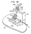
- an integrated circuit region 101A on which various integrated circuits have been constructed is present on a surface of a large-sized semiconductor substrate 101 made of a semiconductor wafer.
- a rectangular opening 102 which has been formed by, for instance, etching treatment, is formed.
- the semiconductor substrate 101 is supported by an upper supporting member 105A and a lower supporting member 105B made of, e.g., an epoxy resin in such a manner that, a rectangular pillar 103 made of, for instance, an alminium alloy or a plastic resin is pierced through the opening 102, and the substrate is sandwiched by both the upper and lower supporting members 105A and 105B formed on the four sides of the pillar 103.
- the central portion of this pillar 103 is made empty.
- a size of the opening 102 of the substrate 101 is defined under the condition that the pillar 103 can be substantially penetrated through the opening 102 while both the upper and lower supporting members 105A and 105B are bent toward the pillar side.
- the pillar 103 is made of a metal such as aluminium, the surface of the metal pillar is covered with a resin so as to electrically insulate the wiring leads.
- a plurality of connector pins 104 are formed on the bottom of the pillar 103 so as to package the pillar 103 which mounts a plurality of semiconductor substrates 101, on a packaging substrate (not shown).
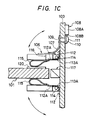
- Both the upper and lower supporting members 105A and 105B have such a shape that, as illustrated in Figs. 1B and 1C, each edge thereof located at the pillar 103 is engaged with a supporting projection 103A which projects from the pillar 103.
- a hole 119 for penetrating a supporting shaft 114 therethrough is formed on the upper supporting member 105A, lower supporting member 105B, and supporting projection 103A, respectively. That is to say, both the upper and lower supporting members 105A and 105B are mounted on the supporting projection 103A in such a manner that they can be rotated with respect to the supporting axis 114 as its rotating center.
- a twist coil spring 112 is arranged on both sides of the upper and lower supporting members 105A and 105B, one end 112A of the twist coil spring 112 is fixed to either the upper supporting member 105A or lower supporting member 105B, and the supporting shaft 114 is penetrated through a central hole 113 thereof. It is seen that only twist coil spring 112 of one edge of the respective upper and lower supporting members 105A and 105B in Figs. 1B and 1C. As a result, the semiconductor substrate 101 is supported by the upper and lower supporting members 105A and 105B by means of the elasticity of the above-described twist coil spring 112.
- a plurality of fixing electrodes are fixed on the upper surface of the upper supporting member 105A, which are made of aluminium on which, for instance, copper or silver is plated.
- a plurality of brush electrodes having elasticity are provided on the side of the pillar 103 corresponding to the fixing electrodes 106, and one end of the respective brush electrodes is resiliently in contact with the surface of the corresponding fixing electrodes 106.
- the end portion of the respective brush electrodes 107 which is resiliently in contact with the respective fixing electrodes, is slidable on the corresponding fixing electrode 106 while the upper supporting members 105A is rotated.
- Another electrode 110 made of, for example, cupper is provided on an inner surface of the pillar 103, in relation to the above-described brush electrode 107, and is connected to the brush electrode 107 by a lead 109 made of, for instance, aluminium on which silver is plated. Between this lead 109 and the pillar 103, an epoxy resin is provided for electrical insulation.
- the insulated cable 108 is attached to the pillar 103 by adhesive agent so that these insulated cables are employed to connect between the respective semiconductor substrates 101 provided on the pillar 103 and also the semiconductor substrate 101 and the connector pin 104 shown in Fig. 1A.
- a spring electrode 115 having elasticity is provided on the upper surface corresponding to the respective fixing electrodes 106 of the upper supporting member 105A.
- a pin 116 made of, for example, silver-plated aluminium is mechanically and electrically connected between the spring electrode and the fixing electrode 106.
- the respective spring electrodes 115 are resiliently in contact with an electrode 120 made of, for example, an aluminium film which is provided on the surface of the semiconductor substrate 101.
- a spring electrode 115 is provided on the lower supporting member 105B in order that it is used as a supporting member for sandwiching the semiconductor substrate 101. That is to say, the semiconductor substrate 101 is supported in such a manner that a plurality of spring electrodes 115 respectively provided on the upper and lower supporting members 105A and 105B sandwich this substrate 101.
- the upper and lower supporting members 105A and 105B are bent toward the pillar by the manual operation.
- a rubber 117 made of, for instance, a sillicone rubber for preventing the horizontal vibrations is employed between the upper supporting member 105A of the pillar 103 and the lower supporting member 105B.
- the pillar 103 may be shaped as a cylinder according to the invention. In this case, it is apparent that the shape of the opening 102 formed on the semiconductor substrate 101 may be circle.
- both rear surfaces of two sheets of the semiconductor substrates 101, on which no integrated circuit 101A is arranged, are connected to each other by the adhesive agent, and thus the connected semiconductor substrates are sandwiched by these upper and lower supporting members 105A and 105B.
- an interval between the upper and lower supporting members 105A and 105B is wider than that of a single semiconductor substrate 105.
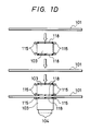
- the packaging device according to the invention may be constructed as packaging device as shown in Fig. 1D.
- the semiconductor substrate 101 has no opening 102 as illustrated in Figs. 1A to 1C.
- the shape of the pillar 103 is formed as a rectanglar pillar or a cylindircal pillar, the upper and lower edges of which are flat surfaces. That is to say, an interior of the pillar 103 is formed as a cavity, and both the upper and lower ends thereof are made closed.
- the adhesive agent 118 is coated on both the upper and lower ends thereof are made closed.
- the adhesive agent 118 is coated on both the upper and lower ends which are in turn attached to the central portion of the semiconductor substrate 101. No integrated circuit is constructed on the portion to which the pillar 103 of the semiconductor substrate 101 is attached.
- Connecting electrodes (not shown) are employed on both surfaces of the semiconductor substrate 101, corresponding to the electrode 115 mounted on the pillar 103. Electrical connection is made between the electrodes formed on both surfaces of the semiconductor substrate 101 via the connecting hole which penetrates through the semiconductor substrate 101.
- the pillar 103 and semiconductor substrate 101 are alternately stacked from the bottom.
- the packaging device for packaging the large-sized semiconductor substrate in a stable condition can be realized.
- reference numeral 203 denotes a semiconductor wafer made of a monocrystal silicon and reference numeral 203A indicates an integrated circuit region for constructing various integrated circuits.
- a packaging device of a semiconductor integrated circuit includes pillars 201a, 201b, 201c and 201d standing at a peripheral portion of an integrated wafer 203, and a pillar connecting substrate 202 which is connected to the lower end portions of these pillars 201a and 201d so as to stably stand these pillars.
- the pillar 201 and pillar connecting substrate 202 are made of a resin such as an epoxy resin, or aluminium.
- the semiconductor wafer 203 is sandwiched by semiconductor substrate supporting members 205 and 210 which are provided on the pillar 201.
- the pillars for instance, 201b and 201c are arranged to be bent, or brought down as shown in Fig. 2E.
- the remaining pillars 201a and 201d are fixed on the pillar connecting substrate 202.
- only the pillar 201a, three pillars 201a to 201c, or all of the pillars 201a to 201d may be bent or brought down.
- the pillars 201 other than the bendable pillars 201 are fixed on the pillar connecting substrate 202.
- the semiconductor wafer 203 is supported by the upper semiconductor substrate supporting member 205 and the lower semiconductor substrate supporting member 206 mounted on the pillar 201 in the fixed condition.
- the upper semiconductor substrate supporting member 210 is made of, for instance, a resin such as an epoxy resin, or alminium, and is integrally formed with, for example, the pillar 201.
- the lower semiconductor substrate supporting member 210 is mounted on a supporting section 201A projecting from the pillar 201 in such a manner that it is rotatable around the supporting shaft 212.
- the lower semiconductor substrate supporting member 210 is made of, for instance, a resin such as a glass epoxy resin, or aluminium.
- a plurality of hair-pin-shaped spring electrodes 206 are provided on the lower surface of the upper semiconductor substrate supporting member 205 so as to be resiliently connected to the electrode 204 of the semiconductor wafer 203.
- the spring electrode 206 is connected via an embeded wiring lead 207 which penetrates through the upper semiconductor substrate supporting member 205, and the upper wiring lead 208 of the upper surface of the upper semiconductor substrate supporting member 205, to a terminal electrode 214 provided on the outer wall of the pillar 201.
- the wiring lead 208 penetrates through a through hole formed on the pillar 201.
- the hair-pin-shaped pressure spring 211 is provided on the upper surface of the lower semiconductor substrate supporting member 210, i.e., the plane opposite to the semiconductor wafer 203.
- a handle 213 is mounted on the lower surface of the lower semiconductor substrate supporting member 210 so as to open a space defined between the upper and lower semiconductor substrate supporting members 205 and 210 when mounting the semiconductor wafer 203.
- the above-described upper semiconductor substrate supporting member 205, lower semiconductor substrate supporting member 210, and coil spring 209 are mounted on the corresponding pillars 201a, 201b, 201c and 201d, so that the semiconductor wafer 203 can be sandwiched at four positions under the stable condition.
- the above-described spring electrode 206, wiring leads 207 and 208, coil spring 209 and pressure spring 211 are mounted on the respective upper and lower substrate supporting members 205 and 210 which are mounted on the corresponding four pillars 201. With respect to the spring electrode 206, the electrode 204 is arranged to the semiconductor wafer 203.
- a core 215A of a cable 215 which is insulating-covered with vinyle chloride is connected by solder.
- This insulating cable 215 connects the respective semiconductor wafers 203, and the semiconductor wafers 203 packaged on the packaging substrate and also the wiring lines on the packaging substrate.
- a sandwiching member of the semiconductor wafer 203 is provided in such a manner that the semiconductor wafer supporting, or sandwiching member 205 is ⁇ -shaped, and both the spring electrode 206 and pressure spring 211 are fixed on the side surface of the inside thereof.
- the pillar 201 defines a cavity 218 of a cylindrical form at the portion corresponding to the semiconductor substrate supporting member 205 in order to fit with the semiconductor substrate supporting member 205.
- the semiconductor substrate supporting member 205 fitted within this cavity 218 is positioned to be depressed by the coil spring 219.
- a terminal electrode 217 is provided on the upper surface of the semiconductor substrate supporting member 205, to which the core 215A of the cable 215 is connected.
- the cable 215 extends over the plane opposite to the semiconductor wafer 203, i.e., the outer wall of the pillar 201. This cable 215 is connected via a through hole formed on the pillar 201 adjacent to the semiconductor substrate supporting member 215 to the terminal electrode 216. To achieve the better connection between the spring electrode 206 and the electrode 204 and also firmly sandwich the semiconductor wafer 203, an interval between the spring electrode 206 and pressure spring 211 by which the semiconductor wafer 203 is not yet mounted, is narrower than the thickness of the semiconductor wafer 203.
- FIG. 2E One example of the connection between the lower end portion of the pillar 201 and the pillar connecting substrate 202 is shown in Fig. 2E.
- the connecting portion of the pillar connecting substrate 202 is engaged with the lower portion of the pillar 201, and rotatably connected in such a manner that a mounting bolt 227 is inserted into the corresponding bolt hole 230 formed on these portions.
- the bolt 227 is so arranged that it is not dropped from the corresponding bolt hole 230 by mounting a nut 228 on the screw section 227.
- a twist coil spring 222 is positioned on both sides of the pillar and the bolt 227 is penetrated through the respective center holes 226.
- this twist coil spring 222 is mounted in the spring mounting hole 223 of the pillar connecting substrate 202, whereas the other end thereof is mounted in the spring mounting hole 225 formed on the projecting 224 of the pillar 201.
- the pillar 201 can be stood up at a right angle by this twist coil spring 222, and also the bent pillar 201 can be recovered by means of the twist coil spring 222.
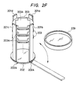
- both the pillar 201 and pillar connecting substrate 202 may be constructed as shown in Fig. 2F.
- pillar 201b among four pillars 201 is so arranged to be bent.
- a hinge is mounted between the bent pillar 201b and the pillar connecting substrate 202 at these connecting sections 202A in such a manner that it is mounted between the outer wall of the pillar 201 and the edge portion of the pillar connecting substrate 202. Since the hinge is mounted to the outer wall of the pillar 201b, the pillar is not bent inside, but allowable to be bent outside.
- a lid 229 is employed to cover it.
- the semiconductor substrate supporting members 205 shown in Fig. 2B or 2C and 210 are provided with the pillar 201 illustrated in Fig. 2F.
- Both the rear surfaces of the semiconductor wafer 203, for instance, are attached to each other, and the resultant semiconductor wafers 203 may be supported by either the semiconductor substrate supporting members 205 and 210 (see Fig. 2B), or 205 (Fig. 2C).
- the interval between the semiconductor supporting members 205, 210, and 205, into which the semiconductor wafer 203 can be inserted is made wider than that of the single semiconductor wafer 203.
- the semiconductor wafer 203 is not limited to the above-mentioned wafer, but may be such a semiconductor substrate that, for example, the peripherals of the semiconductor wafer 203 are cut off to form a rectangle-shaped semiconductor wafer.
- the layout for arranging the respective pillars 201, and the size and shape of the pillar connecting substrate 202 may be modified, depending upon the size and shape of the employed semiconductor substrate.
- the packaging device is constructed of a plurality of pillars standing around the peripherals of the semiconductor wafer, the semiconductor substrate supporting members and pillar connecting members and pillar connecting substrate mounted thereto, the semiconductor wafer can be supported thereon without any twist and vibration phenomenon. As a consequence, a large-sized semiconductor integrated circuit constructed of a semiconductor wafer can be packaged under the stable condition.
Landscapes
- Packaging Frangible Articles (AREA)
- Design And Manufacture Of Integrated Circuits (AREA)
- Semiconductor Memories (AREA)
- Internal Circuitry In Semiconductor Integrated Circuit Devices (AREA)
- Techniques For Improving Reliability Of Storages (AREA)
- Container, Conveyance, Adherence, Positioning, Of Wafer (AREA)
- Testing Or Measuring Of Semiconductors Or The Like (AREA)
Claims (8)
- Stapel groß bemessener Halbleitersubstrate, mit einer Montagevorrichtung mit einer Vielzahl von Eingriffseinrichtungen, wobei jede Eingriffseinrichtung zum Eingriff in jeweils ein einzelnes der Substrate eingerichtet ist, um die Substrate in gegenseitigem Abstand zuhalten, dadurch gekennzeichnet, daß die Eingriffseinrichtung eine Einrichtung zum Herstellen einer Vielzahl unabhängiger elektrischer Anschlüsse an das Substrat umfaßt.
- Stapel nach Anspruch 1, worin die Montagevorrichtung in die Substrate an einem mittigen Teil dieser Substrate eingreift.
- Stapel nach Anspruch 2, worin jedes Substrat eine Öffnung an seinem mittigen Teil aufweist und die Montageeinrichtung eine längliche Säule aufweist, die sich durch diese Öffnungen erstreckt und in jedes Substrat an oder nahe der Öffnung eingreift.
- Stapel nach Anspruch 1, worin die Montagevorrichtung eine Vielzahl miteinander verbundener Säulen aufweist, von denen jede eine Einrichtung zum Eingriff in die Substrate am Umfang dieser Substrate aufweist.
- Stapel nach Anspruch 4, worin die Säulen miteinander durch einen Sockel verbunden sind und die Säulen an diesem Sockel gelenkig angebracht sind.
- Stapel nach Anspruch 5, worin die Säulen am Sockel über eine Feder gelenkig angebracht sind, die die Säulen in Richtung des Eingriffs mit den Substraten belastet.
- Stapel nach irgendeinem der vorangehenden Ansprüche, worin die Montagevorrichtung eine Einrichtung zum Herstellen eines elektrischen Kontakts mit jedem Substrat aufweist.
- Stapel nach Anspruch 7, worin die Einrichtung zum Herstellen eines Kontakts eine Federelektrode ist.
Priority Applications (1)
| Application Number | Priority Date | Filing Date | Title |
|---|---|---|---|
| EP92112517A EP0516185B1 (de) | 1987-04-22 | 1988-04-08 | Integrierte Halbleiterschaltungen Vorrichtung von Scheibengrösse |
Applications Claiming Priority (10)
| Application Number | Priority Date | Filing Date | Title |
|---|---|---|---|
| JP97326/87 | 1987-04-22 | ||
| JP62097326A JPS63263747A (ja) | 1987-04-22 | 1987-04-22 | 実装基板の製造方法 |
| JP97330/87 | 1987-04-22 | ||
| JP62097329A JPS63263736A (ja) | 1987-04-22 | 1987-04-22 | 半導体装置 |
| JP97329/87 | 1987-04-22 | ||
| JP62097331A JPS63263735A (ja) | 1987-04-22 | 1987-04-22 | 半導体集積回路の実装装置 |
| JP97331/87 | 1987-04-22 | ||
| JP62097330A JPS63263734A (ja) | 1987-04-22 | 1987-04-22 | 半導体集積回路の実装装置 |
| JP62099779A JPS63266700A (ja) | 1987-04-24 | 1987-04-24 | ウエハ大半導体集積回路装置 |
| JP99779/87 | 1987-04-24 |
Related Child Applications (1)
| Application Number | Title | Priority Date | Filing Date |
|---|---|---|---|
| EP92112517.5 Division-Into | 1988-04-08 |
Publications (3)
| Publication Number | Publication Date |
|---|---|
| EP0288186A2 EP0288186A2 (de) | 1988-10-26 |
| EP0288186A3 EP0288186A3 (en) | 1990-05-23 |
| EP0288186B1 true EP0288186B1 (de) | 1993-06-30 |
Family
ID=27525857
Family Applications (2)
| Application Number | Title | Priority Date | Filing Date |
|---|---|---|---|
| EP88303160A Expired - Lifetime EP0288186B1 (de) | 1987-04-22 | 1988-04-08 | Verpackung von integrierten Halbleiterschaltungen |
| EP92112517A Expired - Lifetime EP0516185B1 (de) | 1987-04-22 | 1988-04-08 | Integrierte Halbleiterschaltungen Vorrichtung von Scheibengrösse |
Family Applications After (1)
| Application Number | Title | Priority Date | Filing Date |
|---|---|---|---|
| EP92112517A Expired - Lifetime EP0516185B1 (de) | 1987-04-22 | 1988-04-08 | Integrierte Halbleiterschaltungen Vorrichtung von Scheibengrösse |
Country Status (5)
| Country | Link |
|---|---|
| EP (2) | EP0288186B1 (de) |
| KR (2) | KR960012649B1 (de) |
| DE (2) | DE3882074T2 (de) |
| HK (1) | HK28096A (de) |
| SG (1) | SG36588G (de) |
Families Citing this family (5)
| Publication number | Priority date | Publication date | Assignee | Title |
|---|---|---|---|---|
| US5598031A (en) * | 1993-06-23 | 1997-01-28 | Vlsi Technology, Inc. | Electrically and thermally enhanced package using a separate silicon substrate |
| EP0705485A1 (de) * | 1993-06-23 | 1996-04-10 | Vlsi Technology, Inc. | Elektrisch und thermisch verbesserte packung durch benutzung eines separaten siliziumsubstrats |
| KR19980064369A (ko) * | 1996-12-19 | 1998-10-07 | 윌리엄비.켐플러 | 메모리 모듈, 메모리 탑 및 메모리 모듈 구성 방법 |
| JP2001102523A (ja) * | 1999-09-28 | 2001-04-13 | Sony Corp | 薄膜デバイスおよびその製造方法 |
| JP2003229517A (ja) | 2002-01-31 | 2003-08-15 | Fujitsu Hitachi Plasma Display Ltd | 半導体チップ実装基板及びフラットディスプレイ |
Family Cites Families (2)
| Publication number | Priority date | Publication date | Assignee | Title |
|---|---|---|---|---|
| US3908155A (en) * | 1974-04-19 | 1975-09-23 | Ibm | Wafer circuit package |
| DE2611749C3 (de) * | 1976-03-19 | 1980-11-13 | Siemens Ag, 1000 Berlin Und 8000 Muenchen | Halbleiteranordnung mit einem über Spannbolzen durch Druck kontaktierbaren Halbleiterbauelement |
-
1988
- 1988-03-29 KR KR88003425A patent/KR960012649B1/ko not_active Expired - Fee Related
- 1988-04-08 SG SG1995905451A patent/SG36588G/en unknown
- 1988-04-08 DE DE88303160T patent/DE3882074T2/de not_active Expired - Fee Related
- 1988-04-08 EP EP88303160A patent/EP0288186B1/de not_active Expired - Lifetime
- 1988-04-08 DE DE3856019T patent/DE3856019T2/de not_active Expired - Fee Related
- 1988-04-08 EP EP92112517A patent/EP0516185B1/de not_active Expired - Lifetime
-
1993
- 1993-03-18 KR KR93004115A patent/KR970001885B1/ko not_active Expired - Fee Related
-
1996
- 1996-02-15 HK HK28096A patent/HK28096A/xx unknown
Also Published As
| Publication number | Publication date |
|---|---|
| EP0516185A2 (de) | 1992-12-02 |
| HK28096A (en) | 1996-02-23 |
| EP0288186A3 (en) | 1990-05-23 |
| KR930020560A (ko) | 1993-10-20 |
| HK1003348A1 (en) | 1998-10-23 |
| KR960012649B1 (en) | 1996-09-23 |
| DE3856019T2 (de) | 1998-04-02 |
| DE3856019D1 (de) | 1997-10-09 |
| KR880013223A (ko) | 1988-11-30 |
| DE3882074T2 (de) | 1993-10-07 |
| EP0288186A2 (de) | 1988-10-26 |
| KR970001885B1 (en) | 1997-02-18 |
| SG36588G (en) | 1995-09-01 |
| DE3882074D1 (de) | 1993-08-05 |
| EP0516185B1 (de) | 1997-09-03 |
| EP0516185A3 (en) | 1993-03-17 |
Similar Documents
| Publication | Publication Date | Title |
|---|---|---|
| US6078501A (en) | Power semiconductor module | |
| US4225900A (en) | Integrated circuit device package interconnect means | |
| KR100277308B1 (ko) | 반도체장치 | |
| US6344683B1 (en) | Stacked semiconductor package with flexible tape | |
| US6343019B1 (en) | Apparatus and method of stacking die on a substrate | |
| US6175159B1 (en) | Semiconductor package | |
| US4941033A (en) | Semiconductor integrated circuit device | |
| US5933710A (en) | Method of providing electrical connection between an integrated circuit die and a printed circuit board | |
| US5172303A (en) | Electronic component assembly | |
| EP0352429B1 (de) | Automatische Bandmontage-Packung hoher Leistung vom Steckerstift-Typ | |
| US4905124A (en) | IC card | |
| US5422435A (en) | Stacked multi-chip modules and method of manufacturing | |
| JP3226752B2 (ja) | 半導体装置の製造方法 | |
| US5777382A (en) | Plastic packaging for a surface mounted integrated circuit | |
| JP2932432B2 (ja) | 半導体パッケージの構造及びパッケージ方法 | |
| KR20010034154A (ko) | 다수의 기판층과 적어도 하나의 반도체 칩을 가진 반도체소자 및 그의 제조 방법 | |
| EP1429389A1 (de) | Kompaktes Halbleitermodul dass sehr genau montiert werden kann und dessen Herstellungsverfahren | |
| US6987313B2 (en) | Semiconductor device | |
| EP0288186B1 (de) | Verpackung von integrierten Halbleiterschaltungen | |
| US5455741A (en) | Wire-lead through hole interconnect device | |
| JPH04297043A (ja) | 垂直半導体相互接続方法及び構成体 | |
| US3984739A (en) | Structure for packaging integrated circuits | |
| US5734196A (en) | Electronic packaging shaped beam lead fabrication | |
| EP0924845A2 (de) | Leistungshalbleitermodul | |
| EP0282124B1 (de) | Verfahren zum Herstellen einer Modul-Halbleiter-Leistungsanordnung und hergestellte Anordnung |
Legal Events
| Date | Code | Title | Description |
|---|---|---|---|
| PUAI | Public reference made under article 153(3) epc to a published international application that has entered the european phase |
Free format text: ORIGINAL CODE: 0009012 |
|
| AK | Designated contracting states |
Kind code of ref document: A2 Designated state(s): DE FR GB IT |
|
| PUAL | Search report despatched |
Free format text: ORIGINAL CODE: 0009013 |
|
| AK | Designated contracting states |
Kind code of ref document: A3 Designated state(s): DE FR GB IT |
|
| 17P | Request for examination filed |
Effective date: 19900927 |
|
| 17Q | First examination report despatched |
Effective date: 19910919 |
|
| GRAA | (expected) grant |
Free format text: ORIGINAL CODE: 0009210 |
|
| AK | Designated contracting states |
Kind code of ref document: B1 Designated state(s): DE FR GB IT |
|
| XX | Miscellaneous (additional remarks) |
Free format text: TEILANMELDUNG 92112517.5 EINGEREICHT AM 08/04/88. |
|
| REF | Corresponds to: |
Ref document number: 3882074 Country of ref document: DE Date of ref document: 19930805 |
|
| ET | Fr: translation filed | ||
| ITF | It: translation for a ep patent filed | ||
| PLBE | No opposition filed within time limit |
Free format text: ORIGINAL CODE: 0009261 |
|
| STAA | Information on the status of an ep patent application or granted ep patent |
Free format text: STATUS: NO OPPOSITION FILED WITHIN TIME LIMIT |
|
| 26N | No opposition filed | ||
| PGFP | Annual fee paid to national office [announced via postgrant information from national office to epo] |
Ref country code: GB Payment date: 19950329 Year of fee payment: 8 |
|
| PGFP | Annual fee paid to national office [announced via postgrant information from national office to epo] |
Ref country code: FR Payment date: 19950418 Year of fee payment: 8 |
|
| PGFP | Annual fee paid to national office [announced via postgrant information from national office to epo] |
Ref country code: DE Payment date: 19950626 Year of fee payment: 8 |
|
| PG25 | Lapsed in a contracting state [announced via postgrant information from national office to epo] |
Ref country code: GB Effective date: 19960408 |
|
| GBPC | Gb: european patent ceased through non-payment of renewal fee |
Effective date: 19960408 |
|
| PG25 | Lapsed in a contracting state [announced via postgrant information from national office to epo] |
Ref country code: FR Effective date: 19961227 |
|
| PG25 | Lapsed in a contracting state [announced via postgrant information from national office to epo] |
Ref country code: DE Effective date: 19970101 |
|
| REG | Reference to a national code |
Ref country code: FR Ref legal event code: ST |
|
| PG25 | Lapsed in a contracting state [announced via postgrant information from national office to epo] |
Ref country code: IT Free format text: LAPSE BECAUSE OF NON-PAYMENT OF DUE FEES;WARNING: LAPSES OF ITALIAN PATENTS WITH EFFECTIVE DATE BEFORE 2007 MAY HAVE OCCURRED AT ANY TIME BEFORE 2007. THE CORRECT EFFECTIVE DATE MAY BE DIFFERENT FROM THE ONE RECORDED. Effective date: 20050408 |