EP0288186B1 - Packaging of semiconductor integrated circuits - Google Patents
Packaging of semiconductor integrated circuits Download PDFInfo
- Publication number
- EP0288186B1 EP0288186B1 EP88303160A EP88303160A EP0288186B1 EP 0288186 B1 EP0288186 B1 EP 0288186B1 EP 88303160 A EP88303160 A EP 88303160A EP 88303160 A EP88303160 A EP 88303160A EP 0288186 B1 EP0288186 B1 EP 0288186B1
- Authority
- EP
- European Patent Office
- Prior art keywords
- pillar
- semiconductor
- substrate
- semiconductor substrate
- substrates
- Prior art date
- Legal status (The legal status is an assumption and is not a legal conclusion. Google has not performed a legal analysis and makes no representation as to the accuracy of the status listed.)
- Expired - Lifetime
Links
Images


Classifications
-
- H—ELECTRICITY
- H01—ELECTRIC ELEMENTS
- H01L—SEMICONDUCTOR DEVICES NOT COVERED BY CLASS H10
- H01L23/00—Details of semiconductor or other solid state devices
- H01L23/52—Arrangements for conducting electric current within the device in operation from one component to another, i.e. interconnections, e.g. wires, lead frames
- H01L23/538—Arrangements for conducting electric current within the device in operation from one component to another, i.e. interconnections, e.g. wires, lead frames the interconnection structure between a plurality of semiconductor chips being formed on, or in, insulating substrates
- H01L23/5385—Assembly of a plurality of insulating substrates
-
- H—ELECTRICITY
- H01—ELECTRIC ELEMENTS
- H01L—SEMICONDUCTOR DEVICES NOT COVERED BY CLASS H10
- H01L23/00—Details of semiconductor or other solid state devices
- H01L23/12—Mountings, e.g. non-detachable insulating substrates
-
- H—ELECTRICITY
- H01—ELECTRIC ELEMENTS
- H01L—SEMICONDUCTOR DEVICES NOT COVERED BY CLASS H10
- H01L23/00—Details of semiconductor or other solid state devices
- H01L23/12—Mountings, e.g. non-detachable insulating substrates
- H01L23/14—Mountings, e.g. non-detachable insulating substrates characterised by the material or its electrical properties
- H01L23/147—Semiconductor insulating substrates
-
- H—ELECTRICITY
- H01—ELECTRIC ELEMENTS
- H01L—SEMICONDUCTOR DEVICES NOT COVERED BY CLASS H10
- H01L23/00—Details of semiconductor or other solid state devices
- H01L23/32—Holders for supporting the complete device in operation, i.e. detachable fixtures
-
- H—ELECTRICITY
- H01—ELECTRIC ELEMENTS
- H01L—SEMICONDUCTOR DEVICES NOT COVERED BY CLASS H10
- H01L25/00—Assemblies consisting of a plurality of individual semiconductor or other solid state devices ; Multistep manufacturing processes thereof
- H01L25/03—Assemblies consisting of a plurality of individual semiconductor or other solid state devices ; Multistep manufacturing processes thereof all the devices being of a type provided for in the same subgroup of groups H01L27/00 - H01L33/00, or in a single subclass of H10K, H10N, e.g. assemblies of rectifier diodes
- H01L25/04—Assemblies consisting of a plurality of individual semiconductor or other solid state devices ; Multistep manufacturing processes thereof all the devices being of a type provided for in the same subgroup of groups H01L27/00 - H01L33/00, or in a single subclass of H10K, H10N, e.g. assemblies of rectifier diodes the devices not having separate containers
- H01L25/065—Assemblies consisting of a plurality of individual semiconductor or other solid state devices ; Multistep manufacturing processes thereof all the devices being of a type provided for in the same subgroup of groups H01L27/00 - H01L33/00, or in a single subclass of H10K, H10N, e.g. assemblies of rectifier diodes the devices not having separate containers the devices being of a type provided for in group H01L27/00
- H01L25/0652—Assemblies consisting of a plurality of individual semiconductor or other solid state devices ; Multistep manufacturing processes thereof all the devices being of a type provided for in the same subgroup of groups H01L27/00 - H01L33/00, or in a single subclass of H10K, H10N, e.g. assemblies of rectifier diodes the devices not having separate containers the devices being of a type provided for in group H01L27/00 the devices being arranged next and on each other, i.e. mixed assemblies
-
- H—ELECTRICITY
- H01—ELECTRIC ELEMENTS
- H01L—SEMICONDUCTOR DEVICES NOT COVERED BY CLASS H10
- H01L25/00—Assemblies consisting of a plurality of individual semiconductor or other solid state devices ; Multistep manufacturing processes thereof
- H01L25/03—Assemblies consisting of a plurality of individual semiconductor or other solid state devices ; Multistep manufacturing processes thereof all the devices being of a type provided for in the same subgroup of groups H01L27/00 - H01L33/00, or in a single subclass of H10K, H10N, e.g. assemblies of rectifier diodes
- H01L25/04—Assemblies consisting of a plurality of individual semiconductor or other solid state devices ; Multistep manufacturing processes thereof all the devices being of a type provided for in the same subgroup of groups H01L27/00 - H01L33/00, or in a single subclass of H10K, H10N, e.g. assemblies of rectifier diodes the devices not having separate containers
- H01L25/07—Assemblies consisting of a plurality of individual semiconductor or other solid state devices ; Multistep manufacturing processes thereof all the devices being of a type provided for in the same subgroup of groups H01L27/00 - H01L33/00, or in a single subclass of H10K, H10N, e.g. assemblies of rectifier diodes the devices not having separate containers the devices being of a type provided for in group H01L29/00
- H01L25/073—Apertured devices mounted on one or more rods passed through the apertures
-
- H—ELECTRICITY
- H01—ELECTRIC ELEMENTS
- H01L—SEMICONDUCTOR DEVICES NOT COVERED BY CLASS H10
- H01L2224/00—Indexing scheme for arrangements for connecting or disconnecting semiconductor or solid-state bodies and methods related thereto as covered by H01L24/00
- H01L2224/01—Means for bonding being attached to, or being formed on, the surface to be connected, e.g. chip-to-package, die-attach, "first-level" interconnects; Manufacturing methods related thereto
- H01L2224/02—Bonding areas; Manufacturing methods related thereto
- H01L2224/04—Structure, shape, material or disposition of the bonding areas prior to the connecting process
- H01L2224/0401—Bonding areas specifically adapted for bump connectors, e.g. under bump metallisation [UBM]
-
- H—ELECTRICITY
- H01—ELECTRIC ELEMENTS
- H01L—SEMICONDUCTOR DEVICES NOT COVERED BY CLASS H10
- H01L2224/00—Indexing scheme for arrangements for connecting or disconnecting semiconductor or solid-state bodies and methods related thereto as covered by H01L24/00
- H01L2224/01—Means for bonding being attached to, or being formed on, the surface to be connected, e.g. chip-to-package, die-attach, "first-level" interconnects; Manufacturing methods related thereto
- H01L2224/02—Bonding areas; Manufacturing methods related thereto
- H01L2224/04—Structure, shape, material or disposition of the bonding areas prior to the connecting process
- H01L2224/05—Structure, shape, material or disposition of the bonding areas prior to the connecting process of an individual bonding area
- H01L2224/0554—External layer
- H01L2224/05599—Material
-
- H—ELECTRICITY
- H01—ELECTRIC ELEMENTS
- H01L—SEMICONDUCTOR DEVICES NOT COVERED BY CLASS H10
- H01L2224/00—Indexing scheme for arrangements for connecting or disconnecting semiconductor or solid-state bodies and methods related thereto as covered by H01L24/00
- H01L2224/01—Means for bonding being attached to, or being formed on, the surface to be connected, e.g. chip-to-package, die-attach, "first-level" interconnects; Manufacturing methods related thereto
- H01L2224/10—Bump connectors; Manufacturing methods related thereto
- H01L2224/15—Structure, shape, material or disposition of the bump connectors after the connecting process
- H01L2224/16—Structure, shape, material or disposition of the bump connectors after the connecting process of an individual bump connector
- H01L2224/161—Disposition
- H01L2224/16151—Disposition the bump connector connecting between a semiconductor or solid-state body and an item not being a semiconductor or solid-state body, e.g. chip-to-substrate, chip-to-passive
- H01L2224/16221—Disposition the bump connector connecting between a semiconductor or solid-state body and an item not being a semiconductor or solid-state body, e.g. chip-to-substrate, chip-to-passive the body and the item being stacked
- H01L2224/16225—Disposition the bump connector connecting between a semiconductor or solid-state body and an item not being a semiconductor or solid-state body, e.g. chip-to-substrate, chip-to-passive the body and the item being stacked the item being non-metallic, e.g. insulating substrate with or without metallisation
-
- H—ELECTRICITY
- H01—ELECTRIC ELEMENTS
- H01L—SEMICONDUCTOR DEVICES NOT COVERED BY CLASS H10
- H01L2224/00—Indexing scheme for arrangements for connecting or disconnecting semiconductor or solid-state bodies and methods related thereto as covered by H01L24/00
- H01L2224/01—Means for bonding being attached to, or being formed on, the surface to be connected, e.g. chip-to-package, die-attach, "first-level" interconnects; Manufacturing methods related thereto
- H01L2224/26—Layer connectors, e.g. plate connectors, solder or adhesive layers; Manufacturing methods related thereto
- H01L2224/31—Structure, shape, material or disposition of the layer connectors after the connecting process
- H01L2224/32—Structure, shape, material or disposition of the layer connectors after the connecting process of an individual layer connector
- H01L2224/321—Disposition
- H01L2224/32151—Disposition the layer connector connecting between a semiconductor or solid-state body and an item not being a semiconductor or solid-state body, e.g. chip-to-substrate, chip-to-passive
- H01L2224/32221—Disposition the layer connector connecting between a semiconductor or solid-state body and an item not being a semiconductor or solid-state body, e.g. chip-to-substrate, chip-to-passive the body and the item being stacked
- H01L2224/32225—Disposition the layer connector connecting between a semiconductor or solid-state body and an item not being a semiconductor or solid-state body, e.g. chip-to-substrate, chip-to-passive the body and the item being stacked the item being non-metallic, e.g. insulating substrate with or without metallisation
-
- H—ELECTRICITY
- H01—ELECTRIC ELEMENTS
- H01L—SEMICONDUCTOR DEVICES NOT COVERED BY CLASS H10
- H01L2224/00—Indexing scheme for arrangements for connecting or disconnecting semiconductor or solid-state bodies and methods related thereto as covered by H01L24/00
- H01L2224/01—Means for bonding being attached to, or being formed on, the surface to be connected, e.g. chip-to-package, die-attach, "first-level" interconnects; Manufacturing methods related thereto
- H01L2224/42—Wire connectors; Manufacturing methods related thereto
- H01L2224/44—Structure, shape, material or disposition of the wire connectors prior to the connecting process
- H01L2224/45—Structure, shape, material or disposition of the wire connectors prior to the connecting process of an individual wire connector
- H01L2224/45001—Core members of the connector
- H01L2224/45099—Material
- H01L2224/451—Material with a principal constituent of the material being a metal or a metalloid, e.g. boron (B), silicon (Si), germanium (Ge), arsenic (As), antimony (Sb), tellurium (Te) and polonium (Po), and alloys thereof
- H01L2224/45117—Material with a principal constituent of the material being a metal or a metalloid, e.g. boron (B), silicon (Si), germanium (Ge), arsenic (As), antimony (Sb), tellurium (Te) and polonium (Po), and alloys thereof the principal constituent melting at a temperature of greater than or equal to 400°C and less than 950°C
- H01L2224/45124—Aluminium (Al) as principal constituent
-
- H—ELECTRICITY
- H01—ELECTRIC ELEMENTS
- H01L—SEMICONDUCTOR DEVICES NOT COVERED BY CLASS H10
- H01L2224/00—Indexing scheme for arrangements for connecting or disconnecting semiconductor or solid-state bodies and methods related thereto as covered by H01L24/00
- H01L2224/01—Means for bonding being attached to, or being formed on, the surface to be connected, e.g. chip-to-package, die-attach, "first-level" interconnects; Manufacturing methods related thereto
- H01L2224/42—Wire connectors; Manufacturing methods related thereto
- H01L2224/44—Structure, shape, material or disposition of the wire connectors prior to the connecting process
- H01L2224/45—Structure, shape, material or disposition of the wire connectors prior to the connecting process of an individual wire connector
- H01L2224/45001—Core members of the connector
- H01L2224/45099—Material
- H01L2224/451—Material with a principal constituent of the material being a metal or a metalloid, e.g. boron (B), silicon (Si), germanium (Ge), arsenic (As), antimony (Sb), tellurium (Te) and polonium (Po), and alloys thereof
- H01L2224/45138—Material with a principal constituent of the material being a metal or a metalloid, e.g. boron (B), silicon (Si), germanium (Ge), arsenic (As), antimony (Sb), tellurium (Te) and polonium (Po), and alloys thereof the principal constituent melting at a temperature of greater than or equal to 950°C and less than 1550°C
- H01L2224/45139—Silver (Ag) as principal constituent
-
- H—ELECTRICITY
- H01—ELECTRIC ELEMENTS
- H01L—SEMICONDUCTOR DEVICES NOT COVERED BY CLASS H10
- H01L2224/00—Indexing scheme for arrangements for connecting or disconnecting semiconductor or solid-state bodies and methods related thereto as covered by H01L24/00
- H01L2224/01—Means for bonding being attached to, or being formed on, the surface to be connected, e.g. chip-to-package, die-attach, "first-level" interconnects; Manufacturing methods related thereto
- H01L2224/42—Wire connectors; Manufacturing methods related thereto
- H01L2224/44—Structure, shape, material or disposition of the wire connectors prior to the connecting process
- H01L2224/45—Structure, shape, material or disposition of the wire connectors prior to the connecting process of an individual wire connector
- H01L2224/45001—Core members of the connector
- H01L2224/45099—Material
- H01L2224/451—Material with a principal constituent of the material being a metal or a metalloid, e.g. boron (B), silicon (Si), germanium (Ge), arsenic (As), antimony (Sb), tellurium (Te) and polonium (Po), and alloys thereof
- H01L2224/45138—Material with a principal constituent of the material being a metal or a metalloid, e.g. boron (B), silicon (Si), germanium (Ge), arsenic (As), antimony (Sb), tellurium (Te) and polonium (Po), and alloys thereof the principal constituent melting at a temperature of greater than or equal to 950°C and less than 1550°C
- H01L2224/45144—Gold (Au) as principal constituent
-
- H—ELECTRICITY
- H01—ELECTRIC ELEMENTS
- H01L—SEMICONDUCTOR DEVICES NOT COVERED BY CLASS H10
- H01L2224/00—Indexing scheme for arrangements for connecting or disconnecting semiconductor or solid-state bodies and methods related thereto as covered by H01L24/00
- H01L2224/01—Means for bonding being attached to, or being formed on, the surface to be connected, e.g. chip-to-package, die-attach, "first-level" interconnects; Manufacturing methods related thereto
- H01L2224/42—Wire connectors; Manufacturing methods related thereto
- H01L2224/47—Structure, shape, material or disposition of the wire connectors after the connecting process
- H01L2224/48—Structure, shape, material or disposition of the wire connectors after the connecting process of an individual wire connector
- H01L2224/4805—Shape
- H01L2224/4809—Loop shape
- H01L2224/48091—Arched
-
- H—ELECTRICITY
- H01—ELECTRIC ELEMENTS
- H01L—SEMICONDUCTOR DEVICES NOT COVERED BY CLASS H10
- H01L2224/00—Indexing scheme for arrangements for connecting or disconnecting semiconductor or solid-state bodies and methods related thereto as covered by H01L24/00
- H01L2224/01—Means for bonding being attached to, or being formed on, the surface to be connected, e.g. chip-to-package, die-attach, "first-level" interconnects; Manufacturing methods related thereto
- H01L2224/42—Wire connectors; Manufacturing methods related thereto
- H01L2224/47—Structure, shape, material or disposition of the wire connectors after the connecting process
- H01L2224/48—Structure, shape, material or disposition of the wire connectors after the connecting process of an individual wire connector
- H01L2224/484—Connecting portions
- H01L2224/48463—Connecting portions the connecting portion on the bonding area of the semiconductor or solid-state body being a ball bond
- H01L2224/48464—Connecting portions the connecting portion on the bonding area of the semiconductor or solid-state body being a ball bond the other connecting portion not on the bonding area also being a ball bond, i.e. ball-to-ball
-
- H—ELECTRICITY
- H01—ELECTRIC ELEMENTS
- H01L—SEMICONDUCTOR DEVICES NOT COVERED BY CLASS H10
- H01L2224/00—Indexing scheme for arrangements for connecting or disconnecting semiconductor or solid-state bodies and methods related thereto as covered by H01L24/00
- H01L2224/01—Means for bonding being attached to, or being formed on, the surface to be connected, e.g. chip-to-package, die-attach, "first-level" interconnects; Manufacturing methods related thereto
- H01L2224/42—Wire connectors; Manufacturing methods related thereto
- H01L2224/47—Structure, shape, material or disposition of the wire connectors after the connecting process
- H01L2224/48—Structure, shape, material or disposition of the wire connectors after the connecting process of an individual wire connector
- H01L2224/484—Connecting portions
- H01L2224/48475—Connecting portions connected to auxiliary connecting means on the bonding areas, e.g. pre-ball, wedge-on-ball, ball-on-ball
- H01L2224/48476—Connecting portions connected to auxiliary connecting means on the bonding areas, e.g. pre-ball, wedge-on-ball, ball-on-ball between the wire connector and the bonding area
- H01L2224/48477—Connecting portions connected to auxiliary connecting means on the bonding areas, e.g. pre-ball, wedge-on-ball, ball-on-ball between the wire connector and the bonding area being a pre-ball (i.e. a ball formed by capillary bonding)
- H01L2224/48484—Connecting portions connected to auxiliary connecting means on the bonding areas, e.g. pre-ball, wedge-on-ball, ball-on-ball between the wire connector and the bonding area being a pre-ball (i.e. a ball formed by capillary bonding) being a plurality of pre-balls disposed side-to-side
-
- H—ELECTRICITY
- H01—ELECTRIC ELEMENTS
- H01L—SEMICONDUCTOR DEVICES NOT COVERED BY CLASS H10
- H01L2224/00—Indexing scheme for arrangements for connecting or disconnecting semiconductor or solid-state bodies and methods related thereto as covered by H01L24/00
- H01L2224/01—Means for bonding being attached to, or being formed on, the surface to be connected, e.g. chip-to-package, die-attach, "first-level" interconnects; Manufacturing methods related thereto
- H01L2224/42—Wire connectors; Manufacturing methods related thereto
- H01L2224/47—Structure, shape, material or disposition of the wire connectors after the connecting process
- H01L2224/48—Structure, shape, material or disposition of the wire connectors after the connecting process of an individual wire connector
- H01L2224/485—Material
- H01L2224/48505—Material at the bonding interface
- H01L2224/48599—Principal constituent of the connecting portion of the wire connector being Gold (Au)
-
- H—ELECTRICITY
- H01—ELECTRIC ELEMENTS
- H01L—SEMICONDUCTOR DEVICES NOT COVERED BY CLASS H10
- H01L2224/00—Indexing scheme for arrangements for connecting or disconnecting semiconductor or solid-state bodies and methods related thereto as covered by H01L24/00
- H01L2224/01—Means for bonding being attached to, or being formed on, the surface to be connected, e.g. chip-to-package, die-attach, "first-level" interconnects; Manufacturing methods related thereto
- H01L2224/42—Wire connectors; Manufacturing methods related thereto
- H01L2224/47—Structure, shape, material or disposition of the wire connectors after the connecting process
- H01L2224/48—Structure, shape, material or disposition of the wire connectors after the connecting process of an individual wire connector
- H01L2224/485—Material
- H01L2224/48505—Material at the bonding interface
- H01L2224/48699—Principal constituent of the connecting portion of the wire connector being Aluminium (Al)
-
- H—ELECTRICITY
- H01—ELECTRIC ELEMENTS
- H01L—SEMICONDUCTOR DEVICES NOT COVERED BY CLASS H10
- H01L2224/00—Indexing scheme for arrangements for connecting or disconnecting semiconductor or solid-state bodies and methods related thereto as covered by H01L24/00
- H01L2224/73—Means for bonding being of different types provided for in two or more of groups H01L2224/10, H01L2224/18, H01L2224/26, H01L2224/34, H01L2224/42, H01L2224/50, H01L2224/63, H01L2224/71
- H01L2224/732—Location after the connecting process
- H01L2224/73251—Location after the connecting process on different surfaces
- H01L2224/73265—Layer and wire connectors
-
- H—ELECTRICITY
- H01—ELECTRIC ELEMENTS
- H01L—SEMICONDUCTOR DEVICES NOT COVERED BY CLASS H10
- H01L24/00—Arrangements for connecting or disconnecting semiconductor or solid-state bodies; Methods or apparatus related thereto
- H01L24/01—Means for bonding being attached to, or being formed on, the surface to be connected, e.g. chip-to-package, die-attach, "first-level" interconnects; Manufacturing methods related thereto
- H01L24/42—Wire connectors; Manufacturing methods related thereto
- H01L24/44—Structure, shape, material or disposition of the wire connectors prior to the connecting process
- H01L24/45—Structure, shape, material or disposition of the wire connectors prior to the connecting process of an individual wire connector
-
- H—ELECTRICITY
- H01—ELECTRIC ELEMENTS
- H01L—SEMICONDUCTOR DEVICES NOT COVERED BY CLASS H10
- H01L24/00—Arrangements for connecting or disconnecting semiconductor or solid-state bodies; Methods or apparatus related thereto
- H01L24/01—Means for bonding being attached to, or being formed on, the surface to be connected, e.g. chip-to-package, die-attach, "first-level" interconnects; Manufacturing methods related thereto
- H01L24/42—Wire connectors; Manufacturing methods related thereto
- H01L24/47—Structure, shape, material or disposition of the wire connectors after the connecting process
- H01L24/48—Structure, shape, material or disposition of the wire connectors after the connecting process of an individual wire connector
-
- H—ELECTRICITY
- H01—ELECTRIC ELEMENTS
- H01L—SEMICONDUCTOR DEVICES NOT COVERED BY CLASS H10
- H01L2924/00—Indexing scheme for arrangements or methods for connecting or disconnecting semiconductor or solid-state bodies as covered by H01L24/00
- H01L2924/0001—Technical content checked by a classifier
- H01L2924/00014—Technical content checked by a classifier the subject-matter covered by the group, the symbol of which is combined with the symbol of this group, being disclosed without further technical details
-
- H—ELECTRICITY
- H01—ELECTRIC ELEMENTS
- H01L—SEMICONDUCTOR DEVICES NOT COVERED BY CLASS H10
- H01L2924/00—Indexing scheme for arrangements or methods for connecting or disconnecting semiconductor or solid-state bodies as covered by H01L24/00
- H01L2924/01—Chemical elements
- H01L2924/01013—Aluminum [Al]
-
- H—ELECTRICITY
- H01—ELECTRIC ELEMENTS
- H01L—SEMICONDUCTOR DEVICES NOT COVERED BY CLASS H10
- H01L2924/00—Indexing scheme for arrangements or methods for connecting or disconnecting semiconductor or solid-state bodies as covered by H01L24/00
- H01L2924/01—Chemical elements
- H01L2924/01014—Silicon [Si]
-
- H—ELECTRICITY
- H01—ELECTRIC ELEMENTS
- H01L—SEMICONDUCTOR DEVICES NOT COVERED BY CLASS H10
- H01L2924/00—Indexing scheme for arrangements or methods for connecting or disconnecting semiconductor or solid-state bodies as covered by H01L24/00
- H01L2924/01—Chemical elements
- H01L2924/01039—Yttrium [Y]
-
- H—ELECTRICITY
- H01—ELECTRIC ELEMENTS
- H01L—SEMICONDUCTOR DEVICES NOT COVERED BY CLASS H10
- H01L2924/00—Indexing scheme for arrangements or methods for connecting or disconnecting semiconductor or solid-state bodies as covered by H01L24/00
- H01L2924/01—Chemical elements
- H01L2924/01079—Gold [Au]
-
- H—ELECTRICITY
- H01—ELECTRIC ELEMENTS
- H01L—SEMICONDUCTOR DEVICES NOT COVERED BY CLASS H10
- H01L2924/00—Indexing scheme for arrangements or methods for connecting or disconnecting semiconductor or solid-state bodies as covered by H01L24/00
- H01L2924/10—Details of semiconductor or other solid state devices to be connected
- H01L2924/102—Material of the semiconductor or solid state bodies
- H01L2924/1025—Semiconducting materials
- H01L2924/10251—Elemental semiconductors, i.e. Group IV
- H01L2924/10253—Silicon [Si]
-
- H—ELECTRICITY
- H01—ELECTRIC ELEMENTS
- H01L—SEMICONDUCTOR DEVICES NOT COVERED BY CLASS H10
- H01L2924/00—Indexing scheme for arrangements or methods for connecting or disconnecting semiconductor or solid-state bodies as covered by H01L24/00
- H01L2924/10—Details of semiconductor or other solid state devices to be connected
- H01L2924/11—Device type
- H01L2924/12—Passive devices, e.g. 2 terminal devices
- H01L2924/1204—Optical Diode
- H01L2924/12042—LASER
-
- H—ELECTRICITY
- H01—ELECTRIC ELEMENTS
- H01L—SEMICONDUCTOR DEVICES NOT COVERED BY CLASS H10
- H01L2924/00—Indexing scheme for arrangements or methods for connecting or disconnecting semiconductor or solid-state bodies as covered by H01L24/00
- H01L2924/10—Details of semiconductor or other solid state devices to be connected
- H01L2924/11—Device type
- H01L2924/13—Discrete devices, e.g. 3 terminal devices
- H01L2924/1304—Transistor
- H01L2924/1305—Bipolar Junction Transistor [BJT]
-
- H—ELECTRICITY
- H01—ELECTRIC ELEMENTS
- H01L—SEMICONDUCTOR DEVICES NOT COVERED BY CLASS H10
- H01L2924/00—Indexing scheme for arrangements or methods for connecting or disconnecting semiconductor or solid-state bodies as covered by H01L24/00
- H01L2924/10—Details of semiconductor or other solid state devices to be connected
- H01L2924/11—Device type
- H01L2924/14—Integrated circuits
-
- H—ELECTRICITY
- H01—ELECTRIC ELEMENTS
- H01L—SEMICONDUCTOR DEVICES NOT COVERED BY CLASS H10
- H01L2924/00—Indexing scheme for arrangements or methods for connecting or disconnecting semiconductor or solid-state bodies as covered by H01L24/00
- H01L2924/15—Details of package parts other than the semiconductor or other solid state devices to be connected
- H01L2924/161—Cap
- H01L2924/1615—Shape
- H01L2924/16152—Cap comprising a cavity for hosting the device, e.g. U-shaped cap
-
- H—ELECTRICITY
- H01—ELECTRIC ELEMENTS
- H01L—SEMICONDUCTOR DEVICES NOT COVERED BY CLASS H10
- H01L2924/00—Indexing scheme for arrangements or methods for connecting or disconnecting semiconductor or solid-state bodies as covered by H01L24/00
- H01L2924/30—Technical effects
- H01L2924/301—Electrical effects
- H01L2924/3025—Electromagnetic shielding
Definitions
- the present invention relates to the packaging of semiconductor integrated circuits according to claim 1, and more particularly to a packaging technique for semiconductor integrated circuits formed on a large-sized semiconductor substrate such as a semiconductor wafer.
- semiconductor integrated circuits are constructed on respective parts of a substate, i.e. a semiconductor wafer chip the wafer then being subdivided by dicing it into a plurality of parts each corresponding to one or more integrated circuits.
- constructions have been investigated in which the semiconductor wafer is not subdivided, but a plurality of integrated circuits are fabricated on the whole of the semiconductor wafer so as to construct a large-sized semiconductor integrated circuit.
- Such a semiconductor manufacturing technique is described in e.g. JP-A-61/290739, in which one large-sized semiconductor integrated circuit is constructed on the entire semiconductor wafer.
- US-A-3 908 155 discloses a device for packaging a stack of wafers interconnected by a common interconnection bus.
- the present invention therefore proposes a stack of large sized semiconductor substrates, comprising a packaging device with a plurality of engaging means, each engaging means being for engaging a respective one of the substrates to maintain the substrates in spaced apart relationship, characterised in that: the engaging means including means for providing a plurality of independent electrical connections to the substrate.
- the engaging means may be a plurality of interconnected pillars each having means for engaging the substrates at the periphery of those substrates. This has the advantage that the wafer(s) are supported at a plurality of positions, so that the wafer(s) cannot vibrate or twist.
- the pillars may then be hingedly interconnected to the base, possibly via springs which holds them into engagement with the wafers.
- the present invention may provide a stack of large-sized semiconductor substrates, comprising a packaging device engaging the substrates to maintain them in a spaced apart relationship.
- the wafer(s) may then be electrically connected to the packaging device, e.g. by spring electrodes.
- an integrated circuit region 101A on which various integrated circuits have been constructed is present on a surface of a large-sized semiconductor substrate 101 made of a semiconductor wafer.
- a rectangular opening 102 which has been formed by, for instance, etching treatment, is formed.
- the semiconductor substrate 101 is supported by an upper supporting member 105A and a lower supporting member 105B made of, e.g., an epoxy resin in such a manner that, a rectangular pillar 103 made of, for instance, an alminium alloy or a plastic resin is pierced through the opening 102, and the substrate is sandwiched by both the upper and lower supporting members 105A and 105B formed on the four sides of the pillar 103.
- the central portion of this pillar 103 is made empty.
- a size of the opening 102 of the substrate 101 is defined under the condition that the pillar 103 can be substantially penetrated through the opening 102 while both the upper and lower supporting members 105A and 105B are bent toward the pillar side.
- the pillar 103 is made of a metal such as aluminium, the surface of the metal pillar is covered with a resin so as to electrically insulate the wiring leads.
- a plurality of connector pins 104 are formed on the bottom of the pillar 103 so as to package the pillar 103 which mounts a plurality of semiconductor substrates 101, on a packaging substrate (not shown).
- Both the upper and lower supporting members 105A and 105B have such a shape that, as illustrated in Figs. 1B and 1C, each edge thereof located at the pillar 103 is engaged with a supporting projection 103A which projects from the pillar 103.
- a hole 119 for penetrating a supporting shaft 114 therethrough is formed on the upper supporting member 105A, lower supporting member 105B, and supporting projection 103A, respectively. That is to say, both the upper and lower supporting members 105A and 105B are mounted on the supporting projection 103A in such a manner that they can be rotated with respect to the supporting axis 114 as its rotating center.
- a twist coil spring 112 is arranged on both sides of the upper and lower supporting members 105A and 105B, one end 112A of the twist coil spring 112 is fixed to either the upper supporting member 105A or lower supporting member 105B, and the supporting shaft 114 is penetrated through a central hole 113 thereof. It is seen that only twist coil spring 112 of one edge of the respective upper and lower supporting members 105A and 105B in Figs. 1B and 1C. As a result, the semiconductor substrate 101 is supported by the upper and lower supporting members 105A and 105B by means of the elasticity of the above-described twist coil spring 112.
- a plurality of fixing electrodes are fixed on the upper surface of the upper supporting member 105A, which are made of aluminium on which, for instance, copper or silver is plated.
- a plurality of brush electrodes having elasticity are provided on the side of the pillar 103 corresponding to the fixing electrodes 106, and one end of the respective brush electrodes is resiliently in contact with the surface of the corresponding fixing electrodes 106.
- the end portion of the respective brush electrodes 107 which is resiliently in contact with the respective fixing electrodes, is slidable on the corresponding fixing electrode 106 while the upper supporting members 105A is rotated.
- Another electrode 110 made of, for example, cupper is provided on an inner surface of the pillar 103, in relation to the above-described brush electrode 107, and is connected to the brush electrode 107 by a lead 109 made of, for instance, aluminium on which silver is plated. Between this lead 109 and the pillar 103, an epoxy resin is provided for electrical insulation.
- the insulated cable 108 is attached to the pillar 103 by adhesive agent so that these insulated cables are employed to connect between the respective semiconductor substrates 101 provided on the pillar 103 and also the semiconductor substrate 101 and the connector pin 104 shown in Fig. 1A.
- a spring electrode 115 having elasticity is provided on the upper surface corresponding to the respective fixing electrodes 106 of the upper supporting member 105A.
- a pin 116 made of, for example, silver-plated aluminium is mechanically and electrically connected between the spring electrode and the fixing electrode 106.
- the respective spring electrodes 115 are resiliently in contact with an electrode 120 made of, for example, an aluminium film which is provided on the surface of the semiconductor substrate 101.
- a spring electrode 115 is provided on the lower supporting member 105B in order that it is used as a supporting member for sandwiching the semiconductor substrate 101. That is to say, the semiconductor substrate 101 is supported in such a manner that a plurality of spring electrodes 115 respectively provided on the upper and lower supporting members 105A and 105B sandwich this substrate 101.
- the upper and lower supporting members 105A and 105B are bent toward the pillar by the manual operation.
- a rubber 117 made of, for instance, a sillicone rubber for preventing the horizontal vibrations is employed between the upper supporting member 105A of the pillar 103 and the lower supporting member 105B.
- the pillar 103 may be shaped as a cylinder according to the invention. In this case, it is apparent that the shape of the opening 102 formed on the semiconductor substrate 101 may be circle.
- both rear surfaces of two sheets of the semiconductor substrates 101, on which no integrated circuit 101A is arranged, are connected to each other by the adhesive agent, and thus the connected semiconductor substrates are sandwiched by these upper and lower supporting members 105A and 105B.
- an interval between the upper and lower supporting members 105A and 105B is wider than that of a single semiconductor substrate 105.
- the packaging device according to the invention may be constructed as packaging device as shown in Fig. 1D.
- the semiconductor substrate 101 has no opening 102 as illustrated in Figs. 1A to 1C.
- the shape of the pillar 103 is formed as a rectanglar pillar or a cylindircal pillar, the upper and lower edges of which are flat surfaces. That is to say, an interior of the pillar 103 is formed as a cavity, and both the upper and lower ends thereof are made closed.
- the adhesive agent 118 is coated on both the upper and lower ends thereof are made closed.
- the adhesive agent 118 is coated on both the upper and lower ends which are in turn attached to the central portion of the semiconductor substrate 101. No integrated circuit is constructed on the portion to which the pillar 103 of the semiconductor substrate 101 is attached.
- Connecting electrodes (not shown) are employed on both surfaces of the semiconductor substrate 101, corresponding to the electrode 115 mounted on the pillar 103. Electrical connection is made between the electrodes formed on both surfaces of the semiconductor substrate 101 via the connecting hole which penetrates through the semiconductor substrate 101.
- the pillar 103 and semiconductor substrate 101 are alternately stacked from the bottom.
- the packaging device for packaging the large-sized semiconductor substrate in a stable condition can be realized.
- reference numeral 203 denotes a semiconductor wafer made of a monocrystal silicon and reference numeral 203A indicates an integrated circuit region for constructing various integrated circuits.
- a packaging device of a semiconductor integrated circuit includes pillars 201a, 201b, 201c and 201d standing at a peripheral portion of an integrated wafer 203, and a pillar connecting substrate 202 which is connected to the lower end portions of these pillars 201a and 201d so as to stably stand these pillars.
- the pillar 201 and pillar connecting substrate 202 are made of a resin such as an epoxy resin, or aluminium.
- the semiconductor wafer 203 is sandwiched by semiconductor substrate supporting members 205 and 210 which are provided on the pillar 201.
- the pillars for instance, 201b and 201c are arranged to be bent, or brought down as shown in Fig. 2E.
- the remaining pillars 201a and 201d are fixed on the pillar connecting substrate 202.
- only the pillar 201a, three pillars 201a to 201c, or all of the pillars 201a to 201d may be bent or brought down.
- the pillars 201 other than the bendable pillars 201 are fixed on the pillar connecting substrate 202.
- the semiconductor wafer 203 is supported by the upper semiconductor substrate supporting member 205 and the lower semiconductor substrate supporting member 206 mounted on the pillar 201 in the fixed condition.
- the upper semiconductor substrate supporting member 210 is made of, for instance, a resin such as an epoxy resin, or alminium, and is integrally formed with, for example, the pillar 201.
- the lower semiconductor substrate supporting member 210 is mounted on a supporting section 201A projecting from the pillar 201 in such a manner that it is rotatable around the supporting shaft 212.
- the lower semiconductor substrate supporting member 210 is made of, for instance, a resin such as a glass epoxy resin, or aluminium.
- a plurality of hair-pin-shaped spring electrodes 206 are provided on the lower surface of the upper semiconductor substrate supporting member 205 so as to be resiliently connected to the electrode 204 of the semiconductor wafer 203.
- the spring electrode 206 is connected via an embeded wiring lead 207 which penetrates through the upper semiconductor substrate supporting member 205, and the upper wiring lead 208 of the upper surface of the upper semiconductor substrate supporting member 205, to a terminal electrode 214 provided on the outer wall of the pillar 201.
- the wiring lead 208 penetrates through a through hole formed on the pillar 201.
- the hair-pin-shaped pressure spring 211 is provided on the upper surface of the lower semiconductor substrate supporting member 210, i.e., the plane opposite to the semiconductor wafer 203.
- a handle 213 is mounted on the lower surface of the lower semiconductor substrate supporting member 210 so as to open a space defined between the upper and lower semiconductor substrate supporting members 205 and 210 when mounting the semiconductor wafer 203.
- the above-described upper semiconductor substrate supporting member 205, lower semiconductor substrate supporting member 210, and coil spring 209 are mounted on the corresponding pillars 201a, 201b, 201c and 201d, so that the semiconductor wafer 203 can be sandwiched at four positions under the stable condition.
- the above-described spring electrode 206, wiring leads 207 and 208, coil spring 209 and pressure spring 211 are mounted on the respective upper and lower substrate supporting members 205 and 210 which are mounted on the corresponding four pillars 201. With respect to the spring electrode 206, the electrode 204 is arranged to the semiconductor wafer 203.
- a core 215A of a cable 215 which is insulating-covered with vinyle chloride is connected by solder.
- This insulating cable 215 connects the respective semiconductor wafers 203, and the semiconductor wafers 203 packaged on the packaging substrate and also the wiring lines on the packaging substrate.
- a sandwiching member of the semiconductor wafer 203 is provided in such a manner that the semiconductor wafer supporting, or sandwiching member 205 is ⁇ -shaped, and both the spring electrode 206 and pressure spring 211 are fixed on the side surface of the inside thereof.
- the pillar 201 defines a cavity 218 of a cylindrical form at the portion corresponding to the semiconductor substrate supporting member 205 in order to fit with the semiconductor substrate supporting member 205.
- the semiconductor substrate supporting member 205 fitted within this cavity 218 is positioned to be depressed by the coil spring 219.
- a terminal electrode 217 is provided on the upper surface of the semiconductor substrate supporting member 205, to which the core 215A of the cable 215 is connected.
- the cable 215 extends over the plane opposite to the semiconductor wafer 203, i.e., the outer wall of the pillar 201. This cable 215 is connected via a through hole formed on the pillar 201 adjacent to the semiconductor substrate supporting member 215 to the terminal electrode 216. To achieve the better connection between the spring electrode 206 and the electrode 204 and also firmly sandwich the semiconductor wafer 203, an interval between the spring electrode 206 and pressure spring 211 by which the semiconductor wafer 203 is not yet mounted, is narrower than the thickness of the semiconductor wafer 203.
- FIG. 2E One example of the connection between the lower end portion of the pillar 201 and the pillar connecting substrate 202 is shown in Fig. 2E.
- the connecting portion of the pillar connecting substrate 202 is engaged with the lower portion of the pillar 201, and rotatably connected in such a manner that a mounting bolt 227 is inserted into the corresponding bolt hole 230 formed on these portions.
- the bolt 227 is so arranged that it is not dropped from the corresponding bolt hole 230 by mounting a nut 228 on the screw section 227.
- a twist coil spring 222 is positioned on both sides of the pillar and the bolt 227 is penetrated through the respective center holes 226.
- this twist coil spring 222 is mounted in the spring mounting hole 223 of the pillar connecting substrate 202, whereas the other end thereof is mounted in the spring mounting hole 225 formed on the projecting 224 of the pillar 201.
- the pillar 201 can be stood up at a right angle by this twist coil spring 222, and also the bent pillar 201 can be recovered by means of the twist coil spring 222.
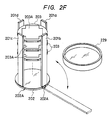
- both the pillar 201 and pillar connecting substrate 202 may be constructed as shown in Fig. 2F.
- pillar 201b among four pillars 201 is so arranged to be bent.
- a hinge is mounted between the bent pillar 201b and the pillar connecting substrate 202 at these connecting sections 202A in such a manner that it is mounted between the outer wall of the pillar 201 and the edge portion of the pillar connecting substrate 202. Since the hinge is mounted to the outer wall of the pillar 201b, the pillar is not bent inside, but allowable to be bent outside.
- a lid 229 is employed to cover it.
- the semiconductor substrate supporting members 205 shown in Fig. 2B or 2C and 210 are provided with the pillar 201 illustrated in Fig. 2F.
- Both the rear surfaces of the semiconductor wafer 203, for instance, are attached to each other, and the resultant semiconductor wafers 203 may be supported by either the semiconductor substrate supporting members 205 and 210 (see Fig. 2B), or 205 (Fig. 2C).
- the interval between the semiconductor supporting members 205, 210, and 205, into which the semiconductor wafer 203 can be inserted is made wider than that of the single semiconductor wafer 203.
- the semiconductor wafer 203 is not limited to the above-mentioned wafer, but may be such a semiconductor substrate that, for example, the peripherals of the semiconductor wafer 203 are cut off to form a rectangle-shaped semiconductor wafer.
- the layout for arranging the respective pillars 201, and the size and shape of the pillar connecting substrate 202 may be modified, depending upon the size and shape of the employed semiconductor substrate.
- the packaging device is constructed of a plurality of pillars standing around the peripherals of the semiconductor wafer, the semiconductor substrate supporting members and pillar connecting members and pillar connecting substrate mounted thereto, the semiconductor wafer can be supported thereon without any twist and vibration phenomenon. As a consequence, a large-sized semiconductor integrated circuit constructed of a semiconductor wafer can be packaged under the stable condition.
Landscapes
- Engineering & Computer Science (AREA)
- Power Engineering (AREA)
- Microelectronics & Electronic Packaging (AREA)
- Physics & Mathematics (AREA)
- Condensed Matter Physics & Semiconductors (AREA)
- General Physics & Mathematics (AREA)
- Computer Hardware Design (AREA)
- Packaging Frangible Articles (AREA)
- Design And Manufacture Of Integrated Circuits (AREA)
- Semiconductor Memories (AREA)
- Testing Or Measuring Of Semiconductors Or The Like (AREA)
- Internal Circuitry In Semiconductor Integrated Circuit Devices (AREA)
Description
- The present invention relates to the packaging of semiconductor integrated circuits according to claim 1, and more particularly to a packaging technique for semiconductor integrated circuits formed on a large-sized semiconductor substrate such as a semiconductor wafer.
- In general, semiconductor integrated circuits are constructed on respective parts of a substate, i.e. a semiconductor wafer chip the wafer then being subdivided by dicing it into a plurality of parts each corresponding to one or more integrated circuits. However, recently, constructions have been investigated in which the semiconductor wafer is not subdivided, but a plurality of integrated circuits are fabricated on the whole of the semiconductor wafer so as to construct a large-sized semiconductor integrated circuit. Such a semiconductor manufacturing technique is described in e.g. JP-A-61/290739, in which one large-sized semiconductor integrated circuit is constructed on the entire semiconductor wafer.
- There is, however, no known method of packaging a stack of large-sized semiconductor wafers where the connections to each wafer are independent of the connections to the other wafers.
- US-A-3 908 155 discloses a device for packaging a stack of wafers interconnected by a common interconnection bus. Similarly, the disclosure contained in the IBM Technical Disclosure Bulletin, vol. 17, no. 4, September 1974: "Packaging for large memory system", by H. F. Tepper, describes a packaging device where the interconnections to the wafers extend from common interconnection tabs.
- The present invention therefore proposes a stack of large sized semiconductor substrates, comprising a packaging device with a plurality of engaging means, each engaging means being for engaging a respective one of the substrates to maintain the substrates in spaced apart relationship, characterised in that:
the engaging means including means for providing a plurality of independent electrical connections to the substrate. - The engaging means may be a plurality of interconnected pillars each having means for engaging the substrates at the periphery of those substrates. This has the advantage that the wafer(s) are supported at a plurality of positions, so that the wafer(s) cannot vibrate or twist. The pillars may then be hingedly interconnected to the base, possibly via springs which holds them into engagement with the wafers.
- Thus, the present invention may provide a stack of large-sized semiconductor substrates, comprising a packaging device engaging the substrates to maintain them in a spaced apart relationship.
- The wafer(s) may then be electrically connected to the packaging device, e.g. by spring electrodes.
- Embodiments of the present invention will now be described in detail,by way of example, with reference to the accompanying drawings, in which:
- Fig. 1A is a perspective view of an entire packaging device for supporting a plurality of large-sized semiconductor substrates constructed of a semiconductor wafer;
- Fig. 1B is an enlarged perspective view of a supporting member employed in the packaging device shown in Fig. 1A;
- Fig. 1C is a side view of the supporting member;
- Fig. 1D is a side view of the modified supporting member;
- Fig. 2A is a perspective view of an entire packaging device;
- Figs. 2B and 2C are side views of a semiconductor substrate supporting member;
- Fig. 2D is a perspective view of a pillar connecting substrate 2, which is observed from its bottom side;
- Fig. 2E is a perspective view of a connection part between the pillar and the pillar connecting substrate;
- Fig. 2F is a perspective view of a modified packaging device;
- Fig. 3A is a plan view of a mounting substrate on which a plurality of semiconductor chips are mounted;
- In a semiconductor integrated circuit according to a first embodiment of the present invention, as illustrated in Fig. 1A, an
integrated circuit region 101A on which various integrated circuits have been constructed, is present on a surface of a large-sized semiconductor substrate 101 made of a semiconductor wafer. At a central portion of the above-describedsemiconductor substrate 101, arectangular opening 102 which has been formed by, for instance, etching treatment, is formed. Thesemiconductor substrate 101 is supported by an upper supportingmember 105A and a lower supportingmember 105B made of, e.g., an epoxy resin in such a manner that, arectangular pillar 103 made of, for instance, an alminium alloy or a plastic resin is pierced through theopening 102, and the substrate is sandwiched by both the upper and lower supportingmembers pillar 103. The central portion of thispillar 103 is made empty. A size of the opening 102 of thesubstrate 101 is defined under the condition that thepillar 103 can be substantially penetrated through theopening 102 while both the upper and lower supportingmembers pillar 103 is made of a metal such as aluminium, the surface of the metal pillar is covered with a resin so as to electrically insulate the wiring leads. A plurality ofconnector pins 104 are formed on the bottom of thepillar 103 so as to package thepillar 103 which mounts a plurality ofsemiconductor substrates 101, on a packaging substrate (not shown). - Both the upper and lower supporting
members pillar 103 is engaged with a supportingprojection 103A which projects from thepillar 103. Ahole 119 for penetrating a supportingshaft 114 therethrough is formed on the upper supportingmember 105A, lower supportingmember 105B, and supportingprojection 103A, respectively. That is to say, both the upper and lower supportingmembers projection 103A in such a manner that they can be rotated with respect to the supportingaxis 114 as its rotating center. To sandwich thesemiconductor substrate 101 by the upper and lower supportingmembers twist coil spring 112 is arranged on both sides of the upper and lower supportingmembers end 112A of thetwist coil spring 112 is fixed to either the upper supportingmember 105A or lower supportingmember 105B, and the supportingshaft 114 is penetrated through acentral hole 113 thereof. It is seen that onlytwist coil spring 112 of one edge of the respective upper and lower supportingmembers semiconductor substrate 101 is supported by the upper and lower supportingmembers twist coil spring 112. - A plurality of fixing electrodes are fixed on the upper surface of the upper supporting
member 105A, which are made of aluminium on which, for instance, copper or silver is plated. A plurality of brush electrodes having elasticity are provided on the side of thepillar 103 corresponding to thefixing electrodes 106, and one end of the respective brush electrodes is resiliently in contact with the surface of thecorresponding fixing electrodes 106. The end portion of therespective brush electrodes 107 which is resiliently in contact with the respective fixing electrodes, is slidable on thecorresponding fixing electrode 106 while the upper supportingmembers 105A is rotated. Anotherelectrode 110 made of, for example, cupper is provided on an inner surface of thepillar 103, in relation to the above-describedbrush electrode 107, and is connected to thebrush electrode 107 by alead 109 made of, for instance, aluminium on which silver is plated. Between thislead 109 and thepillar 103, an epoxy resin is provided for electrical insulation. Acore 108B of an electrically insulatedcable 108, the surface of which is covered with aninsulating film 108A such as a resin, vinyl chloride, is connected to thecorresponding electrode 110 by, for example,solder 111. Theinsulated cable 108 is attached to thepillar 103 by adhesive agent so that these insulated cables are employed to connect between therespective semiconductor substrates 101 provided on thepillar 103 and also thesemiconductor substrate 101 and theconnector pin 104 shown in Fig. 1A. - A
spring electrode 115 having elasticity is provided on the upper surface corresponding to therespective fixing electrodes 106 of the upper supportingmember 105A. Apin 116 made of, for example, silver-plated aluminium is mechanically and electrically connected between the spring electrode and thefixing electrode 106. Therespective spring electrodes 115 are resiliently in contact with anelectrode 120 made of, for example, an aluminium film which is provided on the surface of thesemiconductor substrate 101. Also, aspring electrode 115 is provided on the lower supportingmember 105B in order that it is used as a supporting member for sandwiching thesemiconductor substrate 101. That is to say, thesemiconductor substrate 101 is supported in such a manner that a plurality ofspring electrodes 115 respectively provided on the upper and lower supportingmembers substrate 101. - When the
semiconductor substrate 101 is loaded on thepillar 103, as illustrated in Fig. 1C, the upper and lower supportingmembers semiconductor substrate 101, which is supported by both the upper and lower supportingmembers rubber 117 made of, for instance, a sillicone rubber for preventing the horizontal vibrations is employed between the upper supportingmember 105A of thepillar 103 and the lower supportingmember 105B. - It should be noted that the
pillar 103 may be shaped as a cylinder according to the invention. In this case, it is apparent that the shape of theopening 102 formed on thesemiconductor substrate 101 may be circle. - It should also be noted that both rear surfaces of two sheets of the
semiconductor substrates 101, on which nointegrated circuit 101A is arranged, are connected to each other by the adhesive agent, and thus the connected semiconductor substrates are sandwiched by these upper and lower supportingmembers members - The following effects according to the first embodiment will be achieved.
- (1). The packaging device according to the first embodiment is so constructed that the center portion of the above-described
semiconductor substrate 101 is supported by thepillar 103 which passes through the center portion of the large-sized semiconductor substrate 101, and also by the upper and lower supportingmembers pillar 103. Accordingly, since the large-sized semiconductor substrate 101 can be supported in a stable condition, the packaging device for stably packaging thesemiconductor substrate 101 can be obtained. - (2). Since the
spring electrodes 115 are provided on the upper and lower supportingmembers semiconductor substrate 101, thesemiconductor substrate 101 can be supported and simultaneously, the electrical connection can be established between therespective semiconductor substrates 101, and also between thesemiconductor substrate 101 and the packaging substrate. - (3). As the
connector pin 104 is mounted on the bottom of thepillar 103, thepillar 103 is packaged onto the packaging substrate and simultaneously, the electrical connection can be achieved. - (4). Since the center portion of the
semiconductor substrate 101 is connected to thepillar 103, the maximum distance between this connection point and the arbitrary point on thecircuit region 101A is substantially equal to a half of the diameter of thesemiconductor wafer 101 so that a difference between the transferring speeds can be reduced. - (5). As the center portion of the
semiconductor substrate 101 is supported, and no shielding part is present around the semiconductor substrate, the heat radiation effect can be improved. - (6). Since a plurality of
semiconductor substrates 101 are mounted on thepillar 103 in such a way that these substrates are successively overlapped along thepillar 103, a large quantity of circuits can be arranged within a smaller packaging area. - The packaging device according to the invention may be constructed as packaging device as shown in Fig. 1D.
- In Fig. 1D, the
semiconductor substrate 101 has noopening 102 as illustrated in Figs. 1A to 1C. The shape of thepillar 103 is formed as a rectanglar pillar or a cylindircal pillar, the upper and lower edges of which are flat surfaces. That is to say, an interior of thepillar 103 is formed as a cavity, and both the upper and lower ends thereof are made closed. Theadhesive agent 118 is coated on both the upper and lower ends thereof are made closed. Theadhesive agent 118 is coated on both the upper and lower ends which are in turn attached to the central portion of thesemiconductor substrate 101. No integrated circuit is constructed on the portion to which thepillar 103 of thesemiconductor substrate 101 is attached. Connecting electrodes (not shown) are employed on both surfaces of thesemiconductor substrate 101, corresponding to theelectrode 115 mounted on thepillar 103. Electrical connection is made between the electrodes formed on both surfaces of thesemiconductor substrate 101 via the connecting hole which penetrates through thesemiconductor substrate 101. - The
pillar 103 andsemiconductor substrate 101 are alternately stacked from the bottom. - The advantage achieved by the above-described first embodiment will now be summarized. That is to say, since the central portion of the semiconductor substrate is supported so as to construct the packaging device, and thus, the large-sized semiconductor substrate can be stably supported, the packaging device for packaging the large-sized semiconductor substrate in a stable condition can be realized.
- In Fig. 2A,
reference numeral 203 denotes a semiconductor wafer made of a monocrystal silicon andreference numeral 203A indicates an integrated circuit region for constructing various integrated circuits. - A packaging device of a semiconductor integrated circuit according to this second embodiment includes
pillars integrated wafer 203, and apillar connecting substrate 202 which is connected to the lower end portions of thesepillars pillar 201 andpillar connecting substrate 202 are made of a resin such as an epoxy resin, or aluminium. Thesemiconductor wafer 203 is sandwiched by semiconductorsubstrate supporting members pillar 201. Among the above-describedpillars 201a to 201d, the pillars, for instance, 201b and 201c are arranged to be bent, or brought down as shown in Fig. 2E. The remainingpillars pillar connecting substrate 202. It should be noted that only thepillar 201a, threepillars 201a to 201c, or all of thepillars 201a to 201d may be bent or brought down. Thepillars 201 other than thebendable pillars 201 are fixed on thepillar connecting substrate 202. - Then, a description will now be made of the portion for supporting the
semiconductor wafer 203 of thepillar 201. - In Fig. 2B, the
semiconductor wafer 203 is supported by the upper semiconductorsubstrate supporting member 205 and the lower semiconductorsubstrate supporting member 206 mounted on thepillar 201 in the fixed condition. The upper semiconductorsubstrate supporting member 210 is made of, for instance, a resin such as an epoxy resin, or alminium, and is integrally formed with, for example, thepillar 201. The lower semiconductorsubstrate supporting member 210 is mounted on a supportingsection 201A projecting from thepillar 201 in such a manner that it is rotatable around the supportingshaft 212. The lower semiconductorsubstrate supporting member 210 is made of, for instance, a resin such as a glass epoxy resin, or aluminium. A plurality of hair-pin-shapedspring electrodes 206 are provided on the lower surface of the upper semiconductorsubstrate supporting member 205 so as to be resiliently connected to theelectrode 204 of thesemiconductor wafer 203. Thespring electrode 206 is connected via anembeded wiring lead 207 which penetrates through the upper semiconductorsubstrate supporting member 205, and theupper wiring lead 208 of the upper surface of the upper semiconductorsubstrate supporting member 205, to aterminal electrode 214 provided on the outer wall of thepillar 201. Thewiring lead 208 penetrates through a through hole formed on thepillar 201. To achieve the better contact between the lower semiconductorsubstrate supporting member 201 and thesemiconductor wafer 203, the hair-pin-shapedpressure spring 211 is provided on the upper surface of the lower semiconductorsubstrate supporting member 210, i.e., the plane opposite to thesemiconductor wafer 203. By connecting by thecoil spring 209 between the upper semiconductorsubstrate supporting member 205 and the lower semiconductorsubstrate supporting member 210, both the force required for sandwiching thesemiconductor wafer 203 by means of both the upper and lower semiconductorsubstrate supporting members spring electrode 206 to theelectrode 204 of thesemiconductor wafer 203. The portion on which thecoil spring 209 of the lower semiconductorsubstrate supporting member 210 is located at the side of thesemiconductor wafer 203 rather than the supportingaxis 212. Ahandle 213 is mounted on the lower surface of the lower semiconductorsubstrate supporting member 210 so as to open a space defined between the upper and lower semiconductorsubstrate supporting members semiconductor wafer 203. The above-described upper semiconductorsubstrate supporting member 205, lower semiconductorsubstrate supporting member 210, andcoil spring 209 are mounted on the correspondingpillars semiconductor wafer 203 can be sandwiched at four positions under the stable condition. Furthermore, the above-describedspring electrode 206, wiring leads 207 and 208,coil spring 209 andpressure spring 211 are mounted on the respective upper and lowersubstrate supporting members pillars 201. With respect to thespring electrode 206, theelectrode 204 is arranged to thesemiconductor wafer 203. - To the
terminal electrode 214 at the outer wall of thepillar 201, acore 215A of acable 215 which is insulating-covered with vinyle chloride is connected by solder. This insulatingcable 215 connects therespective semiconductor wafers 203, and thesemiconductor wafers 203 packaged on the packaging substrate and also the wiring lines on the packaging substrate. - A sandwiching member of the
semiconductor wafer 203, as illustrated in Fig. 2C, is provided in such a manner that the semiconductor wafer supporting, or sandwichingmember 205 is ⊐-shaped, and both thespring electrode 206 andpressure spring 211 are fixed on the side surface of the inside thereof. Thepillar 201 defines acavity 218 of a cylindrical form at the portion corresponding to the semiconductorsubstrate supporting member 205 in order to fit with the semiconductorsubstrate supporting member 205. The semiconductorsubstrate supporting member 205 fitted within thiscavity 218 is positioned to be depressed by thecoil spring 219. Aterminal electrode 217 is provided on the upper surface of the semiconductorsubstrate supporting member 205, to which thecore 215A of thecable 215 is connected. Thecable 215 extends over the plane opposite to thesemiconductor wafer 203, i.e., the outer wall of thepillar 201. Thiscable 215 is connected via a through hole formed on thepillar 201 adjacent to the semiconductorsubstrate supporting member 215 to theterminal electrode 216. To achieve the better connection between thespring electrode 206 and theelectrode 204 and also firmly sandwich thesemiconductor wafer 203, an interval between thespring electrode 206 andpressure spring 211 by which thesemiconductor wafer 203 is not yet mounted, is narrower than the thickness of thesemiconductor wafer 203. - As illustrated in Fig. 2D, a plurality of connector pins 221 connected to the
cable 215, as illustrated in Fig. 2B or 2C, are provided on the bottom of thepillar connecting substrate 202. These connector pins 221 are connected to the connector for the packaging substrate. Since thepillar connecting substrate 202 is mounted to the packaging substrate by screws during the packaging operation, a plurality of screw holes 220 are formed. - One example of the connection between the lower end portion of the
pillar 201 and thepillar connecting substrate 202 is shown in Fig. 2E. As shown in Fig. 2E, the connecting portion of thepillar connecting substrate 202 is engaged with the lower portion of thepillar 201, and rotatably connected in such a manner that a mountingbolt 227 is inserted into thecorresponding bolt hole 230 formed on these portions. Thebolt 227 is so arranged that it is not dropped from thecorresponding bolt hole 230 by mounting anut 228 on thescrew section 227. Atwist coil spring 222 is positioned on both sides of the pillar and thebolt 227 is penetrated through the respective center holes 226. One end of thistwist coil spring 222 is mounted in thespring mounting hole 223 of thepillar connecting substrate 202, whereas the other end thereof is mounted in thespring mounting hole 225 formed on the projecting 224 of thepillar 201. Thepillar 201 can be stood up at a right angle by thistwist coil spring 222, and also thebent pillar 201 can be recovered by means of thetwist coil spring 222. - It should be noted that both the
pillar 201 andpillar connecting substrate 202 may be constructed as shown in Fig. 2F. - In Fig. 2F, one
pillar 201b among fourpillars 201 is so arranged to be bent. A hinge is mounted between thebent pillar 201b and thepillar connecting substrate 202 at these connectingsections 202A in such a manner that it is mounted between the outer wall of thepillar 201 and the edge portion of thepillar connecting substrate 202. Since the hinge is mounted to the outer wall of thepillar 201b, the pillar is not bent inside, but allowable to be bent outside. In order to prevent the standingpillar 201b from being bent inside, alid 229 is employed to cover it. Also the semiconductorsubstrate supporting members 205 shown in Fig. 2B or 2C and 210 are provided with thepillar 201 illustrated in Fig. 2F. - The following various merits can be achieved according to the above-described packaging device of this second embodiment.
- (1). The packaging device is constructed of a plurality of
pillars 201 which stand at the peripheral portion of the semiconductor wafer 1, the semiconductorsubstrate supporting members pillar connecting substrate 202. As a result, thesemiconductor wafer 203 can be supported without twist and vibrations, so that a large-sized semiconductor integrated circuit constructed of thesemiconductor wafer 203 can be packaged in the stable condition. - (2) Since the
connector pin 221 is mounted on the bottom of thepillar connecting substrate 202, the integrated circuits can be connected to the packaging substrate in such a manner that the stable supporting condition for thesemiconductor wafer 203 is not disturbed, in other words, thesemiconductor wafer 203 is not bent. - (3). The
spring electrode 206 is provided on the semiconductorsubstrate supporting member 205, with the result that both thesemiconductor wafer 203 can be sandwiched and simultaneously the electrical connection can be realized. - (4). As the electrode mounted on the semiconductor
substrate supporting member 205 is used as thespring electrode 206, the sandwich effect by thesemiconductor wafer 203 can be improved so as to electrically connect the corresponding portions. - (5). Since the
twist coil spring 222 orlid 229 for standing thepillar 203 is employed, thepillar 201 may not be bent while supporting thesemiconductor wafer 203, so that the stable supporting condition of thesemiconductor wafer 203 can be maintained for a long time. - (6). A plurality of
semiconductor wafers 203 can be mounted on thepillar 201, with the result that a large circuit system can be arranged with a smaller packaging area. - (7). Since the
pillar 203 can be bent, thesubstrate wafer 203 can be mounted in the horizontal direction while bending thepillar 203. As a result, thesemiconductor wafer 203 can be easily mounted. - While the present invention has been described using a specific embodiment, it should be noted that further modifications and changes can be made without departing from the scope of the present invention.
- Both the rear surfaces of the
semiconductor wafer 203, for instance, are attached to each other, and theresultant semiconductor wafers 203 may be supported by either the semiconductorsubstrate supporting members 205 and 210 (see Fig. 2B), or 205 (Fig. 2C). In this case, the interval between thesemiconductor supporting members semiconductor wafer 203 can be inserted, is made wider than that of thesingle semiconductor wafer 203. - Also, the
semiconductor wafer 203 is not limited to the above-mentioned wafer, but may be such a semiconductor substrate that, for example, the peripherals of thesemiconductor wafer 203 are cut off to form a rectangle-shaped semiconductor wafer. In this case, the layout for arranging therespective pillars 201, and the size and shape of thepillar connecting substrate 202 may be modified, depending upon the size and shape of the employed semiconductor substrate. - The advantage achieved by the above-mentioned second embodiment will now be briefly described.
- That is to say, since the packaging device is constructed of a plurality of pillars standing around the peripherals of the semiconductor wafer, the semiconductor substrate supporting members and pillar connecting members and pillar connecting substrate mounted thereto, the semiconductor wafer can be supported thereon without any twist and vibration phenomenon. As a consequence, a large-sized semiconductor integrated circuit constructed of a semiconductor wafer can be packaged under the stable condition.
Claims (8)
- A stack of large sized semiconductor substrates, comprising a packaging device with a plurality of engaging means, each engaging means being for engaging a respective one of the substrates to maintain the substrates in spaced apart relationship, characterised in that:
the engaging means including means for providing a plurality of independent electrical connections to the substrate. - A stack according to claim 1, wherein the packaging device engages the substrates at a central part of those substrates.
- A stack according to claim 2, wherein each substrate has an opening at a central part thereof, and the packaging device comprises an elongate pillar extending through those openings and engaging each substrate at or adjacent the opening.
- A stack according to claim 1, wherein the packaging device comprises a plurality of interconnected pillars each having means for engaging the substrates at the periphery of those substrates.
- A stack according to claim 4, wherein the pillars are interconnected by a base, and the pillars are hinged to that base.
- A stack according to claim 5, wherein the pillars are hinged to the base via a spring, biasing the pillars into engagement with the substrates.
- A stack according to any one of the preceding claims, wherein the packaging device has means for making electrical contact with each substrate.
- A stack according to claim 7, wherein the means for making connection is a spring electrode.
Priority Applications (1)
| Application Number | Priority Date | Filing Date | Title |
|---|---|---|---|
| EP92112517A EP0516185B1 (en) | 1987-04-22 | 1988-04-08 | Wafer-scale semiconductor integrated circuit device |
Applications Claiming Priority (10)
| Application Number | Priority Date | Filing Date | Title |
|---|---|---|---|
| JP62097330A JPS63263734A (en) | 1987-04-22 | 1987-04-22 | Mounting device for semiconductor integrated circuit |
| JP97330/87 | 1987-04-22 | ||
| JP62097331A JPS63263735A (en) | 1987-04-22 | 1987-04-22 | Mounting device for semiconductor integrated circuit |
| JP97329/87 | 1987-04-22 | ||
| JP97331/87 | 1987-04-22 | ||
| JP62097326A JPS63263747A (en) | 1987-04-22 | 1987-04-22 | Manufacture of mounting board |
| JP62097329A JPS63263736A (en) | 1987-04-22 | 1987-04-22 | Semiconductor device |
| JP97326/87 | 1987-04-22 | ||
| JP99779/87 | 1987-04-24 | ||
| JP62099779A JPS63266700A (en) | 1987-04-24 | 1987-04-24 | Wafer-sized semiconductor integrated circuit device |
Related Child Applications (1)
| Application Number | Title | Priority Date | Filing Date |
|---|---|---|---|
| EP92112517.5 Division-Into | 1992-07-22 |
Publications (3)
| Publication Number | Publication Date |
|---|---|
| EP0288186A2 EP0288186A2 (en) | 1988-10-26 |
| EP0288186A3 EP0288186A3 (en) | 1990-05-23 |
| EP0288186B1 true EP0288186B1 (en) | 1993-06-30 |
Family
ID=27525857
Family Applications (2)
| Application Number | Title | Priority Date | Filing Date |
|---|---|---|---|
| EP92112517A Expired - Lifetime EP0516185B1 (en) | 1987-04-22 | 1988-04-08 | Wafer-scale semiconductor integrated circuit device |
| EP88303160A Expired - Lifetime EP0288186B1 (en) | 1987-04-22 | 1988-04-08 | Packaging of semiconductor integrated circuits |
Family Applications Before (1)
| Application Number | Title | Priority Date | Filing Date |
|---|---|---|---|
| EP92112517A Expired - Lifetime EP0516185B1 (en) | 1987-04-22 | 1988-04-08 | Wafer-scale semiconductor integrated circuit device |
Country Status (5)
| Country | Link |
|---|---|
| EP (2) | EP0516185B1 (en) |
| KR (2) | KR960012649B1 (en) |
| DE (2) | DE3856019T2 (en) |
| HK (2) | HK28096A (en) |
| SG (1) | SG36588G (en) |
Families Citing this family (5)
| Publication number | Priority date | Publication date | Assignee | Title |
|---|---|---|---|---|
| WO1995000973A1 (en) * | 1993-06-23 | 1995-01-05 | Vlsi Technology, Inc. | Electrically and thermally enhanced package using a separate silicon substrate |
| US5598031A (en) * | 1993-06-23 | 1997-01-28 | Vlsi Technology, Inc. | Electrically and thermally enhanced package using a separate silicon substrate |
| EP0849738A3 (en) * | 1996-12-19 | 1999-04-21 | Texas Instruments Incorporated | Improvements in or relating to electronic systems |
| JP2001102523A (en) * | 1999-09-28 | 2001-04-13 | Sony Corp | Thin-film device and manufacturing method therefor |
| JP2003229517A (en) * | 2002-01-31 | 2003-08-15 | Fujitsu Hitachi Plasma Display Ltd | Semiconductor chip mounted substrate and flat display |
Family Cites Families (4)
| Publication number | Priority date | Publication date | Assignee | Title |
|---|---|---|---|---|
| US3908155A (en) * | 1974-04-19 | 1975-09-23 | Ibm | Wafer circuit package |
| DE2611749C3 (en) * | 1976-03-19 | 1980-11-13 | Siemens Ag, 1000 Berlin Und 8000 Muenchen | Semiconductor arrangement with a semiconductor component that can be contacted by pressure via clamping bolts |
| JPS5618439A (en) * | 1979-07-25 | 1981-02-21 | Fujitsu Ltd | Semiconductor device consisting of different ic |
| JPH0620107B2 (en) * | 1985-09-25 | 1994-03-16 | 日本電気株式会社 | Semiconductor device |
-
1988
- 1988-03-29 KR KR88003425A patent/KR960012649B1/en not_active IP Right Cessation
- 1988-04-08 EP EP92112517A patent/EP0516185B1/en not_active Expired - Lifetime
- 1988-04-08 EP EP88303160A patent/EP0288186B1/en not_active Expired - Lifetime
- 1988-04-08 DE DE3856019T patent/DE3856019T2/en not_active Expired - Fee Related
- 1988-04-08 DE DE88303160T patent/DE3882074T2/en not_active Expired - Fee Related
- 1988-04-08 SG SG1995905451A patent/SG36588G/en unknown
-
1993
- 1993-03-18 KR KR93004115A patent/KR970001885B1/en not_active IP Right Cessation
-
1996
- 1996-02-15 HK HK28096A patent/HK28096A/en unknown
-
1998
- 1998-03-02 HK HK98101603A patent/HK1003348A1/en not_active IP Right Cessation
Also Published As
| Publication number | Publication date |
|---|---|
| HK1003348A1 (en) | 1998-10-23 |
| EP0516185A3 (en) | 1993-03-17 |
| EP0288186A2 (en) | 1988-10-26 |
| SG36588G (en) | 1995-09-01 |
| KR970001885B1 (en) | 1997-02-18 |
| DE3856019D1 (en) | 1997-10-09 |
| KR880013223A (en) | 1988-11-30 |
| DE3882074T2 (en) | 1993-10-07 |
| KR930020560A (en) | 1993-10-20 |
| EP0516185A2 (en) | 1992-12-02 |
| EP0288186A3 (en) | 1990-05-23 |
| EP0516185B1 (en) | 1997-09-03 |
| DE3882074D1 (en) | 1993-08-05 |
| HK28096A (en) | 1996-02-23 |
| DE3856019T2 (en) | 1998-04-02 |
| KR960012649B1 (en) | 1996-09-23 |
Similar Documents
| Publication | Publication Date | Title |
|---|---|---|
| US6078501A (en) | Power semiconductor module | |
| US4225900A (en) | Integrated circuit device package interconnect means | |
| KR100277308B1 (en) | Semiconductor device | |
| US6344683B1 (en) | Stacked semiconductor package with flexible tape | |
| US6343019B1 (en) | Apparatus and method of stacking die on a substrate | |
| US6175159B1 (en) | Semiconductor package | |
| US4941033A (en) | Semiconductor integrated circuit device | |
| US5933710A (en) | Method of providing electrical connection between an integrated circuit die and a printed circuit board | |
| US5172303A (en) | Electronic component assembly | |
| EP0352429B1 (en) | High power, pluggable tape automated bonding package | |
| US5777382A (en) | Plastic packaging for a surface mounted integrated circuit | |
| JPS6355213B2 (en) | ||
| KR20010034154A (en) | Semiconductor component with several substrate layers and at least one semiconductor chip and method for producing a semiconductor component | |
| JP2932432B2 (en) | Semiconductor package structure and packaging method | |
| JPH08306723A (en) | Electronic circuit board and its preparation | |
| EP1429389A1 (en) | Compact circuit module having high mounting accuracy and method of manufacturing the same | |
| US6987313B2 (en) | Semiconductor device | |
| EP0288186B1 (en) | Packaging of semiconductor integrated circuits | |
| US5455741A (en) | Wire-lead through hole interconnect device | |
| JPH04297043A (en) | Interconnection method for vertical semiconductor and constituent body | |
| EP0924845A2 (en) | Power semiconductor module | |
| US5734196A (en) | Electronic packaging shaped beam lead fabrication | |
| EP0282124B1 (en) | Method for manufacturing a modular semiconductor power device and device obtained thereby | |
| US20020027272A1 (en) | Semiconductor device, semiconductor package for use therein, and manufacturing method thereof | |
| KR20030075385A (en) | Chip scale package and method of fabricating the same |
Legal Events
| Date | Code | Title | Description |
|---|---|---|---|
| PUAI | Public reference made under article 153(3) epc to a published international application that has entered the european phase |
Free format text: ORIGINAL CODE: 0009012 |
|
| AK | Designated contracting states |
Kind code of ref document: A2 Designated state(s): DE FR GB IT |
|
| PUAL | Search report despatched |
Free format text: ORIGINAL CODE: 0009013 |
|
| AK | Designated contracting states |
Kind code of ref document: A3 Designated state(s): DE FR GB IT |
|
| 17P | Request for examination filed |
Effective date: 19900927 |
|
| 17Q | First examination report despatched |
Effective date: 19910919 |
|
| GRAA | (expected) grant |
Free format text: ORIGINAL CODE: 0009210 |
|
| AK | Designated contracting states |
Kind code of ref document: B1 Designated state(s): DE FR GB IT |
|
| XX | Miscellaneous (additional remarks) |
Free format text: TEILANMELDUNG 92112517.5 EINGEREICHT AM 08/04/88. |
|
| REF | Corresponds to: |
Ref document number: 3882074 Country of ref document: DE Date of ref document: 19930805 |
|
| ET | Fr: translation filed | ||
| ITF | It: translation for a ep patent filed |
Owner name: MODIANO & ASSOCIATI S.R |
|
| PLBE | No opposition filed within time limit |
Free format text: ORIGINAL CODE: 0009261 |
|
| STAA | Information on the status of an ep patent application or granted ep patent |
Free format text: STATUS: NO OPPOSITION FILED WITHIN TIME LIMIT |
|
| 26N | No opposition filed | ||
| PGFP | Annual fee paid to national office [announced via postgrant information from national office to epo] |
Ref country code: GB Payment date: 19950329 Year of fee payment: 8 |
|
| PGFP | Annual fee paid to national office [announced via postgrant information from national office to epo] |
Ref country code: FR Payment date: 19950418 Year of fee payment: 8 |
|
| PGFP | Annual fee paid to national office [announced via postgrant information from national office to epo] |
Ref country code: DE Payment date: 19950626 Year of fee payment: 8 |
|
| PG25 | Lapsed in a contracting state [announced via postgrant information from national office to epo] |
Ref country code: GB Effective date: 19960408 |
|
| GBPC | Gb: european patent ceased through non-payment of renewal fee |
Effective date: 19960408 |
|
| PG25 | Lapsed in a contracting state [announced via postgrant information from national office to epo] |
Ref country code: FR Effective date: 19961227 |
|
| PG25 | Lapsed in a contracting state [announced via postgrant information from national office to epo] |
Ref country code: DE Effective date: 19970101 |
|
| REG | Reference to a national code |
Ref country code: FR Ref legal event code: ST |
|
| PG25 | Lapsed in a contracting state [announced via postgrant information from national office to epo] |
Ref country code: IT Free format text: LAPSE BECAUSE OF NON-PAYMENT OF DUE FEES;WARNING: LAPSES OF ITALIAN PATENTS WITH EFFECTIVE DATE BEFORE 2007 MAY HAVE OCCURRED AT ANY TIME BEFORE 2007. THE CORRECT EFFECTIVE DATE MAY BE DIFFERENT FROM THE ONE RECORDED. Effective date: 20050408 |