EP0288186A2 - Packaging of semiconductor integrated circuits - Google Patents
Packaging of semiconductor integrated circuits Download PDFInfo
- Publication number
- EP0288186A2 EP0288186A2 EP88303160A EP88303160A EP0288186A2 EP 0288186 A2 EP0288186 A2 EP 0288186A2 EP 88303160 A EP88303160 A EP 88303160A EP 88303160 A EP88303160 A EP 88303160A EP 0288186 A2 EP0288186 A2 EP 0288186A2
- Authority
- EP
- European Patent Office
- Prior art keywords
- semiconductor
- substrate
- pillar
- pillars
- wafer
- Prior art date
- Legal status (The legal status is an assumption and is not a legal conclusion. Google has not performed a legal analysis and makes no representation as to the accuracy of the status listed.)
- Granted
Links
Images


Classifications
-
- H—ELECTRICITY
- H01—ELECTRIC ELEMENTS
- H01L—SEMICONDUCTOR DEVICES NOT COVERED BY CLASS H10
- H01L23/00—Details of semiconductor or other solid state devices
- H01L23/12—Mountings, e.g. non-detachable insulating substrates
-
- H—ELECTRICITY
- H01—ELECTRIC ELEMENTS
- H01L—SEMICONDUCTOR DEVICES NOT COVERED BY CLASS H10
- H01L23/00—Details of semiconductor or other solid state devices
- H01L23/52—Arrangements for conducting electric current within the device in operation from one component to another, i.e. interconnections, e.g. wires, lead frames
- H01L23/538—Arrangements for conducting electric current within the device in operation from one component to another, i.e. interconnections, e.g. wires, lead frames the interconnection structure between a plurality of semiconductor chips being formed on, or in, insulating substrates
- H01L23/5385—Assembly of a plurality of insulating substrates
-
- H—ELECTRICITY
- H01—ELECTRIC ELEMENTS
- H01L—SEMICONDUCTOR DEVICES NOT COVERED BY CLASS H10
- H01L23/00—Details of semiconductor or other solid state devices
- H01L23/12—Mountings, e.g. non-detachable insulating substrates
- H01L23/14—Mountings, e.g. non-detachable insulating substrates characterised by the material or its electrical properties
- H01L23/147—Semiconductor insulating substrates
-
- H—ELECTRICITY
- H01—ELECTRIC ELEMENTS
- H01L—SEMICONDUCTOR DEVICES NOT COVERED BY CLASS H10
- H01L23/00—Details of semiconductor or other solid state devices
- H01L23/32—Holders for supporting the complete device in operation, i.e. detachable fixtures
-
- H—ELECTRICITY
- H01—ELECTRIC ELEMENTS
- H01L—SEMICONDUCTOR DEVICES NOT COVERED BY CLASS H10
- H01L25/00—Assemblies consisting of a plurality of individual semiconductor or other solid state devices ; Multistep manufacturing processes thereof
- H01L25/03—Assemblies consisting of a plurality of individual semiconductor or other solid state devices ; Multistep manufacturing processes thereof all the devices being of a type provided for in the same subgroup of groups H01L27/00 - H01L33/00, or in a single subclass of H10K, H10N, e.g. assemblies of rectifier diodes
- H01L25/04—Assemblies consisting of a plurality of individual semiconductor or other solid state devices ; Multistep manufacturing processes thereof all the devices being of a type provided for in the same subgroup of groups H01L27/00 - H01L33/00, or in a single subclass of H10K, H10N, e.g. assemblies of rectifier diodes the devices not having separate containers
- H01L25/065—Assemblies consisting of a plurality of individual semiconductor or other solid state devices ; Multistep manufacturing processes thereof all the devices being of a type provided for in the same subgroup of groups H01L27/00 - H01L33/00, or in a single subclass of H10K, H10N, e.g. assemblies of rectifier diodes the devices not having separate containers the devices being of a type provided for in group H01L27/00
- H01L25/0652—Assemblies consisting of a plurality of individual semiconductor or other solid state devices ; Multistep manufacturing processes thereof all the devices being of a type provided for in the same subgroup of groups H01L27/00 - H01L33/00, or in a single subclass of H10K, H10N, e.g. assemblies of rectifier diodes the devices not having separate containers the devices being of a type provided for in group H01L27/00 the devices being arranged next and on each other, i.e. mixed assemblies
-
- H—ELECTRICITY
- H01—ELECTRIC ELEMENTS
- H01L—SEMICONDUCTOR DEVICES NOT COVERED BY CLASS H10
- H01L25/00—Assemblies consisting of a plurality of individual semiconductor or other solid state devices ; Multistep manufacturing processes thereof
- H01L25/03—Assemblies consisting of a plurality of individual semiconductor or other solid state devices ; Multistep manufacturing processes thereof all the devices being of a type provided for in the same subgroup of groups H01L27/00 - H01L33/00, or in a single subclass of H10K, H10N, e.g. assemblies of rectifier diodes
- H01L25/04—Assemblies consisting of a plurality of individual semiconductor or other solid state devices ; Multistep manufacturing processes thereof all the devices being of a type provided for in the same subgroup of groups H01L27/00 - H01L33/00, or in a single subclass of H10K, H10N, e.g. assemblies of rectifier diodes the devices not having separate containers
- H01L25/07—Assemblies consisting of a plurality of individual semiconductor or other solid state devices ; Multistep manufacturing processes thereof all the devices being of a type provided for in the same subgroup of groups H01L27/00 - H01L33/00, or in a single subclass of H10K, H10N, e.g. assemblies of rectifier diodes the devices not having separate containers the devices being of a type provided for in group H01L29/00
- H01L25/073—Apertured devices mounted on one or more rods passed through the apertures
-
- H—ELECTRICITY
- H01—ELECTRIC ELEMENTS
- H01L—SEMICONDUCTOR DEVICES NOT COVERED BY CLASS H10
- H01L2224/00—Indexing scheme for arrangements for connecting or disconnecting semiconductor or solid-state bodies and methods related thereto as covered by H01L24/00
- H01L2224/01—Means for bonding being attached to, or being formed on, the surface to be connected, e.g. chip-to-package, die-attach, "first-level" interconnects; Manufacturing methods related thereto
- H01L2224/02—Bonding areas; Manufacturing methods related thereto
- H01L2224/04—Structure, shape, material or disposition of the bonding areas prior to the connecting process
- H01L2224/0401—Bonding areas specifically adapted for bump connectors, e.g. under bump metallisation [UBM]
-
- H—ELECTRICITY
- H01—ELECTRIC ELEMENTS
- H01L—SEMICONDUCTOR DEVICES NOT COVERED BY CLASS H10
- H01L2224/00—Indexing scheme for arrangements for connecting or disconnecting semiconductor or solid-state bodies and methods related thereto as covered by H01L24/00
- H01L2224/01—Means for bonding being attached to, or being formed on, the surface to be connected, e.g. chip-to-package, die-attach, "first-level" interconnects; Manufacturing methods related thereto
- H01L2224/02—Bonding areas; Manufacturing methods related thereto
- H01L2224/04—Structure, shape, material or disposition of the bonding areas prior to the connecting process
- H01L2224/05—Structure, shape, material or disposition of the bonding areas prior to the connecting process of an individual bonding area
- H01L2224/0554—External layer
- H01L2224/05599—Material
-
- H—ELECTRICITY
- H01—ELECTRIC ELEMENTS
- H01L—SEMICONDUCTOR DEVICES NOT COVERED BY CLASS H10
- H01L2224/00—Indexing scheme for arrangements for connecting or disconnecting semiconductor or solid-state bodies and methods related thereto as covered by H01L24/00
- H01L2224/01—Means for bonding being attached to, or being formed on, the surface to be connected, e.g. chip-to-package, die-attach, "first-level" interconnects; Manufacturing methods related thereto
- H01L2224/10—Bump connectors; Manufacturing methods related thereto
- H01L2224/15—Structure, shape, material or disposition of the bump connectors after the connecting process
- H01L2224/16—Structure, shape, material or disposition of the bump connectors after the connecting process of an individual bump connector
- H01L2224/161—Disposition
- H01L2224/16151—Disposition the bump connector connecting between a semiconductor or solid-state body and an item not being a semiconductor or solid-state body, e.g. chip-to-substrate, chip-to-passive
- H01L2224/16221—Disposition the bump connector connecting between a semiconductor or solid-state body and an item not being a semiconductor or solid-state body, e.g. chip-to-substrate, chip-to-passive the body and the item being stacked
- H01L2224/16225—Disposition the bump connector connecting between a semiconductor or solid-state body and an item not being a semiconductor or solid-state body, e.g. chip-to-substrate, chip-to-passive the body and the item being stacked the item being non-metallic, e.g. insulating substrate with or without metallisation
-
- H—ELECTRICITY
- H01—ELECTRIC ELEMENTS
- H01L—SEMICONDUCTOR DEVICES NOT COVERED BY CLASS H10
- H01L2224/00—Indexing scheme for arrangements for connecting or disconnecting semiconductor or solid-state bodies and methods related thereto as covered by H01L24/00
- H01L2224/01—Means for bonding being attached to, or being formed on, the surface to be connected, e.g. chip-to-package, die-attach, "first-level" interconnects; Manufacturing methods related thereto
- H01L2224/26—Layer connectors, e.g. plate connectors, solder or adhesive layers; Manufacturing methods related thereto
- H01L2224/31—Structure, shape, material or disposition of the layer connectors after the connecting process
- H01L2224/32—Structure, shape, material or disposition of the layer connectors after the connecting process of an individual layer connector
- H01L2224/321—Disposition
- H01L2224/32151—Disposition the layer connector connecting between a semiconductor or solid-state body and an item not being a semiconductor or solid-state body, e.g. chip-to-substrate, chip-to-passive
- H01L2224/32221—Disposition the layer connector connecting between a semiconductor or solid-state body and an item not being a semiconductor or solid-state body, e.g. chip-to-substrate, chip-to-passive the body and the item being stacked
- H01L2224/32225—Disposition the layer connector connecting between a semiconductor or solid-state body and an item not being a semiconductor or solid-state body, e.g. chip-to-substrate, chip-to-passive the body and the item being stacked the item being non-metallic, e.g. insulating substrate with or without metallisation
-
- H—ELECTRICITY
- H01—ELECTRIC ELEMENTS
- H01L—SEMICONDUCTOR DEVICES NOT COVERED BY CLASS H10
- H01L2224/00—Indexing scheme for arrangements for connecting or disconnecting semiconductor or solid-state bodies and methods related thereto as covered by H01L24/00
- H01L2224/01—Means for bonding being attached to, or being formed on, the surface to be connected, e.g. chip-to-package, die-attach, "first-level" interconnects; Manufacturing methods related thereto
- H01L2224/42—Wire connectors; Manufacturing methods related thereto
- H01L2224/44—Structure, shape, material or disposition of the wire connectors prior to the connecting process
- H01L2224/45—Structure, shape, material or disposition of the wire connectors prior to the connecting process of an individual wire connector
- H01L2224/45001—Core members of the connector
- H01L2224/45099—Material
- H01L2224/451—Material with a principal constituent of the material being a metal or a metalloid, e.g. boron (B), silicon (Si), germanium (Ge), arsenic (As), antimony (Sb), tellurium (Te) and polonium (Po), and alloys thereof
- H01L2224/45117—Material with a principal constituent of the material being a metal or a metalloid, e.g. boron (B), silicon (Si), germanium (Ge), arsenic (As), antimony (Sb), tellurium (Te) and polonium (Po), and alloys thereof the principal constituent melting at a temperature of greater than or equal to 400°C and less than 950°C
- H01L2224/45124—Aluminium (Al) as principal constituent
-
- H—ELECTRICITY
- H01—ELECTRIC ELEMENTS
- H01L—SEMICONDUCTOR DEVICES NOT COVERED BY CLASS H10
- H01L2224/00—Indexing scheme for arrangements for connecting or disconnecting semiconductor or solid-state bodies and methods related thereto as covered by H01L24/00
- H01L2224/01—Means for bonding being attached to, or being formed on, the surface to be connected, e.g. chip-to-package, die-attach, "first-level" interconnects; Manufacturing methods related thereto
- H01L2224/42—Wire connectors; Manufacturing methods related thereto
- H01L2224/44—Structure, shape, material or disposition of the wire connectors prior to the connecting process
- H01L2224/45—Structure, shape, material or disposition of the wire connectors prior to the connecting process of an individual wire connector
- H01L2224/45001—Core members of the connector
- H01L2224/45099—Material
- H01L2224/451—Material with a principal constituent of the material being a metal or a metalloid, e.g. boron (B), silicon (Si), germanium (Ge), arsenic (As), antimony (Sb), tellurium (Te) and polonium (Po), and alloys thereof
- H01L2224/45138—Material with a principal constituent of the material being a metal or a metalloid, e.g. boron (B), silicon (Si), germanium (Ge), arsenic (As), antimony (Sb), tellurium (Te) and polonium (Po), and alloys thereof the principal constituent melting at a temperature of greater than or equal to 950°C and less than 1550°C
- H01L2224/45139—Silver (Ag) as principal constituent
-
- H—ELECTRICITY
- H01—ELECTRIC ELEMENTS
- H01L—SEMICONDUCTOR DEVICES NOT COVERED BY CLASS H10
- H01L2224/00—Indexing scheme for arrangements for connecting or disconnecting semiconductor or solid-state bodies and methods related thereto as covered by H01L24/00
- H01L2224/01—Means for bonding being attached to, or being formed on, the surface to be connected, e.g. chip-to-package, die-attach, "first-level" interconnects; Manufacturing methods related thereto
- H01L2224/42—Wire connectors; Manufacturing methods related thereto
- H01L2224/44—Structure, shape, material or disposition of the wire connectors prior to the connecting process
- H01L2224/45—Structure, shape, material or disposition of the wire connectors prior to the connecting process of an individual wire connector
- H01L2224/45001—Core members of the connector
- H01L2224/45099—Material
- H01L2224/451—Material with a principal constituent of the material being a metal or a metalloid, e.g. boron (B), silicon (Si), germanium (Ge), arsenic (As), antimony (Sb), tellurium (Te) and polonium (Po), and alloys thereof
- H01L2224/45138—Material with a principal constituent of the material being a metal or a metalloid, e.g. boron (B), silicon (Si), germanium (Ge), arsenic (As), antimony (Sb), tellurium (Te) and polonium (Po), and alloys thereof the principal constituent melting at a temperature of greater than or equal to 950°C and less than 1550°C
- H01L2224/45144—Gold (Au) as principal constituent
-
- H—ELECTRICITY
- H01—ELECTRIC ELEMENTS
- H01L—SEMICONDUCTOR DEVICES NOT COVERED BY CLASS H10
- H01L2224/00—Indexing scheme for arrangements for connecting or disconnecting semiconductor or solid-state bodies and methods related thereto as covered by H01L24/00
- H01L2224/01—Means for bonding being attached to, or being formed on, the surface to be connected, e.g. chip-to-package, die-attach, "first-level" interconnects; Manufacturing methods related thereto
- H01L2224/42—Wire connectors; Manufacturing methods related thereto
- H01L2224/47—Structure, shape, material or disposition of the wire connectors after the connecting process
- H01L2224/48—Structure, shape, material or disposition of the wire connectors after the connecting process of an individual wire connector
- H01L2224/4805—Shape
- H01L2224/4809—Loop shape
- H01L2224/48091—Arched
-
- H—ELECTRICITY
- H01—ELECTRIC ELEMENTS
- H01L—SEMICONDUCTOR DEVICES NOT COVERED BY CLASS H10
- H01L2224/00—Indexing scheme for arrangements for connecting or disconnecting semiconductor or solid-state bodies and methods related thereto as covered by H01L24/00
- H01L2224/01—Means for bonding being attached to, or being formed on, the surface to be connected, e.g. chip-to-package, die-attach, "first-level" interconnects; Manufacturing methods related thereto
- H01L2224/42—Wire connectors; Manufacturing methods related thereto
- H01L2224/47—Structure, shape, material or disposition of the wire connectors after the connecting process
- H01L2224/48—Structure, shape, material or disposition of the wire connectors after the connecting process of an individual wire connector
- H01L2224/484—Connecting portions
- H01L2224/48463—Connecting portions the connecting portion on the bonding area of the semiconductor or solid-state body being a ball bond
- H01L2224/48464—Connecting portions the connecting portion on the bonding area of the semiconductor or solid-state body being a ball bond the other connecting portion not on the bonding area also being a ball bond, i.e. ball-to-ball
-
- H—ELECTRICITY
- H01—ELECTRIC ELEMENTS
- H01L—SEMICONDUCTOR DEVICES NOT COVERED BY CLASS H10
- H01L2224/00—Indexing scheme for arrangements for connecting or disconnecting semiconductor or solid-state bodies and methods related thereto as covered by H01L24/00
- H01L2224/01—Means for bonding being attached to, or being formed on, the surface to be connected, e.g. chip-to-package, die-attach, "first-level" interconnects; Manufacturing methods related thereto
- H01L2224/42—Wire connectors; Manufacturing methods related thereto
- H01L2224/47—Structure, shape, material or disposition of the wire connectors after the connecting process
- H01L2224/48—Structure, shape, material or disposition of the wire connectors after the connecting process of an individual wire connector
- H01L2224/484—Connecting portions
- H01L2224/48475—Connecting portions connected to auxiliary connecting means on the bonding areas, e.g. pre-ball, wedge-on-ball, ball-on-ball
- H01L2224/48476—Connecting portions connected to auxiliary connecting means on the bonding areas, e.g. pre-ball, wedge-on-ball, ball-on-ball between the wire connector and the bonding area
- H01L2224/48477—Connecting portions connected to auxiliary connecting means on the bonding areas, e.g. pre-ball, wedge-on-ball, ball-on-ball between the wire connector and the bonding area being a pre-ball (i.e. a ball formed by capillary bonding)
- H01L2224/48484—Connecting portions connected to auxiliary connecting means on the bonding areas, e.g. pre-ball, wedge-on-ball, ball-on-ball between the wire connector and the bonding area being a pre-ball (i.e. a ball formed by capillary bonding) being a plurality of pre-balls disposed side-to-side
-
- H—ELECTRICITY
- H01—ELECTRIC ELEMENTS
- H01L—SEMICONDUCTOR DEVICES NOT COVERED BY CLASS H10
- H01L2224/00—Indexing scheme for arrangements for connecting or disconnecting semiconductor or solid-state bodies and methods related thereto as covered by H01L24/00
- H01L2224/01—Means for bonding being attached to, or being formed on, the surface to be connected, e.g. chip-to-package, die-attach, "first-level" interconnects; Manufacturing methods related thereto
- H01L2224/42—Wire connectors; Manufacturing methods related thereto
- H01L2224/47—Structure, shape, material or disposition of the wire connectors after the connecting process
- H01L2224/48—Structure, shape, material or disposition of the wire connectors after the connecting process of an individual wire connector
- H01L2224/485—Material
- H01L2224/48505—Material at the bonding interface
- H01L2224/48599—Principal constituent of the connecting portion of the wire connector being Gold (Au)
-
- H—ELECTRICITY
- H01—ELECTRIC ELEMENTS
- H01L—SEMICONDUCTOR DEVICES NOT COVERED BY CLASS H10
- H01L2224/00—Indexing scheme for arrangements for connecting or disconnecting semiconductor or solid-state bodies and methods related thereto as covered by H01L24/00
- H01L2224/01—Means for bonding being attached to, or being formed on, the surface to be connected, e.g. chip-to-package, die-attach, "first-level" interconnects; Manufacturing methods related thereto
- H01L2224/42—Wire connectors; Manufacturing methods related thereto
- H01L2224/47—Structure, shape, material or disposition of the wire connectors after the connecting process
- H01L2224/48—Structure, shape, material or disposition of the wire connectors after the connecting process of an individual wire connector
- H01L2224/485—Material
- H01L2224/48505—Material at the bonding interface
- H01L2224/48699—Principal constituent of the connecting portion of the wire connector being Aluminium (Al)
-
- H—ELECTRICITY
- H01—ELECTRIC ELEMENTS
- H01L—SEMICONDUCTOR DEVICES NOT COVERED BY CLASS H10
- H01L2224/00—Indexing scheme for arrangements for connecting or disconnecting semiconductor or solid-state bodies and methods related thereto as covered by H01L24/00
- H01L2224/73—Means for bonding being of different types provided for in two or more of groups H01L2224/10, H01L2224/18, H01L2224/26, H01L2224/34, H01L2224/42, H01L2224/50, H01L2224/63, H01L2224/71
- H01L2224/732—Location after the connecting process
- H01L2224/73251—Location after the connecting process on different surfaces
- H01L2224/73265—Layer and wire connectors
-
- H—ELECTRICITY
- H01—ELECTRIC ELEMENTS
- H01L—SEMICONDUCTOR DEVICES NOT COVERED BY CLASS H10
- H01L24/00—Arrangements for connecting or disconnecting semiconductor or solid-state bodies; Methods or apparatus related thereto
- H01L24/01—Means for bonding being attached to, or being formed on, the surface to be connected, e.g. chip-to-package, die-attach, "first-level" interconnects; Manufacturing methods related thereto
- H01L24/42—Wire connectors; Manufacturing methods related thereto
- H01L24/44—Structure, shape, material or disposition of the wire connectors prior to the connecting process
- H01L24/45—Structure, shape, material or disposition of the wire connectors prior to the connecting process of an individual wire connector
-
- H—ELECTRICITY
- H01—ELECTRIC ELEMENTS
- H01L—SEMICONDUCTOR DEVICES NOT COVERED BY CLASS H10
- H01L24/00—Arrangements for connecting or disconnecting semiconductor or solid-state bodies; Methods or apparatus related thereto
- H01L24/01—Means for bonding being attached to, or being formed on, the surface to be connected, e.g. chip-to-package, die-attach, "first-level" interconnects; Manufacturing methods related thereto
- H01L24/42—Wire connectors; Manufacturing methods related thereto
- H01L24/47—Structure, shape, material or disposition of the wire connectors after the connecting process
- H01L24/48—Structure, shape, material or disposition of the wire connectors after the connecting process of an individual wire connector
-
- H—ELECTRICITY
- H01—ELECTRIC ELEMENTS
- H01L—SEMICONDUCTOR DEVICES NOT COVERED BY CLASS H10
- H01L2924/00—Indexing scheme for arrangements or methods for connecting or disconnecting semiconductor or solid-state bodies as covered by H01L24/00
- H01L2924/0001—Technical content checked by a classifier
- H01L2924/00014—Technical content checked by a classifier the subject-matter covered by the group, the symbol of which is combined with the symbol of this group, being disclosed without further technical details
-
- H—ELECTRICITY
- H01—ELECTRIC ELEMENTS
- H01L—SEMICONDUCTOR DEVICES NOT COVERED BY CLASS H10
- H01L2924/00—Indexing scheme for arrangements or methods for connecting or disconnecting semiconductor or solid-state bodies as covered by H01L24/00
- H01L2924/01—Chemical elements
- H01L2924/01013—Aluminum [Al]
-
- H—ELECTRICITY
- H01—ELECTRIC ELEMENTS
- H01L—SEMICONDUCTOR DEVICES NOT COVERED BY CLASS H10
- H01L2924/00—Indexing scheme for arrangements or methods for connecting or disconnecting semiconductor or solid-state bodies as covered by H01L24/00
- H01L2924/01—Chemical elements
- H01L2924/01014—Silicon [Si]
-
- H—ELECTRICITY
- H01—ELECTRIC ELEMENTS
- H01L—SEMICONDUCTOR DEVICES NOT COVERED BY CLASS H10
- H01L2924/00—Indexing scheme for arrangements or methods for connecting or disconnecting semiconductor or solid-state bodies as covered by H01L24/00
- H01L2924/01—Chemical elements
- H01L2924/01039—Yttrium [Y]
-
- H—ELECTRICITY
- H01—ELECTRIC ELEMENTS
- H01L—SEMICONDUCTOR DEVICES NOT COVERED BY CLASS H10
- H01L2924/00—Indexing scheme for arrangements or methods for connecting or disconnecting semiconductor or solid-state bodies as covered by H01L24/00
- H01L2924/01—Chemical elements
- H01L2924/01079—Gold [Au]
-
- H—ELECTRICITY
- H01—ELECTRIC ELEMENTS
- H01L—SEMICONDUCTOR DEVICES NOT COVERED BY CLASS H10
- H01L2924/00—Indexing scheme for arrangements or methods for connecting or disconnecting semiconductor or solid-state bodies as covered by H01L24/00
- H01L2924/10—Details of semiconductor or other solid state devices to be connected
- H01L2924/102—Material of the semiconductor or solid state bodies
- H01L2924/1025—Semiconducting materials
- H01L2924/10251—Elemental semiconductors, i.e. Group IV
- H01L2924/10253—Silicon [Si]
-
- H—ELECTRICITY
- H01—ELECTRIC ELEMENTS
- H01L—SEMICONDUCTOR DEVICES NOT COVERED BY CLASS H10
- H01L2924/00—Indexing scheme for arrangements or methods for connecting or disconnecting semiconductor or solid-state bodies as covered by H01L24/00
- H01L2924/10—Details of semiconductor or other solid state devices to be connected
- H01L2924/11—Device type
- H01L2924/12—Passive devices, e.g. 2 terminal devices
- H01L2924/1204—Optical Diode
- H01L2924/12042—LASER
-
- H—ELECTRICITY
- H01—ELECTRIC ELEMENTS
- H01L—SEMICONDUCTOR DEVICES NOT COVERED BY CLASS H10
- H01L2924/00—Indexing scheme for arrangements or methods for connecting or disconnecting semiconductor or solid-state bodies as covered by H01L24/00
- H01L2924/10—Details of semiconductor or other solid state devices to be connected
- H01L2924/11—Device type
- H01L2924/13—Discrete devices, e.g. 3 terminal devices
- H01L2924/1304—Transistor
- H01L2924/1305—Bipolar Junction Transistor [BJT]
-
- H—ELECTRICITY
- H01—ELECTRIC ELEMENTS
- H01L—SEMICONDUCTOR DEVICES NOT COVERED BY CLASS H10
- H01L2924/00—Indexing scheme for arrangements or methods for connecting or disconnecting semiconductor or solid-state bodies as covered by H01L24/00
- H01L2924/10—Details of semiconductor or other solid state devices to be connected
- H01L2924/11—Device type
- H01L2924/14—Integrated circuits
-
- H—ELECTRICITY
- H01—ELECTRIC ELEMENTS
- H01L—SEMICONDUCTOR DEVICES NOT COVERED BY CLASS H10
- H01L2924/00—Indexing scheme for arrangements or methods for connecting or disconnecting semiconductor or solid-state bodies as covered by H01L24/00
- H01L2924/15—Details of package parts other than the semiconductor or other solid state devices to be connected
- H01L2924/161—Cap
- H01L2924/1615—Shape
- H01L2924/16152—Cap comprising a cavity for hosting the device, e.g. U-shaped cap
-
- H—ELECTRICITY
- H01—ELECTRIC ELEMENTS
- H01L—SEMICONDUCTOR DEVICES NOT COVERED BY CLASS H10
- H01L2924/00—Indexing scheme for arrangements or methods for connecting or disconnecting semiconductor or solid-state bodies as covered by H01L24/00
- H01L2924/30—Technical effects
- H01L2924/301—Electrical effects
- H01L2924/3025—Electromagnetic shielding
Definitions
- the present invention relates to the packaging of semiconductor integrated circuits, and more particularly to a packaging technique for semiconductor integrated circuits formed on a large-sized semiconductor substrate such as a semiconductor wafer.
- semiconductor integrated circuits are constructed on respective parts of a substate, i.e. a semiconductor wafer chip the wafer then being subdivided by dicing it into a plurality of parts each corresponding to one or more integrated circuits.
- constructions have been investigated in which the semiconductor wafer is not subdivided, but a plurality of integrated circuits are fabricated on the whole of the semiconductor wafer so as to construct a large-sized semiconductor integrated circuit.
- Such a semiconductor manufacturing technique is described in e.g. Japanese patent KOKAI (Disclosure) 61-290739, in which one large-sized semiconductor integrated circuit is constructed on the entire semiconductor wafer.
- the present invention proposes a packaging device which engages such wafer(s) and thereby holds them in place.
- the device can then hold the wafers in a spaced-apart relationship.
- the present invention proposes that the packaging device support the wafer(s) at a central part thereof.
- This has the advantage that the wafer(s) are stably supported.
- Such central support may be achieved by forming the packaging device into a plurality of sections which are attached to the centre of each wafer and extend between one wafer and the adjacent wafer.
- each substrate has an opening at a central part thereof, and the packaging device comprises an elongate pillar extending through those openings and engaging each substrate at or adjacent the opening.
- the packaging device comprises a plurality of interconnected pillars each having means for engaging the substrates at the periphery of those substrates.
- This has the advantage that the wafer(s) are supported at a plurality of positions, so that the wafer(s) cannot vibrate or twist.
- the pillars may then be hingedly interconnected to the base, possibly via springs which holds them into engagement with the wafers.
- the present invention in a first aspect, may provide a stack of large-sized semiconductor substrates, comprising a packaging device engaging the substrates to maintain them in a spaced apart relationship.
- the wafer(s) may then be electrically connected to the packaging device, e.g. by spring electrodes.
- the applicants have also investigated the problems which occur when a plurality of semiconductor chips are mounted on a mounting substrate (mother chip), and are then sealed. To achieve higher package density of semiconductor chips, a plurality of semiconductor chips are thus stored into a single package. Each of the semiconductor chips stored within the package is mounted on a mother chip. Aluminium wiring lines extend over the mother chip to interconnect the semiconductor chips. The aluminium wiring lines and the semiconductor chips are connected by bump electrodes made of e.g. gold (Au), or solder.
- Au gold
- a conventional semiconductor device where a plurality of semiconductor chips are mounted on a single package is described in Japanese patent KOKAI (Disclosure) application No. 60-198758.
- the underlaying film made of tungsten and titanium is formed between the aluminium wiring leads and gold or solder for constituting the above-described bump electrodes. This is because gold or solder is easily removed from the silicon oxide film which covers the aluminium film.
- adhesion between gold or solder, and tungsten or titanium functioning as an underlayer is relatively weaker than that between the bonding wires made of an aluminium film or gold, and the bonding pads made of an aluminium film, so that the gold or solder tends to be removed from the underlayer. As a consequence, the semiconductor chips are readily removed from the mother chip.
- the bump electrode Since the bump electrode is present between the semiconductor chip and the mother chip, a gap may thus be established between the semiconductor chip and the mother chip, which causes the efficiency of heat radiation to be lowered.
- This problem is particularly significant in that the temperature of a semiconductor package may be increased considerably if a plurality of semiconductor chips are provided within the same package.
- the present invention seeks to improve the reliability of connection between the semiconductor chip and the mounting substrate, and possibly to increase the heat radiation effect of the semiconductor device where a plurality of semiconductor chips are built.
- the second aspect of the present invention proposes that this problem be solved, or at least ameliorated, by interconnecting the bonding wire between the semiconductor chip and the wiring lines formed on the substrate on which the above-described semiconductor chip is mounted.
- connection between the bonding pad provided on the semiconductor chip and the bonding wire thereof, and also the connection between the bonding wire and the bonding pad provided on the mounting substrate are made rigid, the reliability of the interconnection between the semiconductor chip and the substrate on which this semiconductor chip is mounted can be improved.
- the rear surface of the semiconductor chip may be attached to the mounting substrate, the radiation effect of the heat produced from the semiconductor chip can be improved.
- a packaging device for a semiconductor integrated circuit wherein in a semiconductor device where a plurality of semiconductor chips are mounted on a mounting substrate, and a wiring line is extended over the mounting substrate so as to electrically connect said semiconductor chips with each other, a bonding wire is employed to make a connection between said semiconductor chip and the wiring line provided on the mounting substrate.
- both the semiconductor chips and the mounting substrate may be sealed within the same package. Furthermore, the surface of the semiconductor chip which is opposite to that on which the bonding pad is located may be attached to the mounting substrate.
- a semiconductor memory device fabricated by a wafer-sized very LSI has been proposed from, for instance Japanese patent KOKAI (Disclosure) application No. 59-201441.
- the cutting of the defective chips and removal of these defective chips are performed by such a way that fuses, or power source lines are cut out by irradiating focused ion beams, or laser light rays, and only those chips without defects are connected by the final wiring.
- fuses, or power source lines are cut out by irradiating focused ion beams, or laser light rays, and only those chips without defects are connected by the final wiring.
- a large number of manufacturing stages and thus, a large number of masks are required. As a result, the throughput is not improved and the cost is high.
- one or more redundant blocks for removing the defects is built in the memory system body within the wafer so that to increase the redundancy, the total area which the entire system body occupies must be reduced. If a faulty block is to be discovered by means of probing, the lower throughput must be accepted. In some cases, such a probing check may cause another defect.
- the present invention seeks to provide a wafer-sized semiconductor integrated circuit device which permits a more satisfactory defect relieving method.
- a semiconductor integrated circuit device has a plurality of circuit blocks having specific circuit functions, whereby the block addresses are allocated so as to designate the respective circuit blocks.
- a wafer-scale semiconductor integrated circuit device comprising a plurality of circuit blocks each having a specific circuit function, whereby a block address for designating the respective circuit blocks is allocated.
- a plurality of semiconductor memory circuits may be provided, including a decoder circuit as the circuit block and a memory array selected by the decoder circuit.
- a control circuit may then be allocated to the respective semiconductor memory circuits, which performs a selection operation based on the block address.
- the selection operation in the semiconductor memory circuit is prohibited by the block address due to existence of a defect.
- the wafer-scale integrated circuit device may be constructed of a plurality of memory mats, a memory array section of the semiconductor memory circuit being subdivided. Then, a preliminary memory circuit having a decoder circuit corresponding to the memory mat is arranged around a peripheral section of a wafer, and when a defect is present, the selection of the preliminary memory circuit is performed, and the selection of the semiconductor circuit is prohibited.
- control circuit functions to output externally the block address of the semiconductor substrate containing the defect.
- a fourth aspect of the present invention is concerned with a method of manufacturing a packaging substrate. It is known to provide a chip carrier type package as a package suitable for higher packaging density of LSI (known from, for instance, "VLSI Device Handbook", issued on November 28, 1983, pages 226 to 228 by Science Forum).
- the so-called “alumina green sheet (non-sintered alumina sheet)” is most commonly utilized as the material of the packaging substrate employed for packaging the LSI in accordance with the above chip carrier method (for example, described on pages 239 to 242 of that handbook).
- through holes are formed by photo-lithography and etching techniques which are commonly utilized for fabricating an LSI.
- W-paste is printed to fill these through holes with W-paste, and finally the green sheet is sintered.
- the applicants have become aware of the following difficulty of the conventional technique. Since, the interval between the successive through holes has a different value before and after sintering, due to the shrinkage of the green sheet which is sintered, the precision of the positioning of the through hole is not high. As a result, there is a drawback in the alignment process of the photo-lithography step for forming on the above-described green sheet, the connecting wire made of the W-paste filled in this through hole and the wire to be connected.
- a fourth aspect of the present invention seeks to overcome this problem. It proposes that: the through hole is formed by irradiating the beam to the semiconductor substrate; the insulating film is formed of the surface of the semiconductor substrate by thermal-oxidizing the semiconductor substrate; and the metal is filled into the interior of the through hole.
- the through hole is formed by beam irradiation, a fine through hole can be formed with the higher positioning precision, and also the connection wire can be formed by filling the metal into this through hole.
- the beam is either an electron beam or an ion beam.
- CVD may be used to fill the through hole with metal.
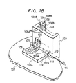
- an integrated circuit region 101A on which various integrated circuits have been constructed is present on a surface of a large-sized semiconductor substrate 101 made of a semiconductor wafer.
- a rectangular opening 102 which has been formed by, for instance, etching treatment, is formed.
- the semiconductor substrate 101 is supported by an upper supporting member 105A and a lower supporting member 105B made of, e.g., an epoxy resin in such a manner that, a rectangular pillar 102 made of, for instance, an alminium alloy or a plastic resin is pierced through the opening 102, and the substrate is sandwiched by both the upper and lower supporting members 105A and 105B formed on the four sides of the pillar 103.
- the central portion of this pillar 103 is made empty.
- a size of the opening 102 of the substrate 101 is defined under the condition that the pillar 103 can be substantially penetrated through the opening 102 while both the upper and lower supporting members 105A and 105B are bent toward the pillar side.
- the pillar 103 is made of a metal such as aluminium, the surface of the metal pillar is covered with a resin so as to electrically insulate the wiring leads.
- a plurality of connector pins 104 are formed on the bottom of the pillar 103 so as to package the pillar 103 which mounts a plurality of semiconductor substrates 101, on a packaging substrate (not shown).
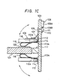
- Both the upper and lower supporting members 105A and 105B have such a shape that, as illustrated in Figs. 1B and 1C, each edge thereof located at the pillar 103 is engaged with a supporting projection 103A which projects from the pillar 103.
- a hole 119 for penetrating a supporting shaft 114 therethrough is formed on the upper supporting member 105A, lower supporting member 105B, and supporting projection 103A, respectively. That is to say, both the upper and lower supporting members 105A and 105B are mounted on the supporting projection 103A in such a manner that they can be rotated with respect to the supporting axis 114 as its rotating center.
- a twist coil spring 112 is arranged on both sides of the upper and lower supporting members 105A and 105B, one end 112A of the twist coil spring 112 is fixed to either the upper supporting member 105A or lower supporting member 105B, and the supporting shaft 114 is penetrated through a central hole 113 thereof. It is seen that only twist coil spring 112 of one edge of the respective upper and lower supporting members 105A and 105B in Figs. 1B and 1C. As a result, the semiconductor substrate 101 is supported by the upper and lower supporting members 105A and 105B by means of the elasticity of the above-described twist coil spring 112.
- a plurality of fixing electrodes are fixed on the upper surface of the upper supporting member 105A, which are made of aluminium on which, for instance, copper or silver is plated.
- a plurality of brush electrodes having elasticity are provided on the side of the pillar 103 corresponding to the fixing electrodes 106, and one end of the respective brush electrodes is resiliently in contact with the surface of the corresponding fixing electrodes 106.
- the end portion of the respective brush electrodes 107 which is resiliently in contact with the respective fixing electrodes, is slidable on the corresponding fixing electrode 106 while the upper supporting members 105A is rotated.
- Another electrode 110 made of, for example, cupper is provided on an inner surface of the pillar 103, in relation to the above-described brush electrode 107, and is connected to the brush electrode 107 by a lead 109 made of, for instance, aluminium on which silver is plated. Between this lead 109 and the pillar 103, an epoxy resin is provided for electrical in sulation.
- the insulated cable 108 is attached to the pillar 103 by adhesive agent so that these insulated cables are employed to connect between the respective semiconductor substrates 101 provided on the pillar 103 and also the semiconductor substrate 101 and the connector pin 104 shown in Fig. 1A.
- a spring electrode 115 having elasticity is provided on the upper surface corresponding to the respective fixing electrodes 106 of the upper supporting member 105A.
- a pin 116 made of, for example, silver-plated aluminium is mechanically and electrically connected between the spring electrode and the fixing electrode 106.
- the respective spring electrodes 115 are resiliently in contact with an electrode 120 made of, for example, an aluminium film which is provided on the surface of the semiconductor substrate 101.
- a spring electrode 115 is provided on the lower supporting member 105B in order that it is used as a supporting member for sandwiching the semiconductor substrate 101. That is to say, the semiconductor substrate 101 is supported in such a manner that a plurality of spring electrodes 115 respectively provided on the upper and lower supporting members 105A and 105B sandwich this substrate 101.
- the upper and lower supporting members 105A and 105B are bent toward the pillar by the manual operation.
- a rubber 117 made of, for instance, a sillicone rubber for preventing the horizontal vibrations is employed between the upper supporting member 105A of the pillar 103 and the lower supporting member 105B.
- the pillar 103 may be shaped as a cylinder according to the invention. In this case, it is apparent that the shape of the opening 102 formed on the semiconductor substrate 101 may be circle.
- both rear surfaces of two sheets of the semiconductor substrates 101, on which no integrated circuit 101A is arranged, are connected to each other by the adhesive agent, and thus the connected semiconductor substrates are sandwiched by these upper and lower supporting members 105A and 105B.
- an interval between the upper and lower supporting members 105A and 105B is wider than that of a single semiconductor substrate 105.
- the packaging device according to the invention may be constructed as packaging device as shown in Fig. 1D.
- the semiconductor substrate 101 has no opening 102 as illustrated in Figs. 1A to 1C.
- the shape of the pillar 103 is formed as a rectanglar pillar or a cylindircal pillar, the upper and lower edges of which are flat surfaces. That is to say, an interior of the pillar 103 is formed as a cavity, and both the upper and lower ends thereof are made closed.
- the adhesive agent 118 is coated on both the upper and lower ends thereof are made closed.
- the adhesive agent 118 is coated on both the upper and lower ends which are in turn attached to the central portion of the semiconductor substrate 101. No integrated circuit is constructed on the portion to which the pillar 103 of the semiconductor substrate 101 is attached.
- Connecting electrodes (not shown) are employed on both surfaces of the semiconductor substrate 101, corresponding to the electrode 115 mounted on the pillar 103. Electrical connection is made between the electrodes formed on both surfaces of the semiconductor substrate 101 via the connecting hole which penetrates through the semiconductor substrate 101.
- the pillar 103 and semiconductor substrate 101 are alternately stacked from the bottom.
- the packaging device for packaging the large-sized semiconductor substrate in a stable condition can be realized.
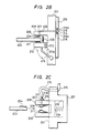
- reference numeral 203 denotes a semiconductor wafer made of a monocrystal silicon and reference numeral 203A indicates an integrated circuit region for constructing various integrated circuits.
- a packaging device of a semiconductor integrated circuit according to the second embodiment includes pillars 201a, 201b, 201c and 201d standing at a peripheral portion of an integrated wafer 203, and a pillar connecting substrate 202 which is connected to the lower end portions of these pillars 201a and 201d so as to stably stand these pillars.
- the pillar 201 and pillar connecting substrate 202 are made of a resin such as an epoxy resin, or aluminium.
- the semiconductor wafer 203 is sandwiched by semiconductor substrate supporting members 205 and 210 which are provided on the pillar 201.
- the pillars for instance, 201b and 201c are arranged to be bent, or brought down as shown in Fig. 2E.
- the remaining pillars 201a and 201d are fixed on the pillar connecting substrate 202.
- only the pillar 201a, three pillars 201a to 201c, or all of the pillars 201a to 201d may be bent or brought down.
- the pillars 201 other than the bendable pillars 201 are fixed on the pillar connecting substrate 202.
- the semiconductor wafer 203 is supported by the upper semiconductor substrate supporting member 205 and the lower semiconductor substrate supporting member 206 mounted on the pillar 201 in the fixed condition.
- the upper semiconductor substrate supporting member 210 is made of, for instance, a resin such as an epoxy resin, or alminium, and is integrally formed with, for example, the pillar 201.
- the lower semiconductor substrate supporting member 210 is mounted on a supporting section 201A projecting from the pillar 201 in such a manner that it is rotatable around the supporting shaft 212.
- the lower semiconductor substrate supporting member 210 is made of, for instance, a resin such as a glass epoxy resin, or aluminium.
- a plurality of hair-pin-shaped spring electrodes 206 are provided on the lower surface of the upper semiconductor substrate supporting member 205 so as to be resiliently connected to the electrode 204 of the semiconductor wafer 203.
- the spring electrode 206 is connected via an embeded wiring lead 207 which penetrates through the upper semiconductor substrate supporting member 205, and the upper wiring lead 208 of the upper surface of the upper semiconductor substrate supporting member 205, to a terminal electrode 214 provided on the outer wall of the pillar 201.
- the wiring lead 208 penetrates through a through hole formed on the pillar 201.
- the hair-pin-shaped pressure spring 211 is provided on the upper surface of the lower semiconductor substrate supporting member 210, i.e., the plane opposite to the semiconductor wafer 203.
- a handle 213 is mounted on the lower surface of the lower semiconductor substrate supporting member 210 so as to open a space defined between the upper and lower semiconductor substrate supporting members 205 and 210 when mounting the semiconductor wafer 203.
- the above-described upper semiconductor substrate supporting member 205, lower semiconductor substrate supporting member 210, and coil spring 209 are mounted on the corresponding pillars 201a, 201b, 201c and 201d, so that the semiconductor wafer 203 can be sandwiched at four positions under the stable condition.
- the above-described spring electrode 206, wiring leads 207 and 208, coil spring 209 and pressure spring 211 are mounted on the respective upper and lower substrate supporting members 205 and 210 which are mounted on the corresponding four pillars 201.
- the electrode 204 is arranged to the semiconductor wafer 203.
- a core 215A of a cable 215 which is insulating-covered with vinyle chloride is connected by solder.
- This insulating cable 215 connects the respective semiconductor wafers 203, and the semiconductor wafers 203 packaged on the packaging substrate and also the wiring lines on the packaging substrate.
- a sandwiching member of the semiconductor wafer 203 is provided in such a manner that the semiconductor wafer supporting, or sandwiching member 205 is ⁇ -shaped, and both the spring electrode 206 and pressure spring 211 are fixed on the side surface of the inside thereof.
- the pillar 201 defines a cavity 218 of a cylindrical form at the portion corresponding to the semiconductor substrate supporting member 205 in order to fit with the semiconductor substrate supporting member 205.
- the semiconductor substrate supporting member 205 fitted within this cavity 218 is positioned to be depressed by the coil spring 219.
- a terminal electrode 217 is provided on the upper surface of the semiconductor substrate supporting member 205, to which the core 215A of the cable 215 is connected.
- the cable 215 extends over the plane opposite to the semiconductor wafer 203, i.e., the outer wall of the pillar 201. This cable 215 is connected via a through hole formed on the pillar 201 adjacent to the semiconductor substrate supporting member 215 to the terminal electrode 216.
- an interval between the spring electrode 206 and pressure spring 211 by which the semiconductor wafer 203 is not yet mounted is narrower than the thickness of the semiconductor wafer 203.
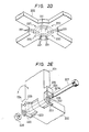
- FIG. 2E One example of the connection between the lower end portion of the pillar 201 and the pillar connecting substrate 202 is shown in Fig. 2E.
- the connecting portion of the pillar connecting substrate 202 is engaged with the lower portion of the pillar 201, and rotatably connected in such a manner that a mounting bolt 227 is inserted into the corresponding bolt hole 230 formed on these portions.
- the bolt 227 is so arranged that it is not dropped from the corresponding bolt hole 230 by mounting a nut 228 on the screw section 227.
- a twist coil spring 222 is positioned on both sides of the pillar and the bolt 227 is penetrated through the respective center holes 226.
- this twist coil spring 222 is mounted in the spring mounting hole 223 of the pillar connecting substrate 202, whereas the other end thereof is mounted in the spring mounting hole 225 formed on the projecting 224 of the pillar 201.
- the pillar 201 can be stood up at a right angle by this twist coil spring 222, and also the bent pillar 201 can be recovered by means of the twist coil spring 222.
- both the pillar 201 and pillar connecting substrate 202 may be constructed as shown in Fig. 2F.
- pillar 201b among four pillars 201 is so arranged to be bent.
- a hinge is mounted between the bent pillar 201b and the pillar connecting substrate 202 at these connecting sections 202A in such a manner that it is mounted between the outer wall of the pillar 201 and the edge portion of the pillar connecting substrate 202. Since the hinge is mounted to the outer wall of the pillar 201b, the pillar is not bent inside, but allowable to be bent outside.
- a lid 229 is employed to cover it.
- the semiconductor substrate supporting members 205 shown in Fig. 2B or 2C and 210 are provided with the pillar 201 illustrated in Fig. 2F.
- Both the rear surfaces of the semiconductor wafer 203, for instance, are attached to each other, and the resultant semiconductor wafers 203 may be supported by either the semiconductor substrate supporting members 205 and 210 (see Fig. 2B), or 205 (Fig. 2C).
- the interval between the semiconductor supporting members 205, 210, and 205, into which the semiconductor wafer 203 can be inserted is made wider than that of the single semiconductor wafer 203.
- the semiconductor wafer 203 is not limited to the above-mentioned wafer, but may be such a semiconductor substrate that, for example, the peripherals of the semiconductor wafer 203 are cut off to form a rectangle-shaped semiconductor wafer.
- the layout for arranging the respective pillars 201, and the size and shape of the pillar connecting substrate 202 may be modified, depending upon the size and shape of the employed semiconductor substrate.
- the packaging device is constructed of a plurality of pillars standing around the peripherals of the semiconductor wafer, the semiconductor substrate supporting members and pillar connecting members and pillar connecting substrate mounted thereto, the semiconductor wafer can be supported thereon without any twist and vibration phenomenon. As a consequence, a large-sized semiconductor integrated circuit constructed of a semiconductor wafer can be packaged under the stable condition.
- the semiconductor device according to the third embodiment is so arranged in that a plurality of semiconductor chips "Chip” made of a single crystal silicon are mounted on a mounting substrate 301 made of a single-crystal semiconductor wafer. Between the respective semiconductor chips "Chip”, there are provided a wiring region 303 consisting of a wiring line 304x made of an aluminium film as a first layer for connecting the semiconductor chips "Chip”, and also a wiring line 304y made of an aluminium film as a second layer. These first and second layers 304x and 304y extend in the wiring region 303.
- the wiring line 304x of the first layer extend over an insulating film 308 of a silicon oxide film which is formed on the mounting substrate 301 by, for instance, the CVD method.
- An insulating film 309 made of a silicon oxide film by, for instance, the CVD method is employed to inslate between the wiring line 304x and the wiring line 304y of the second layer.
- a final protection film 310 made of a silicon oxide film which is processed by, for example, the CVD method, covers the wiring line 304y.
- the connection between the wiring line 304x and wiring line 304y is accomplished by a connecting hole which is formed by removing the insulating film 309.
- a plurality of bonding pads which are constructed by stacking the aluminium film 302x of the first layer and the aluminium film 302y of the second layer.
- the aluminium film 302x is overlaid on the insulating film 308, whereas another aluminium film 302y is connected to the aluminium wiring line 302x via a connecting hole 311 which is formed by removing the insulating film 309.
- Either the above-described wiring line 304x or 304y is connected to the bonding pads 302.
- this wiring line 304x is integrally formed with the aluminium film 302x which constitutes the lower portion of the bonding pad 302.
- this wiring line 304y is integrally formed with the aluminium film 302y which constitutes the upper portion of the bonding pad 302.
- the final protection film 310 has been removed when overlaying the bonding pad 302, and then becomes an opening 312.
- a plurality of bonding pads 305 formed by stacking the aluminium layer 305x of the first layer and the aluminium layer 305y of the second layer.
- the aluminium film 305x is located over the insulating film 308.
- the aluminium film 305y is connected via the connecting hole 311 to another aluminium film 305x.
- the bonding pad 305 is exposed from the opening 312.
- Either wiring line 304x or wiring line 304y is connected to the bonding pad 305.
- the aluminium film 305 constituting the lower portion of this bonding pad 305 is integrally formed with the wiring line 304x.
- the aluminium layer 305y constituting the upper portion of this bonding pad 305 is integrally formed with the wiring line 304y.
- no element such as MISFET, bipolar transistor, resistor element, capacitive element and so on is constructed.
- resistor element or capactive element may be formed on the portion other than the region on which the semiconductor chips "Chip" are mounted in the surface portion of the mounting substrate 301.
- the semiconductor chips "Chip” are attached on the final protection film 310 by means of an adhesive agent 313 such as a sillicone rubber. Stress applied to the semiconductor chips “Chip” can be reduced by introducing the sillicone rubber into the adhesive agent.
- a plurality of bonding pads 307 are arranged around the peripheral of the semiconductor chips “Chip”. This bonding pad 307 is so constructed by stacking up, for instance, the aluminium film of the first layer and the aluminium film of the second layer. It should be noted that a large quantity of MISFET, bipolar transistor, resistor element and capacitive element are provided on the surface of the semiconductor chips "Chip".
- a field insulating film made of a silicon oxide film is formed by way of, for instance, thermal oxidation.
- wiring lines made of a poly-crystal silicon film formed by the CVD method (treatment), or an aluminium film formed by the sputtering treatment are extended.
- An insulating film made of a silicon oxide film formed by, for example, the CVD treatment is employed to made an electrical insulation between the upper wiring line and the lower wiring line.
- an insulating film of a first layer which is made of a silicon oxide film formed by, for instance, the CVD method, and covers, for example the MISFET's gate electrode.
- the upper portions of the semiconductor chips "ChiP" are covered with a final protection film 314 which is formed by stacking a silicon oxide film, and a coating glass (SOG) film by way of the CVD method, or a silicon nitride film by way of the sputtering treatment.
- This final protection film 314 has been selectively removed on the bonding pad 307 so that it becomes an opening 315.
- a bonding wire is connected, which is made of an aluminium wire on which, for instance, a gold wire and a silver wire have been plated.
- the connection between the bonding wire 306 and the bonding pad 307, and also the bonding wire 306 and the bonding pad 305, is performed by means of, for instance, the ultrasonic bonding, thermal contacting and so on.
- This bonding wire 316 is connected to a lead 320 made of a 42 alloy, as illustrated in Fig. 3D.
- Fig. 3D there is shown a sectional view of the mounting substrate 301, the package substrate 318A for sealing the semiconductor chips "Chip” and the package cap 318B.
- the packaging substrate 318A is made of, for instance, ceramics, and alumina etc.
- the package cap 318B is made of, for example, ceramics.
- the mounting substrate 301 is attached to the packaging cap 318A by means of the adhesive agent 317 made of, for instance, a sillicone rubber. By employing the sillicone rubber into the adhesive agent 317, stress applied to the mounting substrate 301 made of a single crystal silicon can be reduced.
- the packaging substrate 318A is attached to the package cap 318B by means of a sealing agent 319 made of, for instance, glass. A gap between the packaging substrate 318A and the packaging cap 318B formed by a lead 320 is sealed by the sealing agent 319.
- the adhersive connection between the semiconductor chips “Chip” and the mounting substrate 301 may be accomplished in such a manner that the insulating films 308 and 309 underneath the semiconductor chips “Chip”, and the final protection film 310 are selectively removed to expose the surface of the mounting substrate 301, and these semiconductor chips “ChiP" are connected to the exposed region by means of the adhesive agent 313.
- the adhesive connection between the semiconductor chips "ChiP" and the mounting substrate 301 may be accomplished by employing, for example, an Au paste.
- the electrical connection between the semiconductor chips "Chip” and the mounting substrate 301 is performed by employing the bonding pad 307, bonding wire 306 and bonding pad 305, the reliability on the electrical connection between the semiconductor chips "Chip” and the mounting substrate 301 can be improved due to the fact that the rigid connection between these parts is established.
- the heat produced in the semiconductor chips "Chip” can be radiated via the mounting substrate 301 to the packaging substrate 318A,and furthermore to the atmosphere. This implies that the higher heat radiation effect can be realized because the semiconductor chips "Chip” are not separated from the mounting substrate 301. This effect can be specifically improved in such a semiconductor device where a plurality of semiconductor chips "Chip” are sealed within the same package (318A, 318B).
- the mounting substrate 301 is made of the same material, i.e., single crystal silicon as that of the semiconductor chips "Chip", a difference in the thermal expansion between these elements can be reduced to zero.
- the mounting substrate 301 is used as the semiconductor wafer, no the stress concentration onto the mounting substrate 301 is introduced so that no damage is made in the mounting substrate 301, which can improve the reliability.
- the mounting substrate 301 is not made from the semiconductor wafer, but may be formed as a rectangular mounting substrate 301, the peripheral portions of which are cut off.
- the semiconductor integrated circuit device may be built within an IC card.
- the size of the mounting substrate 301 is made small enough to store the mounting substrate 301 within the IC card, so that a plurality of semiconductor chips "Chip" are mounted thereon.
- the bonding wire 306, and the bonding pads 307 and 305 are employed to connect between this semiconductor chip "Chip” and the mounting substrate 301.
- the semiconductor integrated circuit device is not sealed in the package substrates 318A and 318B, but stored in the IC card.
- the bonding wire is employed to connect between the semiconductor chip and the mounting substrate, the reliability on the electrical connection between the semiconductor chip and the mounting substrate can be improved.
- the heat generated in the semiconductor chip can be radiated via the mounting substrate to the package, and in turn in the atmosphere. In other words, the radiation effect can be improved.
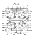
- FIG. 4A there is shown a block diagram of a fourth embodiment in which the present invention is applied to a wafer-scale semiconductor memory device.
- Each of the circuit blocks shown in Fig. 4A is formed based upon the known manufacturing technique for a semiconductor integrated circuit.
- Each of the circuit blocks shown in Fig. 4A is drawn, taking account of the practical geometric circuit arrangement on a wafer-scale WSI (wafer-scale semiconductor integrated circuit device).
- the memory blocks M0 to M29 are not specifically limited, but are constructed of memory arrays constituting dynamic type RAM's, and also decoder circuits for performing their selecting operation. That is to say, as shown in Fig. 4B, the memory block Mi is, briefly speaking, constructed of a memory array, a column decoder CDCR for selecting its data line (bit line, or digit line), and a row decoder RDCR for selecting its word line. As represented by a dotted line in Fig. 4A, the memory array is subdivided into two memory mats, in principle. A sense amplifier SA is arranged on each center portion of the respective memory mats.
- a switch circuit may be employed for selectively connecting this sense amplifier to either memory mat (not shown in detail).
- a column switch circuit may be provided in parallel to this sense amplifier.
- the above-described memory block Mi includes various circuits (not shown in detail). These arrangements of the memory array and the address selecting circuit may be constructed of the circuit equivalent to the known dynamic type RAM. In the preferred embodiment, the memory array is also subdivided vertically to obtain two divided portions as illustrated in Fig. 4, for the sake of convenience.
- the above-described memory blocks M0 to M29 require a relatively large rectangular area to be occupied. Accordingly, an empty space is produced around the peripheral portion of a substantially circular wafer WSI.
- the above-described preliminary memory circuit RM is so designed as to occupy a relative smaller area where there are a memory array section corresponding to the memory mats subdivided from one memory block, and a decoder circuit thereof.
- a large quantity of the above-described preliminary memory circuits RM are formed at the peripheral portion of the wafer on which the memory block Mi required to have the relatively large occupied area can be formed.
- Such a circuit arrangement can prevent the practical memory capacity from being reduced when adding the redundant circuit. In other words, while adding the redundant functions, the memory system owning the larger memory capacity can be obtained.
- a control circuit CONT may be arranged at a position corresponding to an orientation flat section of the wafer WSI.
- This control circuit CONT performs the selection operation of the above-described memory block Mi by receiving address signals BA and MA and a control signal TC supplied from the external source.
- an electrode to be connected to the above external terminal is provided on the above-described orientation flat section. This electrode is utilized for the probing when the memory system constituted by the above-described memory block circuit RM and also control circuit CONT formed on the wafer WSI is accomplished.
- the address signal BA among the above-described address signals corresponds to a block address signal for designating one memory blocks M0 to M29.
- the address signal MA corresponds to an address signal commonly supplied to the above-described respective memory blocks M0 to M29. Therefore, the control circuit CONT includes a decoder circuit for producing a selection signal for one memory block, while receiving the above-described block address signal BA. Between the above-described control circuit CONT and the respective memory blocks M0 to M29, there are arranged an address supply line for supplying the above-described common address signal MA, a signal line for supplying and receiving a read/write signal between the respective memory blocks M0 to M29, a timing signal for controlling various operations, and a selecting signal line formed by decoding the above-described block address signal BA. Due to complex circuitry, such signal lines are omitted in the figures.
- an address supply line for supplying an address signal with respect to the above-described preliminary memory circuit RM, a signal line for receiving/supplying a read/write signal between the respective preliminary memory circuits RM, and a signal line for the same timing signal and selection signal as in the above case,
- the preliminary memory circuit RM has only 1/4 memory capacity, as compared with the memory capacity of one ememory block Mi, the addredd setting operation and also the allocation of the selecting signal line can be performed by a program.
- the address signal except for the respective most significant bits of the row/column with respect to the above-described memory block Mi, is supplied to the respective decoder circuits.
- the selection signal line for the respective preliminary memory circuits RM is provided in one-to-one correspondence with the control circuit CONT. This selecting signal line is designated by combining the block address signal designated under control of the control circuit CONT with the remaining higher 2-bit address signal. As a consequence, one preliminary memory circuit RM is allocated to the address block and the higher 2-bit memory address by the address designation at the control circuit CONT.
- control circuit CONT performs the memory access with respect to the respective memory blocks M0 to M29 and owns such a function that while judging whether or not the defect is present, it sends out externally a failed address signal NA(block address) corresponding to the failed memory block.
- the operation per se of the above-described memory system is similar to that of the conventional board-arranged memory device wherein the memory block is constructed of one semiconductor integrated circuit device, and the wafer WSI is substituted by a printed substrate.
- the block addresses are allocated to the respective memory blocks.
- the memory block Mi essentially containing such a defect can be separated by invalidate the corresponding selection signal.
- the power supply line should be separated by projecting the laser ray, as similarly in the conventional system.
- the above-described defect relieving can be relatively simply performed.
- the defect occurs in one word line at the memory block and the data line connected to the memory cell, similarly the failed address NA is output, so that the program for relieving a defect can be made readily.
- the above-described defect relieving operation by employing the above-described preliminary memory circuit RM is performed every memory block according to the most simple way. That is to say, the selection is prohibited by cutting off, for instance, fuse means with respect to the memory block containing the defect. Then, the block address is stored in the memory circuit which utilizes the fuse means, when the memory address corresponding to the block address is detected, one memory block is constructed by four preliminary memory circuits RM, and thereafter this memory block is selected.
- Such a selection for the redundant circuit can be accomplished by utilizing the defect releiving technique which is performed at the word line or data line unit in the conventional dynamic type RAM.
- the selection for the defective memory mat is detected while the remaining three memory mats remain alive, so that the selection is carried out for the above-described preliminary memory circuit.
- the defective, or failed address is designated in the control circuit CONT as the defective, or failed address based upon the block address and the respective 1-bit most significant bit of the row system and column system, in other words, the 2-bit address signal for designating one memory mat among the subdivided four memory mats MAT.
- the supply of the selection signal for its memory block is prohibited, and the corresponding preliminary memory circuit RM is selected. In this case, since each of these preliminary memory circuits RM can be independently used, the redundancy can be increased.
- the memory block may be constructed of the above-described dynamic type RAM, but also a static type RAM. Moreover, it may be possible to simultaneously employ a dynamic type RAM, static type RAM and mask ROM.
- circuit blocks having the specific circuit function not only the above-described memory blocks, but also a peripheral circuit constituting a microcomputer system may be utilized.
- the circuit block containing the defect can be essentially separated from the system by allocating the above-described block address.
- the present invention can be widely applied to a VLSI which is constructed of a wafer-scale substrate.
- the system can be built up on the wafer by comprising a plurality of circuit blocks having the specific circuit functions, and allocating the block address to designate the respective circuit blocks. Therefore, it is possible to perform the function test for the respective circuit blocks by designating the block address. Also by employing the above-defined block address, the defective, or fault circuit block can be practically cut out from the main circuit block. As a consequence, the conventional steps for cutting off the wiring line by irradiating the laser beams time to time, and for wiring the effective circuit blocks can be omitted.
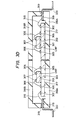
- an electron beam is first irradiated to a substrate 501 such as a silicon substrate, so that a large quantity of fine through holes having, for example, a diameter of 100 ⁇ m are formed thereon.
- This electron beam irradiation can be performed by employing, for instance, an electron-beam direct exposure apparatus having a large-sized electron gun.
- these through holes 501a can be formed at the very precise positioning.
- an input/output pin 509 see Fig. 5D
- an input/output pin 509 can be arranged in high density (will be described later).
- a multi-pin arrangement can be realized.
- an ion beam may be employed instead of the above electron beam.
- the above-described semiconductor substrate 501 is thermally oxidized so as to form an insulating fim 502 such as a SiO2 film over the entire surface including the inner peripheral surface of the through hole 501a.
- the above-described semiconductor sub strate 501 is stored in a reaction tube 503 of a CVD apparatus as illustrated in, for example, Fig. 5E. While this semiconductor substrate 501 is heated to a predetermined temperature, both, for instance, tungsten hexafluoride (WF6) and hydrogen (H2) are flown from one end portion of this reaction tube 503 toward the semiconductor substrate 501 in the vertical direction. Then, the gas phase reaction expressed by the following formula is carried out: WF6 + 3H2 ⁇ W + 6HF During the reaction step, the above-described reaction gas flows through the through hole 501a of the semiconductor substrate 501. Since, as shown in Fig.
- tungsten (W) is deposited which is produced in this gas phase reaction, the interior of the through hole 501a is filled with tungsten, and then, the connecting wire 504 can be formed which is insulated by the insulating film 502 from semiconductor substrate 501. It should be noted that since tungsten is practically deposited not only on the through hole 501a, but also the surface of the insulating film 502 during the gas reaction, both surfaces of the semiconductor substrate 501 are polished to remove the unnecessary tungsten deposition after depositing tungsten.
- Fig. 5C illustrates the condition after polishing the substrate.
- Fig. 5D illustrates a so-called multi-chip module where the semiconductor substrate 501 thus formed is utilized as the packaging substrate.
- a multi-layer wiring line 506 made of, for example, an aluminium wiring line is formed on the above-described semiconductor substrate 501 by insulating the respective layer wiring lines by employing an insulating material such as a polyimide resin.
- a solder bamp 507 is formed at one end portion of this multi-layer wiring line 506, for example.
- a plurality of LSI chips 508 such as silicon chips are packaged via this solder bump 507.
- solder bump 507 is connected to the bonding pad (not shown) provided on the LSI chip 508.
- This LSI chip 508 is connected to the input/output pin 509 by means of the above-described multi-layer wiring line 506 and connecting wire 504.
- both the packaging substrate constructed of the semiconductor substrate 501 and the LSI chips 508 are made of the same material (e.g., silicon), there is no difference in the thermal expansion coefficient between the packaging substrate and the LSI chips 508. Consequently, it is possible to prevent occurrence of thermal stress at the solder bump section 507 due to this difference of the thermal expansion coefficient. As a result, a temperature cycle life can be improved and also the large-sized LSI chip can be utilized.
- tungsten was employed as the metal for constructing the connecting wire 504 in the above-described preferred embodiment, it is of course possible to use other materials such as M0 and Al.
- these metals may be formed by way of the methods other than the CVD method, e.g., the nonelectrolyte method.
- the packaging substrate where the metal for constituting the connecting wire is filled with the fine through holes which have been formed at higher positioning precision.
Abstract
Description
- The present invention relates to the packaging of semiconductor integrated circuits, and more particularly to a packaging technique for semiconductor integrated circuits formed on a large-sized semiconductor substrate such as a semiconductor wafer.
- In general, semiconductor integrated circuits are constructed on respective parts of a substate, i.e. a semiconductor wafer chip the wafer then being subdivided by dicing it into a plurality of parts each corresponding to one or more integrated circuits. However, recently, constructions have been investigated in which the semiconductor wafer is not subdivided, but a plurality of integrated circuits are fabricated on the whole of the semiconductor wafer so as to construct a large-sized semiconductor integrated circuit. Such a semiconductor manufacturing technique is described in e.g. Japanese patent KOKAI (Disclosure) 61-290739, in which one large-sized semiconductor integrated circuit is constructed on the entire semiconductor wafer.
- There is, however, no known method of packaging a large-sized semiconductor wafer. To overcome this problem, the present invention proposes a packaging device which engages such wafer(s) and thereby holds them in place.
- When several such wafers are mounted on the packaging device, the device can then hold the wafers in a spaced-apart relationship.
- In one alternative the present invention proposes that the packaging device support the wafer(s) at a central part thereof. This has the advantage that the wafer(s) are stably supported. Such central support may be achieved by forming the packaging device into a plurality of sections which are attached to the centre of each wafer and extend between one wafer and the adjacent wafer. However, it is preferred that each substrate has an opening at a central part thereof, and the packaging device comprises an elongate pillar extending through those openings and engaging each substrate at or adjacent the opening.
- In another alternative the packaging device comprises a plurality of interconnected pillars each having means for engaging the substrates at the periphery of those substrates. This has the advantage that the wafer(s) are supported at a plurality of positions, so that the wafer(s) cannot vibrate or twist. The pillars may then be hingedly interconnected to the base, possibly via springs which holds them into engagement with the wafers.
- Thus, the present invention, in a first aspect, may provide a stack of large-sized semiconductor substrates, comprising a packaging device engaging the substrates to maintain them in a spaced apart relationship.
- The wafer(s) may then be electrically connected to the packaging device, e.g. by spring electrodes.
- The applicants have also investigated the problems which occur when a plurality of semiconductor chips are mounted on a mounting substrate (mother chip), and are then sealed. To achieve higher package density of semiconductor chips, a plurality of semiconductor chips are thus stored into a single package. Each of the semiconductor chips stored within the package is mounted on a mother chip. Aluminium wiring lines extend over the mother chip to interconnect the semiconductor chips. The aluminium wiring lines and the semiconductor chips are connected by bump electrodes made of e.g. gold (Au), or solder. For instance, a conventional semiconductor device where a plurality of semiconductor chips are mounted on a single package is described in Japanese patent KOKAI (Disclosure) application No. 60-198758.
- The underlaying film made of tungsten and titanium is formed between the aluminium wiring leads and gold or solder for constituting the above-described bump electrodes. This is because gold or solder is easily removed from the silicon oxide film which covers the aluminium film. However, adhesion between gold or solder, and tungsten or titanium functioning as an underlayer is relatively weaker than that between the bonding wires made of an aluminium film or gold, and the bonding pads made of an aluminium film, so that the gold or solder tends to be removed from the underlayer. As a consequence, the semiconductor chips are readily removed from the mother chip.
- Since the bump electrode is present between the semiconductor chip and the mother chip, a gap may thus be established between the semiconductor chip and the mother chip, which causes the efficiency of heat radiation to be lowered. This problem is particularly significant in that the temperature of a semiconductor package may be increased considerably if a plurality of semiconductor chips are provided within the same package.
- Therefore, in another aspect, the present invention seeks to improve the reliability of connection between the semiconductor chip and the mounting substrate, and possibly to increase the heat radiation effect of the semiconductor device where a plurality of semiconductor chips are built.
- The second aspect of the present invention proposes that this problem be solved, or at least ameliorated, by interconnecting the bonding wire between the semiconductor chip and the wiring lines formed on the substrate on which the above-described semiconductor chip is mounted.
- Since according to this aspect of the present invention, the connection between the bonding pad provided on the semiconductor chip and the bonding wire thereof, and also the connection between the bonding wire and the bonding pad provided on the mounting substrate are made rigid, the reliability of the interconnection between the semiconductor chip and the substrate on which this semiconductor chip is mounted can be improved.
- As, moreover, the rear surface of the semiconductor chip may be attached to the mounting substrate, the radiation effect of the heat produced from the semiconductor chip can be improved.
- Thus, according to this second aspect of the present invention there may be provided a packaging device for a semiconductor integrated circuit wherein in a semiconductor device where a plurality of semiconductor chips are mounted on a mounting substrate, and a wiring line is extended over the mounting substrate so as to electrically connect said semiconductor chips with each other, a bonding wire is employed to make a connection between said semiconductor chip and the wiring line provided on the mounting substrate.
- Preferably, both the semiconductor chips and the mounting substrate may be sealed within the same package. Furthermore, the surface of the semiconductor chip which is opposite to that on which the bonding pad is located may be attached to the mounting substrate.
- A semiconductor memory device fabricated by a wafer-sized very LSI has been proposed from, for instance Japanese patent KOKAI (Disclosure) application No. 59-201441. In the wafer-sized semiconductor memory device described as in the above disclosure, the cutting of the defective chips and removal of these defective chips are performed by such a way that fuses, or power source lines are cut out by irradiating focused ion beams, or laser light rays, and only those chips without defects are connected by the final wiring. However, a large number of manufacturing stages and thus, a large number of masks are required. As a result, the throughput is not improved and the cost is high. Moreover, one or more redundant blocks for removing the defects is built in the memory system body within the wafer so that to increase the redundancy, the total area which the entire system body occupies must be reduced. If a faulty block is to be discovered by means of probing, the lower throughput must be accepted. In some cases, such a probing check may cause another defect.
- Therefore, in a third aspect, the present invention seeks to provide a wafer-sized semiconductor integrated circuit device which permits a more satisfactory defect relieving method.
- To achieve this, the third aspect of the present invention proposes that a semiconductor integrated circuit device has a plurality of circuit blocks having specific circuit functions, whereby the block addresses are allocated so as to designate the respective circuit blocks.
- Since, according to this aspect of the invention, the system is built up on the wafer, a test to check the functioning of an individual circuit block can be carried out separately by the designation of the above-described block address. As a consequence, the cutting of the defective block can be essentially achieved by employing the above-described block address.
- Thus, according to this third aspect of the invention there may be provided a wafer-scale semiconductor integrated circuit device comprising a plurality of circuit blocks each having a specific circuit function, whereby a block address for designating the respective circuit blocks is allocated.
- Then, a plurality of semiconductor memory circuits may be provided, including a decoder circuit as the circuit block and a memory array selected by the decoder circuit. A control circuit may then be allocated to the respective semiconductor memory circuits, which performs a selection operation based on the block address.
- Preferably, the selection operation in the semiconductor memory circuit is prohibited by the block address due to existence of a defect.
- The wafer-scale integrated circuit device may be constructed of a plurality of memory mats, a memory array section of the semiconductor memory circuit being subdivided. Then, a preliminary memory circuit having a decoder circuit corresponding to the memory mat is arranged around a peripheral section of a wafer, and when a defect is present, the selection of the preliminary memory circuit is performed, and the selection of the semiconductor circuit is prohibited.
- It is desirable that the control circuit functions to output externally the block address of the semiconductor substrate containing the defect.
- A fourth aspect of the present invention is concerned with a method of manufacturing a packaging substrate. It is known to provide a chip carrier type package as a package suitable for higher packaging density of LSI (known from, for instance, "VLSI Device Handbook", issued on November 28, 1983,
pages 226 to 228 by Science Forum). The so-called "alumina green sheet (non-sintered alumina sheet)" is most commonly utilized as the material of the packaging substrate employed for packaging the LSI in accordance with the above chip carrier method (for example, described on pages 239 to 242 of that handbook). When forming the packaging substrate by employing this green sheet, through holes are formed by photo-lithography and etching techniques which are commonly utilized for fabricating an LSI. Then, for example, W-paste is printed to fill these through holes with W-paste, and finally the green sheet is sintered. - However, the applicants have become aware of the following difficulty of the conventional technique. Since, the interval between the successive through holes has a different value before and after sintering, due to the shrinkage of the green sheet which is sintered, the precision of the positioning of the through hole is not high. As a result, there is a drawback in the alignment process of the photo-lithography step for forming on the above-described green sheet, the connecting wire made of the W-paste filled in this through hole and the wire to be connected.
- A fourth aspect of the present invention seeks to overcome this problem. It proposes that:
the through hole is formed by irradiating the beam to the semiconductor substrate;
the insulating film is formed of the surface of the semiconductor substrate by thermal-oxidizing the semiconductor substrate; and
the metal is filled into the interior of the through hole. - Since, according to this aspect of the invention, the through hole is formed by beam irradiation, a fine through hole can be formed with the higher positioning precision, and also the connection wire can be formed by filling the metal into this through hole.
- Preferably, the beam is either an electron beam or an ion beam. CVD may be used to fill the through hole with metal.
- Embodiments of the present inention will now be described in detail, by way of example, with reference to the accompanying drawings, in which:
- Fig. 1A is a perspective view of an entire packaging device for supporting a plurality of large-sized semiconductor substrates constructed of a semiconductor wafer;
- Fig. 1B is an enlarged perspective view of a supporting member employed in the packaging device shown in Fig. 1A;
- Fig. 1C is a side view of the supporting member;
- Fig. 1D is a side view of the modified supporting member;
- Fig. 2A is a perspective view of an entire packaging device;
- Figs. 2B and 2C are side views of a semiconductor substrate supporting member;
- Fig. 2D is a perspective view of a pillar connecting substrate 2, which is observed from its bottom side;
- Fig. 2E is a perspective view of a connection part between the pillar and the pillar connecting substrate;
- Fig. 2F is a perspective view of a modified packaging device;
- Fig. 3A is a plan view of a mounting substrate on which a plurality of semiconductor chips are mounted;
- Fig. 3B is a plan view of a portion of the mounting substrate;
- Fig. 3C is a sectional view of the semiconductor chip, taken along the line passing therethrough, on the mounting substrate;
- Fig. 3D is a sectional view of a package for sealing the mounting substrate;
- Fig. 4A is a schematic block diagram of a memory system, according to one preferred embodiment, to which the present invention is applied;
- Fig. 4B is a schematic block diagram of the memory block according to a preferred embodiment;
- Figs. 5A to 5C are sectional views for explaining a manufacturing method of the packaging substrate in the order of the manufacturing step;
- Figs. 5D is a sectional view for indicating a multi-chip module which packages an LSI chip by employing the packaging substrate that is manufactured according to the manufacturing method of the packaging substrate, as illustrated in Figs. 5A to 5C; and
- Fig. 5E is a method for forming the connecting wire based upon CVD method with respect to the method for manufacturing the packaging substrate, as illustrated in Figs. 5A to 5C.
- In a semiconductor integrated circuit according to the present invention, as illustrated in Fig. 1A, an
integrated circuit region 101A on which various integrated circuits have been constructed, is present on a surface of a large-sized semiconductor substrate 101 made of a semiconductor wafer. At a central portion of the above-describedsemiconductor substrate 101, arectangular opening 102 which has been formed by, for instance, etching treatment, is formed. Thesemiconductor substrate 101 is supported by an upper supportingmember 105A and a lower supportingmember 105B made of, e.g., an epoxy resin in such a manner that, arectangular pillar 102 made of, for instance, an alminium alloy or a plastic resin is pierced through theopening 102, and the substrate is sandwiched by both the upper and lower supportingmembers pillar 103. The central portion of thispillar 103 is made empty. A size of theopening 102 of thesubstrate 101 is defined under the condition that thepillar 103 can be substantially penetrated through theopening 102 while both the upper and lower supportingmembers pillar 103 is made of a metal such as aluminium, the surface of the metal pillar is covered with a resin so as to electrically insulate the wiring leads. A plurality of connector pins 104 are formed on the bottom of thepillar 103 so as to package thepillar 103 which mounts a plurality ofsemiconductor substrates 101, on a packaging substrate (not shown). - Both the upper and lower supporting
members pillar 103 is engaged with a supportingprojection 103A which projects from thepillar 103. Ahole 119 for penetrating a supportingshaft 114 therethrough is formed on the upper supportingmember 105A, lower supportingmember 105B, and supportingprojection 103A, respectively. That is to say, both the upper and lower supportingmembers projection 103A in such a manner that they can be rotated with respect to the supportingaxis 114 as its rotating center. To sandwich thesemiconductor substrate 101 by the upper and lower supportingmembers twist coil spring 112 is arranged on both sides of the upper and lower supportingmembers end 112A of thetwist coil spring 112 is fixed to either the upper supportingmember 105A or lower supportingmember 105B, and the supportingshaft 114 is penetrated through acentral hole 113 thereof. It is seen that onlytwist coil spring 112 of one edge of the respective upper and lower supportingmembers semiconductor substrate 101 is supported by the upper and lower supportingmembers twist coil spring 112. - A plurality of fixing electrodes are fixed on the upper surface of the upper supporting
member 105A, which are made of aluminium on which, for instance, copper or silver is plated. A plurality of brush electrodes having elasticity are provided on the side of thepillar 103 corresponding to the fixingelectrodes 106, and one end of the respective brush electrodes is resiliently in contact with the surface of the corresponding fixingelectrodes 106. The end portion of therespective brush electrodes 107 which is resiliently in contact with the respective fixing electrodes, is slidable on the corresponding fixingelectrode 106 while the upper supportingmembers 105A is rotated. Anotherelectrode 110 made of, for example, cupper is provided on an inner surface of thepillar 103, in relation to the above-describedbrush electrode 107, and is connected to thebrush electrode 107 by a lead 109 made of, for instance, aluminium on which silver is plated. Between thislead 109 and thepillar 103, an epoxy resin is provided for electrical in sulation. A core 108B of an electrically insulatedcable 108, the surface of which is covered with an insulatingfilm 108A such as a resin, vinyl chloride, is connected to thecorresponding electrode 110 by, for example,solder 111. Theinsulated cable 108 is attached to thepillar 103 by adhesive agent so that these insulated cables are employed to connect between therespective semiconductor substrates 101 provided on thepillar 103 and also thesemiconductor substrate 101 and theconnector pin 104 shown in Fig. 1A. - A
spring electrode 115 having elasticity is provided on the upper surface corresponding to therespective fixing electrodes 106 of the upper supportingmember 105A. Apin 116 made of, for example, silver-plated aluminium is mechanically and electrically connected between the spring electrode and the fixingelectrode 106. Therespective spring electrodes 115 are resiliently in contact with anelectrode 120 made of, for example, an aluminium film which is provided on the surface of thesemiconductor substrate 101. Also, aspring electrode 115 is provided on the lower supportingmember 105B in order that it is used as a supporting member for sandwiching thesemiconductor substrate 101. That is to say, thesemiconductor substrate 101 is supported in such a manner that a plurality ofspring electrodes 115 respectively provided on the upper and lower supportingmembers substrate 101. - When the
semiconductor substrate 101 is loaded on thepillar 103, as illustrated in Fig. 1C, the upper and lower supportingmembers semiconductor substrate 101, which is supported by both the upper and lower supportingmembers rubber 117 made of, for instance, a sillicone rubber for preventing the horizontal vibrations is employed between the upper supportingmember 105A of thepillar 103 and the lower supportingmember 105B. - It should be noted that the
pillar 103 may be shaped as a cylinder according to the invention. In this case, it is apparent that the shape of theopening 102 formed on thesemiconductor substrate 101 may be circle. - It should also be noted that both rear surfaces of two sheets of the
semiconductor substrates 101, on which nointegrated circuit 101A is arranged, are connected to each other by the adhesive agent, and thus the connected semiconductor substrates are sandwiched by these upper and lower supportingmembers members single semiconductor substrate 105. - The following effects according to the first embodiment will be achieved.
- (1). The packaging device according to the first embodiment is so constructed that the center portion of the above-described
semiconductor substrate 101 is supported by thepillar 103 which passes through the center portion of the large-sized semiconductor substrate 101, and also by the upper and lower supportingmembers pillar 103. Accordingly, since the large-sized semiconductor substrate 101 can be supported in a stable condition, the packaging device for stably packaging thesemiconductor substrate 101 can be obtained. - (2). Since the
spring electrodes 115 are provided on the upper and lower supportingmembers semiconductor substrate 101, thesemiconductor substrate 101 can be supported and simultaneously, the electrical connection can be established between therespective semiconductor substrates 101, and also between thesemiconductor substrate 101 and the packaging substrate. - (3). As the
connector pin 104 is mounted on the bottom of thepillar 103, thepillar 103 is packaged onto the packaging substrate and simultaneously, the electrical connection can be achieved. - (4). Since the center portion of the
semiconductor substrate 101 is connected to thepillar 103, the maximum distance between this connection point and the arbitrary point on thecircuit region 101A is substantially equal to a half of the diameter of thesemiconductor wafer 101 so that a difference between the transferring speeds can be reduced. - (5). As the center portion of the
semiconductor substrate 101 is supported, and no shielding part is present around the semiconductor substrate, the heat radiation effect can be improved. - (6). Since a plurality of
semiconductor substrates 101 are mounted on thepillar 103 in such a way that these substrates are successively overlapped along thepillar 103, a large quantity of circuits can be arranged within a smaller packaging area. - While the present invention has been described using a specific embodiment, it should be understood that further modifications and changes can be made without departing from the scope of the present invention.
- For instance, the packaging device according to the invention may be constructed as packaging device as shown in Fig. 1D.
- In Fig. 1D, the
semiconductor substrate 101 has noopening 102 as illustrated in Figs. 1A to 1C. The shape of thepillar 103 is formed as a rectanglar pillar or a cylindircal pillar, the upper and lower edges of which are flat surfaces. That is to say, an interior of thepillar 103 is formed as a cavity, and both the upper and lower ends thereof are made closed. Theadhesive agent 118 is coated on both the upper and lower ends thereof are made closed. Theadhesive agent 118 is coated on both the upper and lower ends which are in turn attached to the central portion of thesemiconductor substrate 101. No integrated circuit is constructed on the portion to which thepillar 103 of thesemiconductor substrate 101 is attached. Connecting electrodes (not shown) are employed on both surfaces of thesemiconductor substrate 101, corresponding to theelectrode 115 mounted on thepillar 103. Electrical connection is made between the electrodes formed on both surfaces of thesemiconductor substrate 101 via the connecting hole which penetrates through thesemiconductor substrate 101. - The
pillar 103 andsemiconductor substrate 101 are alternately stacked from the bottom. - The advantage achieved by the above-described first embodiment will now be summarized. That is to say, since the central portion of the semiconductor substrate is supported so as to construct the packaging device, and thus, the large-sized semiconductor substrate can be stably supported, the packaging device for packaging the large-sized semiconductor substrate in a stable condition can be realized.
- In Fig. 2A,
reference numeral 203 denotes a semiconductor wafer made of a monocrystal silicon andreference numeral 203A indicates an integrated circuit region for constructing various integrated circuits. - A packaging device of a semiconductor integrated circuit according to the second embodiment includes
pillars integrated wafer 203, and apillar connecting substrate 202 which is connected to the lower end portions of thesepillars pillar 201 andpillar connecting substrate 202 are made of a resin such as an epoxy resin, or aluminium. Thesemiconductor wafer 203 is sandwiched by semiconductorsubstrate supporting members pillar 201. Among the above-describedpillars 201a to 201d, the pillars, for instance, 201b and 201c are arranged to be bent, or brought down as shown in Fig. 2E. The remainingpillars pillar connecting substrate 202. It should be noted that only thepillar 201a, threepillars 201a to 201c, or all of thepillars 201a to 201d may be bent or brought down. Thepillars 201 other than thebendable pillars 201 are fixed on thepillar connecting substrate 202. - Then, a description will now be made of the portion for supporting the
semiconductor wafer 203 of thepillar 201. - In Fig. 2B, the
semiconductor wafer 203 is supported by the upper semiconductorsubstrate supporting member 205 and the lower semiconductorsubstrate supporting member 206 mounted on thepillar 201 in the fixed condition. The upper semiconductorsubstrate supporting member 210 is made of, for instance, a resin such as an epoxy resin, or alminium, and is integrally formed with, for example, thepillar 201. The lower semiconductorsubstrate supporting member 210 is mounted on a supportingsection 201A projecting from thepillar 201 in such a manner that it is rotatable around the supportingshaft 212. The lower semiconductorsubstrate supporting member 210 is made of, for instance, a resin such as a glass epoxy resin, or aluminium. A plurality of hair-pin-shapedspring electrodes 206 are provided on the lower surface of the upper semiconductorsubstrate supporting member 205 so as to be resiliently connected to theelectrode 204 of thesemiconductor wafer 203. Thespring electrode 206 is connected via anembeded wiring lead 207 which penetrates through the upper semiconductorsubstrate supporting member 205, and theupper wiring lead 208 of the upper surface of the upper semiconductorsubstrate supporting member 205, to aterminal electrode 214 provided on the outer wall of thepillar 201. Thewiring lead 208 penetrates through a through hole formed on thepillar 201. To achieve the better contact between the lower semiconductorsubstrate supporting member 201 and thesemiconductor wafer 203, the hair-pin-shapedpressure spring 211 is provided on the upper surface of the lower semiconductorsubstrate supporting member 210, i.e., the plane opposite to thesemiconductor wafer 203. By connecting by thecoil spring 209 between the upper semiconductorsubstrate supporting member 205 and the lower semiconductorsubstrate supporting member 210, both the force required for sandwiching thesemiconductor wafer 203 by means of both the upper and lower semiconductorsubstrate supporting members spring electrode 206 to theelectrode 204 of thesemiconductor wafer 203. The portion on which thecoil spring 209 of the lower semiconductorsubstrate supporting member 210 is located at the side of thesemiconductor wafer 203 rather than the supportingaxis 212. Ahandle 213 is mounted on the lower surface of the lower semiconductorsubstrate supporting member 210 so as to open a space defined between the upper and lower semiconductorsubstrate supporting members semiconductor wafer 203. The above-described upper semiconductorsubstrate supporting member 205, lower semiconductorsubstrate supporting member 210, andcoil spring 209 are mounted on the correspondingpillars semiconductor wafer 203 can be sandwiched at four positions under the stable condition. Furthermore, the above-describedspring electrode 206, wiring leads 207 and 208,coil spring 209 andpressure spring 211 are mounted on the respective upper and lowersubstrate supporting members pillars 201. With respect to thespring electrode 206, theelectrode 204 is arranged to thesemiconductor wafer 203. - To the
terminal electrode 214 at the outer wall of thepillar 201, acore 215A of acable 215 which is insulating-covered with vinyle chloride is connected by solder. This insulatingcable 215 connects therespective semiconductor wafers 203, and thesemiconductor wafers 203 packaged on the packaging substrate and also the wiring lines on the packaging substrate. - A sandwiching member of the
semiconductor wafer 203, as illustrated in Fig. 2C, is provided in such a manner that the semiconductor wafer supporting, or sandwichingmember 205 is ⊐-shaped, and both thespring electrode 206 andpressure spring 211 are fixed on the side surface of the inside thereof. Thepillar 201 defines acavity 218 of a cylindrical form at the portion corresponding to the semiconductorsubstrate supporting member 205 in order to fit with the semiconductorsubstrate supporting member 205. The semiconductorsubstrate supporting member 205 fitted within thiscavity 218 is positioned to be depressed by thecoil spring 219. Aterminal electrode 217 is provided on the upper surface of the semiconductorsubstrate supporting member 205, to which thecore 215A of thecable 215 is connected. Thecable 215 extends over the plane opposite to thesemiconductor wafer 203, i.e., the outer wall of thepillar 201. Thiscable 215 is connected via a through hole formed on thepillar 201 adjacent to the semiconductorsubstrate supporting member 215 to theterminal electrode 216. To achieve the better connection between thespring electrode 206 and theelectrode 204 and also firmly sandwich thesemiconductor wafer 203, an interval between thespring electrode 206 andpressure spring 211 by which thesemiconductor wafer 203 is not yet mounted, is narrower than the thickness of thesemiconductor wafer 203. - As illustrated in Fig. 2D, a plurality of connector pins 221 connected to the
cable 215, as illustrated in Fig. 2B or 2C, are provided on the bottom of thepillar connecting substrate 202. These connector pins 221 are connected to the connector for the packaging substrate. Since thepillar connecting substrate 202 is mounted to the packaging substrate by screws during the packaging operation, a plurality of screw holes 220 are formed. - One example of the connection between the lower end portion of the
pillar 201 and thepillar connecting substrate 202 is shown in Fig. 2E. As shown in Fig. 2E, the connecting portion of thepillar connecting substrate 202 is engaged with the lower portion of thepillar 201, and rotatably connected in such a manner that a mountingbolt 227 is inserted into the corresponding bolt hole 230 formed on these portions. Thebolt 227 is so arranged that it is not dropped from the corresponding bolt hole 230 by mounting anut 228 on thescrew section 227. Atwist coil spring 222 is positioned on both sides of the pillar and thebolt 227 is penetrated through the respective center holes 226. One end of thistwist coil spring 222 is mounted in thespring mounting hole 223 of thepillar connecting substrate 202, whereas the other end thereof is mounted in thespring mounting hole 225 formed on the projecting 224 of thepillar 201. Thepillar 201 can be stood up at a right angle by thistwist coil spring 222, and also thebent pillar 201 can be recovered by means of thetwist coil spring 222. - It should be noted that both the
pillar 201 andpillar connecting substrate 202 may be constructed as shown in Fig. 2F. - In Fig. 2F, one
pillar 201b among fourpillars 201 is so arranged to be bent. A hinge is mounted between thebent pillar 201b and thepillar connecting substrate 202 at these connectingsections 202A in such a manner that it is mounted between the outer wall of thepillar 201 and the edge portion of thepillar connecting substrate 202. Since the hinge is mounted to the outer wall of thepillar 201b, the pillar is not bent inside, but allowable to be bent outside. In order to prevent the standingpillar 201b from being bent inside, alid 229 is employed to cover it. Also the semiconductorsubstrate supporting members 205 shown in Fig. 2B or 2C and 210 are provided with thepillar 201 illustrated in Fig. 2F. - The following various merits can be achieved according to the above-described packaging device of this second embodiment.
- (1). The packaging device is constructed of a plurality of
pillars 201 which stand at the peripheral portion of thesemiconductor wafer 1, the semiconductorsubstrate supporting members pillar connecting substrate 202. As a result, thesemiconductor wafer 203 can be supported without twist and vibrations, so that a large-sized semiconductor integrated circuit constructed of thesemiconductor wafer 203 can be packaged in the stable condition. - (2) Since the
connector pin 221 is mounted on the bottom of thepillar connecting substrate 202, the integrated circuits can be connected to the packaging substrate in such a manner that the stable supporting condition for thesemiconductor wafer 203 is not disturbed, in other words, thesemiconductor wafer 203 is not bent. - (3). The
spring electrode 206 is provided on the semiconductorsubstrate supporting member 205, with the result that both thesemiconductor wafer 203 can be sandwiched and simultaneously the electrical connection can be realized. - (4). As the electrode mounted on the semiconductor
substrate supporting member 205 is used as thespring electrode 206, the sandwich effect by thesemiconductor wafer 203 can be improved so as to electrically connect the corresponding portions. - (5). Since the
twist coil spring 222 orlid 229 for standing thepillar 203 is employed, thepillar 201 may not be bent while supporting thesemiconductor wafer 203, so that the stable supporting condition of thesemiconductor wafer 203 can be maintained for a long time. - (6). A plurality of
semiconductor wafers 203 can be mounted on thepillar 201, with the result that a large circuit system can be arranged with a smaller packaging area. - (7). Since the
pillar 203 can be bent, thesubstrate wafer 203 can be mounted in the horizontal direction while bending thepillar 203. As a result, thesemiconductor wafer 203 can be easily mounted. - While the present invention has been described using a specific embodiment, it should be noted that further modifications and changes can be made without departing from the scope of the present invention.
- Both the rear surfaces of the
semiconductor wafer 203, for instance, are attached to each other, and theresultant semiconductor wafers 203 may be supported by either the semiconductorsubstrate supporting members 205 and 210 (see Fig. 2B), or 205 (Fig. 2C). In this case, the interval between thesemiconductor supporting members semiconductor wafer 203 can be inserted, is made wider than that of thesingle semiconductor wafer 203. - Also, the
semiconductor wafer 203 is not limited to the above-mentioned wafer, but may be such a semiconductor substrate that, for example, the peripherals of thesemiconductor wafer 203 are cut off to form a rectangle-shaped semiconductor wafer. In this case, the layout for arranging therespective pillars 201, and the size and shape of thepillar connecting substrate 202 may be modified, depending upon the size and shape of the employed semiconductor substrate. - The advantage achieved by the above-mentioned second embodiment will now be briefly described.
- That is to say, since the packaging device is constructed of a plurality of pillars standing around the peripherals of the semiconductor wafer, the semiconductor substrate supporting members and pillar connecting members and pillar connecting substrate mounted thereto, the semiconductor wafer can be supported thereon without any twist and vibration phenomenon. As a consequence, a large-sized semiconductor integrated circuit constructed of a semiconductor wafer can be packaged under the stable condition.
- As illustrated in Figs. 3A to 3C, the semiconductor device according to the third embodiment is so arranged in that a plurality of semiconductor chips "Chip" made of a single crystal silicon are mounted on a mounting
substrate 301 made of a single-crystal semiconductor wafer. Between the respective semiconductor chips "Chip", there are provided awiring region 303 consisting of awiring line 304x made of an aluminium film as a first layer for connecting the semiconductor chips "Chip", and also awiring line 304y made of an aluminium film as a second layer. These first andsecond layers wiring region 303. It is assumed that the direction along which thewiring line 304x extends is equal to the X direction, another direction along which thewiring line 304y extends is equal to the Y direction. That is to say, thewiring lines wiring lines wiring line 304x of the first layer extend over an insulatingfilm 308 of a silicon oxide film which is formed on the mountingsubstrate 301 by, for instance, the CVD method. An insulatingfilm 309 made of a silicon oxide film by, for instance, the CVD method is employed to inslate between thewiring line 304x and thewiring line 304y of the second layer. In addition, afinal protection film 310 made of a silicon oxide film which is processed by, for example, the CVD method, covers thewiring line 304y. It should be noted that the connection between thewiring line 304x andwiring line 304y is accomplished by a connecting hole which is formed by removing the insulatingfilm 309. At the peripheral portion of the mountingsubstrate 301, there are provided a plurality of bonding pads which are constructed by stacking thealuminium film 302x of the first layer and thealuminium film 302y of the second layer. Thealuminium film 302x is overlaid on the insulatingfilm 308, whereas anotheraluminium film 302y is connected to thealuminium wiring line 302x via a connectinghole 311 which is formed by removing the insulatingfilm 309. Either the above-describedwiring line bonding pads 302. When thewiring line 304x is connected to thebonding pad 302, thiswiring line 304x is integrally formed with thealuminium film 302x which constitutes the lower portion of thebonding pad 302. When thewiring line 304y is connected to thebonding pad 302, thiswiring line 304y is integrally formed with thealuminium film 302y which constitutes the upper portion of thebonding pad 302. Thefinal protection film 310 has been removed when overlaying thebonding pad 302, and then becomes anopening 312. - Around the peripheral of the semiconductor chips "Chip" on the mounting
substrate 301, a plurality ofbonding pads 305 formed by stacking thealuminium layer 305x of the first layer and thealuminium layer 305y of the second layer. Thealuminium film 305x is located over the insulatingfilm 308. Thealuminium film 305y is connected via the connectinghole 311 to anotheraluminium film 305x. Thebonding pad 305 is exposed from theopening 312. Eitherwiring line 304x orwiring line 304y is connected to thebonding pad 305. When thewiring line 304x is connected to thebonding pad 305, thealuminium film 305 constituting the lower portion of thisbonding pad 305 is integrally formed with thewiring line 304x. When thewiring line 304y is connected to thebonding pad 305, thealuminium layer 305y constituting the upper portion of thisbonding pad 305 is integrally formed with thewiring line 304y. On the surface of the mountingsubstrate 301, no element such as MISFET, bipolar transistor, resistor element, capacitive element and so on is constructed. However, either resistor element or capactive element may be formed on the portion other than the region on which the semiconductor chips "Chip" are mounted in the surface portion of the mountingsubstrate 301. - The semiconductor chips "Chip" are attached on the
final protection film 310 by means of anadhesive agent 313 such as a sillicone rubber. Stress applied to the semiconductor chips "Chip" can be reduced by introducing the sillicone rubber into the adhesive agent. A plurality ofbonding pads 307 are arranged around the peripheral of the semiconductor chips "Chip". Thisbonding pad 307 is so constructed by stacking up, for instance, the aluminium film of the first layer and the aluminium film of the second layer. It should be noted that a large quantity of MISFET, bipolar transistor, resistor element and capacitive element are provided on the surface of the semiconductor chips "Chip". - To separate these elements, a field insulating film made of a silicon oxide film is formed by way of, for instance, thermal oxidation. Moreover, to interconnect these elements, wiring lines made of a poly-crystal silicon film formed by the CVD method (treatment), or an aluminium film formed by the sputtering treatment are extended. An insulating film made of a silicon oxide film formed by, for example, the CVD treatment is employed to made an electrical insulation between the upper wiring line and the lower wiring line. That is to say, although not shown in figures, underneath the aluminium layer of the first layer which constitutes the lower portion of the
bonding pad 307, there is employed an insulating film of a first layer which is made of a silicon oxide film formed by, for instance, the CVD method, and covers, for example the MISFET's gate electrode. The upper portions of the semiconductor chips "ChiP" are covered with afinal protection film 314 which is formed by stacking a silicon oxide film, and a coating glass (SOG) film by way of the CVD method, or a silicon nitride film by way of the sputtering treatment. Thisfinal protection film 314 has been selectively removed on thebonding pad 307 so that it becomes anopening 315. - Between the
bonding pad 307 of the semiconductor chips "Chip" and thebonding pad 305 of the mountingsubstrate 301, a bonding wire is connected, which is made of an aluminium wire on which, for instance, a gold wire and a silver wire have been plated. The connection between thebonding wire 306 and thebonding pad 307, and also thebonding wire 306 and thebonding pad 305, is performed by means of, for instance, the ultrasonic bonding, thermal contacting and so on. - A
bonding wire 316 made of an aluminuim wire on which, for instance, a gold wire, or a silver wire has been plated, is connected to thebonding pad 302 provided aroung the mountingsubstrate 301. Thisbonding wire 316 is connected to a lead 320 made of a 42 alloy, as illustrated in Fig. 3D. - In Fig. 3D, there is shown a sectional view of the mounting
substrate 301, thepackage substrate 318A for sealing the semiconductor chips "Chip" and thepackage cap 318B. - In Fig. 3D, the
packaging substrate 318A is made of, for instance, ceramics, and alumina etc. Thepackage cap 318B is made of, for example, ceramics. The mountingsubstrate 301 is attached to thepackaging cap 318A by means of theadhesive agent 317 made of, for instance, a sillicone rubber. By employing the sillicone rubber into theadhesive agent 317, stress applied to the mountingsubstrate 301 made of a single crystal silicon can be reduced. Thepackaging substrate 318A is attached to thepackage cap 318B by means of asealing agent 319 made of, for instance, glass. A gap between thepackaging substrate 318A and thepackaging cap 318B formed by alead 320 is sealed by the sealingagent 319. - It should be noted that the adhersive connection between the semiconductor chips "Chip" and the mounting
substrate 301 may be accomplished in such a manner that the insulatingfilms final protection film 310 are selectively removed to expose the surface of the mountingsubstrate 301, and these semiconductor chips "ChiP" are connected to the exposed region by means of theadhesive agent 313. - Furthermore, the adhesive connection between the semiconductor chips "ChiP" and the mounting
substrate 301 may be accomplished by employing, for example, an Au paste. - In accordance with the above-described third embodiment, there are provided the following advantages.
- Since the electrical connection between the semiconductor chips "Chip" and the mounting
substrate 301 is performed by employing thebonding pad 307,bonding wire 306 andbonding pad 305, the reliability on the electrical connection between the semiconductor chips "Chip" and the mountingsubstrate 301 can be improved due to the fact that the rigid connection between these parts is established. - Then, as the rear surface of the semiconductor chips "Chip", i.e., the surface opposite to another surface on which the
bonding pad 307 is mounted, is connected to the mountingsubstrate 301 by the adhesive agent, the heat produced in the semiconductor chips "Chip" can be radiated via the mountingsubstrate 301 to thepackaging substrate 318A,and furthermore to the atmosphere. This implies that the higher heat radiation effect can be realized because the semiconductor chips "Chip" are not separated from the mountingsubstrate 301. This effect can be specifically improved in such a semiconductor device where a plurality of semiconductor chips "Chip" are sealed within the same package (318A, 318B). - Since the mounting
substrate 301 is made of the same material, i.e., single crystal silicon as that of the semiconductor chips "Chip", a difference in the thermal expansion between these elements can be reduced to zero. - In addition, since the semiconductor chips "Chip" and the mounting
substrate 301 are connected to each other by thebonding wire 306, tolerance for position the semiconductor chips "Chip" and the mountingsubstrate 301 can be made large. - As also the mounting
substrate 301 is used as the semiconductor wafer, no the stress concentration onto the mountingsubstrate 301 is introduced so that no damage is made in the mountingsubstrate 301, which can improve the reliability. - While the present invention has been described using a specific embodiment, the present invention is not limited to the above-described embodiment, but may be modified, and changed without departing from the technical scope and spirit of the invention.
- For instance, the mounting
substrate 301 is not made from the semiconductor wafer, but may be formed as a rectangular mountingsubstrate 301, the peripheral portions of which are cut off. - Moreover, the semiconductor integrated circuit device according to the preferred embodiment may be built within an IC card. In this case, the size of the mounting
substrate 301 is made small enough to store the mountingsubstrate 301 within the IC card, so that a plurality of semiconductor chips "Chip" are mounted thereon. Thebonding wire 306, and thebonding pads substrate 301. The semiconductor integrated circuit device is not sealed in thepackage substrates - The effects obtained by the above-described third embodiment will now be briefly described.
- Since the bonding wire is employed to connect between the semiconductor chip and the mounting substrate, the reliability on the electrical connection between the semiconductor chip and the mounting substrate can be improved.
- Also, as the rear surface of the semiconductor chip is attached to the mounting substrate, i.e., the surface thereof located opposite to another surface on which the bonding pad is provided, the heat generated in the semiconductor chip can be radiated via the mounting substrate to the package, and in turn in the atmosphere. In other words, the radiation effect can be improved.
- In Fig. 4A, there is shown a block diagram of a fourth embodiment in which the present invention is applied to a wafer-scale semiconductor memory device. Each of the circuit blocks shown in Fig. 4A is formed based upon the known manufacturing technique for a semiconductor integrated circuit. Each of the circuit blocks shown in Fig. 4A is drawn, taking account of the practical geometric circuit arrangement on a wafer-scale WSI (wafer-scale semiconductor integrated circuit device).
- The memory blocks M0 to M29 are not specifically limited, but are constructed of memory arrays constituting dynamic type RAM's, and also decoder circuits for performing their selecting operation. That is to say, as shown in Fig. 4B, the memory block Mi is, briefly speaking, constructed of a memory array, a column decoder CDCR for selecting its data line (bit line, or digit line), and a row decoder RDCR for selecting its word line. As represented by a dotted line in Fig. 4A, the memory array is subdivided into two memory mats, in principle. A sense amplifier SA is arranged on each center portion of the respective memory mats. Since such a shared sense amplifier system is employed where the sense amplifier SA is arranged on the center portion of the memory mats, a switch circuit may be employed for selectively connecting this sense amplifier to either memory mat (not shown in detail). Although not shown in the figures, a column switch circuit may be provided in parallel to this sense amplifier. It should be noted that the above-described memory block Mi includes various circuits (not shown in detail). These arrangements of the memory array and the address selecting circuit may be constructed of the circuit equivalent to the known dynamic type RAM. In the preferred embodiment, the memory array is also subdivided vertically to obtain two divided portions as illustrated in Fig. 4, for the sake of convenience.
- The above-described memory blocks M0 to M29 require a relatively large rectangular area to be occupied. Accordingly, an empty space is produced around the peripheral portion of a substantially circular wafer WSI. To utilize this empty space, the above-described preliminary memory circuit RM is so designed as to occupy a relative smaller area where there are a memory array section corresponding to the memory mats subdivided from one memory block, and a decoder circuit thereof. As a result, a large quantity of the above-described preliminary memory circuits RM are formed at the peripheral portion of the wafer on which the memory block Mi required to have the relatively large occupied area can be formed. Such a circuit arrangement can prevent the practical memory capacity from being reduced when adding the redundant circuit. In other words, while adding the redundant functions, the memory system owning the larger memory capacity can be obtained.
- Although the present invention is not restricted, a control circuit CONT may be arranged at a position corresponding to an orientation flat section of the wafer WSI. This control circuit CONT performs the selection operation of the above-described memory block Mi by receiving address signals BA and MA and a control signal TC supplied from the external source. To this end, an electrode to be connected to the above external terminal is provided on the above-described orientation flat section. This electrode is utilized for the probing when the memory system constituted by the above-described memory block circuit RM and also control circuit CONT formed on the wafer WSI is accomplished. The address signal BA among the above-described address signals corresponds to a block address signal for designating one memory blocks M0 to M29. The address signal MA corresponds to an address signal commonly supplied to the above-described respective memory blocks M0 to M29. Therefore, the control circuit CONT includes a decoder circuit for producing a selection signal for one memory block, while receiving the above-described block address signal BA. Between the above-described control circuit CONT and the respective memory blocks M0 to M29, there are arranged an address supply line for supplying the above-described common address signal MA, a signal line for supplying and receiving a read/write signal between the respective memory blocks M0 to M29, a timing signal for controlling various operations, and a selecting signal line formed by decoding the above-described block address signal BA. Due to complex circuitry, such signal lines are omitted in the figures. Furthermore, there are employed an address supply line for supplying an address signal with respect to the above-described preliminary memory circuit RM, a signal line for receiving/supplying a read/write signal between the respective preliminary memory circuits RM, and a signal line for the same timing signal and selection signal as in the above case, However, since the preliminary memory circuit RM has only 1/4 memory capacity, as compared with the memory capacity of one ememory block Mi, the addredd setting operation and also the allocation of the selecting signal line can be performed by a program. The address signal except for the respective most significant bits of the row/column with respect to the above-described memory block Mi, is supplied to the respective decoder circuits. The selection signal line for the respective preliminary memory circuits RM is provided in one-to-one correspondence with the control circuit CONT. This selecting signal line is designated by combining the block address signal designated under control of the control circuit CONT with the remaining higher 2-bit address signal. As a consequence, one preliminary memory circuit RM is allocated to the address block and the higher 2-bit memory address by the address designation at the control circuit CONT.
- As the invention is not limited to the following embodiment, the control circuit CONT performs the memory access with respect to the respective memory blocks M0 to M29 and owns such a function that while judging whether or not the defect is present, it sends out externally a failed address signal NA(block address) corresponding to the failed memory block.
- The operation per se of the above-described memory system is similar to that of the conventional board-arranged memory device wherein the memory block is constructed of one semiconductor integrated circuit device, and the wafer WSI is substituted by a printed substrate.
- In a memory system according to the fourth embodiment, the block addresses are allocated to the respective memory blocks. As a consequence, when a defect is present in, for example, one memory block Mi,the memory block Mi essentially containing such a defect can be separated by invalidate the corresponding selection signal. It should be, however, noted that if a serious defect occurs such that a shortcircuit problem is present between the power supply line and the ground line of the circuit, the power supply line should be separated by projecting the laser ray, as similarly in the conventional system. Also in this case, since this defect can be discovered by the memory access from the control circuit CONT, and its failed address (block address) NA is externally derived, the above-described defect relieving can be relatively simply performed. Moreover, even if the defect occurs in one word line at the memory block and the data line connected to the memory cell, similarly the failed address NA is output, so that the program for relieving a defect can be made readily.
- The above-described defect relieving operation by employing the above-described preliminary memory circuit RM, is performed every memory block according to the most simple way. That is to say, the selection is prohibited by cutting off, for instance, fuse means with respect to the memory block containing the defect. Then, the block address is stored in the memory circuit which utilizes the fuse means, when the memory address corresponding to the block address is detected, one memory block is constructed by four preliminary memory circuits RM, and thereafter this memory block is selected. Such a selection for the redundant circuit can be accomplished by utilizing the defect releiving technique which is performed at the word line or data line unit in the conventional dynamic type RAM.
- When there is a defect in one memory mat among the above-described 1/4-divided memory mats of one memory block, the selection for the defective memory mat is detected while the remaining three memory mats remain alive, so that the selection is carried out for the above-described preliminary memory circuit. In this case, the defective, or failed address is designated in the control circuit CONT as the defective, or failed address based upon the block address and the respective 1-bit most significant bit of the row system and column system, in other words, the 2-bit address signal for designating one memory mat among the subdivided four memory mats MAT. When detecting the memory access with respect to this failed address, the supply of the selection signal for its memory block is prohibited, and the corresponding preliminary memory circuit RM is selected. In this case, since each of these preliminary memory circuits RM can be independently used, the redundancy can be increased.
- The various advantages achieved in the fourth embodiment will now be summarized.
- (1). According to the fourth embodiment, a plurality of circuit blocks each having a specific circuit function are employed, and the block address for designating the respective circuit blocks is allocated thereto, so that the system can be built up on the wafer. As a result, the independent function test for each of the circuit blocks can be done by designating the above-described block address, and the practical separation for the defective, or failed block can be performed by employing the above-described block address. Consequently, it is possible to omit the first conventional step where the connecting wire is cut out by irradiating the laser rays with respect to the failed block, and the wire is connected to the non-defective block.
- (2). In a memory system where the circuit block having the specific circuit function is constituted by the memory array and the decoder circuit, this memory system is constructed of a plurality of mats and also the preliminary memory circuits corresponding to the subdivided mats. As a result, since the area occupied by the preliminary memory circuits can be made small, the preliminary memory circuits can be formed around the wafer peripheral portion where the above-described memory blocks cannot be formed. Consequently, as the entire surface of the wafer can be utilized, the memory capacity of the memory system can be essentially increased while adding the redundant function thereto.
- (3). The area occupied by the above preliminary memory circuit can be made small, so that the practical redundancy can be increased since a falime occurrence rate in the preliminary memory circuit can be reduced.
- (4). In the fourth embodiment, the block address is allocated to the above-described memory blocks so as to perform the selection operation, so that cutting out, or electrically separating the defective memory block from the main memory circuit can be electrically performed by employing the above-described block address. The specific manufacturing step such as the step for irradiating the laser rays and also wiring can be omitted.
- (5). The probing test can be omitted by performing the function test while designating the respective memory blocks from the control circuit. Accordingly, the higher test efficiency can be achieved, and also the occurrence of defects caused by probing the electrodes of the respective circuit blocks, i.e., the break down of the electrodes, can be avoided. As a consequence, the product yield of the semiconductor integrated circuit device can be improved.
- (6). The defect releiving process can be performed at a higher efficiency by outputting the address signal (block address) corresponding to the defective memory block.
- While the present invention has been described using a specific preferred embodiment, the present invention is not limited thereto, but may be modified, changed, or substituted without departing from the technical scope and spirit of the invention.
- As the detailed arrangement of a single memory block, not only the above-described shared sense amplifier system, but also the sense amplifier arrangement located at the end portion of the data line and other various types of system may be utilized. The memory block may be constructed of the above-described dynamic type RAM, but also a static type RAM. Moreover, it may be possible to simultaneously employ a dynamic type RAM, static type RAM and mask ROM.
- As the circuit blocks having the specific circuit function, not only the above-described memory blocks, but also a peripheral circuit constituting a microcomputer system may be utilized. In this case, the circuit block containing the defect can be essentially separated from the system by allocating the above-described block address.
- It should be noted that the present invention can be widely applied to a VLSI which is constructed of a wafer-scale substrate.
- The effects achieved by the above-mentioned fourth embodiment will now be briefly described. That is to say, the system can be built up on the wafer by comprising a plurality of circuit blocks having the specific circuit functions, and allocating the block address to designate the respective circuit blocks. Therefore, it is possible to perform the function test for the respective circuit blocks by designating the block address. Also by employing the above-defined block address, the defective, or fault circuit block can be practically cut out from the main circuit block. As a consequence, the conventional steps for cutting off the wiring line by irradiating the laser beams time to time, and for wiring the effective circuit blocks can be omitted.
- As shown in Fig. 5A, for instance, an electron beam is first irradiated to a
substrate 501 such as a silicon substrate, so that a large quantity of fine through holes having, for example, a diameter of 100 µm are formed thereon. This electron beam irradiation can be performed by employing, for instance, an electron-beam direct exposure apparatus having a large-sized electron gun. As a result, these throughholes 501a can be formed at the very precise positioning. Accordingly, as the interval between the adjacent throughholes 501a can be reduced to, for instance, on the order to 200 µm, an input/output pin 509 (see Fig. 5D) can be arranged in high density (will be described later). As a result, a multi-pin arrangement can be realized. It should be noted that instead of the above electron beam, an ion beam may be employed. - As shown in Fig. 5B, the above-described
semiconductor substrate 501 is thermally oxidized so as to form an insulatingfim 502 such as a SiO₂ film over the entire surface including the inner peripheral surface of the throughhole 501a. - Thereafter, the above-described
semiconductor sub strate 501 is stored in areaction tube 503 of a CVD apparatus as illustrated in, for example, Fig. 5E. While thissemiconductor substrate 501 is heated to a predetermined temperature, both, for instance, tungsten hexafluoride (WF₆) and hydrogen (H₂) are flown from one end portion of thisreaction tube 503 toward thesemiconductor substrate 501 in the vertical direction. Then, the gas phase reaction expressed by the following formula is carried out:
WF₆ + 3H₂ → W + 6HF
During the reaction step, the above-described reaction gas flows through the throughhole 501a of thesemiconductor substrate 501. Since, as shown in Fig. 5C, tungsten (W) is deposited which is produced in this gas phase reaction, the interior of the throughhole 501a is filled with tungsten, and then, the connectingwire 504 can be formed which is insulated by the insulatingfilm 502 fromsemiconductor substrate 501. It should be noted that since tungsten is practically deposited not only on the throughhole 501a, but also the surface of the insulatingfilm 502 during the gas reaction, both surfaces of thesemiconductor substrate 501 are polished to remove the unnecessary tungsten deposition after depositing tungsten. Fig. 5C illustrates the condition after polishing the substrate. - Fig. 5D illustrates a so-called multi-chip module where the
semiconductor substrate 501 thus formed is utilized as the packaging substrate. As illustrated in Fig. 5D, in such a multi-chip module, amulti-layer wiring line 506 made of, for example, an aluminium wiring line is formed on the above-describedsemiconductor substrate 501 by insulating the respective layer wiring lines by employing an insulating material such as a polyimide resin. At one end portion of thismulti-layer wiring line 506, for example, asolder bamp 507 is formed. A plurality ofLSI chips 508 such as silicon chips are packaged via thissolder bump 507. It should be noted that the above-describedsolder bump 507 is connected to the bonding pad (not shown) provided on theLSI chip 508. ThisLSI chip 508 is connected to the input/output pin 509 by means of the above-describedmulti-layer wiring line 506 and connectingwire 504. - Since in accordance with the multi-chip module shown in Fig. 5D, both the packaging substrate constructed of the
semiconductor substrate 501 and the LSI chips 508 are made of the same material (e.g., silicon), there is no difference in the thermal expansion coefficient between the packaging substrate and the LSI chips 508. Consequently, it is possible to prevent occurrence of thermal stress at thesolder bump section 507 due to this difference of the thermal expansion coefficient. As a result, a temperature cycle life can be improved and also the large-sized LSI chip can be utilized. - While the present invention has been described employing a specific fifth embodiment. The present invention is not therefore limited to the above preferred embodiment, but may be modified, changed, and substituted without departing from the technical scope and spirit of the invention.
- Although, for instance, tungsten was employed as the metal for constructing the connecting
wire 504 in the above-described preferred embodiment, it is of course possible to use other materials such as M0 and Al. In addition, these metals may be formed by way of the methods other than the CVD method, e.g., the nonelectrolyte method. - The advantage of the above-described fifth embodiment will now be summarized.
- That is to say, the packaging substrate where the metal for constituting the connecting wire is filled with the fine through holes which have been formed at higher positioning precision.
Claims (13)
a plurality of pillars which stand at a peripheral portion of a large-sized semiconductor substrate such as a semiconductor wafer for constituting the integrated circuit;
a semiconductor substrate substrate supporting member provided on the respective pillars; and
a pillar connecting substrate for connecting between said pillars.
forming a through hole by irradiating a beam to a semiconductor substrate;
forming an insulating film on a surface of the semiconductor substrate by thermal oxidation; and
filling a metal into an interior of said through hole.
Priority Applications (1)
| Application Number | Priority Date | Filing Date | Title |
|---|---|---|---|
| EP92112517A EP0516185B1 (en) | 1987-04-22 | 1988-04-08 | Wafer-scale semiconductor integrated circuit device |
Applications Claiming Priority (10)
| Application Number | Priority Date | Filing Date | Title |
|---|---|---|---|
| JP62097331A JPS63263735A (en) | 1987-04-22 | 1987-04-22 | Mounting device for semiconductor integrated circuit |
| JP62097330A JPS63263734A (en) | 1987-04-22 | 1987-04-22 | Mounting device for semiconductor integrated circuit |
| JP97330/87 | 1987-04-22 | ||
| JP62097326A JPS63263747A (en) | 1987-04-22 | 1987-04-22 | Manufacture of mounting board |
| JP97329/87 | 1987-04-22 | ||
| JP97326/87 | 1987-04-22 | ||
| JP62097329A JPS63263736A (en) | 1987-04-22 | 1987-04-22 | Semiconductor device |
| JP97331/87 | 1987-04-22 | ||
| JP99779/87 | 1987-04-24 | ||
| JP62099779A JPS63266700A (en) | 1987-04-24 | 1987-04-24 | Wafer-sized semiconductor integrated circuit device |
Related Child Applications (1)
| Application Number | Title | Priority Date | Filing Date |
|---|---|---|---|
| EP92112517.5 Division-Into | 1988-04-08 |
Publications (3)
| Publication Number | Publication Date |
|---|---|
| EP0288186A2 true EP0288186A2 (en) | 1988-10-26 |
| EP0288186A3 EP0288186A3 (en) | 1990-05-23 |
| EP0288186B1 EP0288186B1 (en) | 1993-06-30 |
Family
ID=27525857
Family Applications (2)
| Application Number | Title | Priority Date | Filing Date |
|---|---|---|---|
| EP88303160A Expired - Lifetime EP0288186B1 (en) | 1987-04-22 | 1988-04-08 | Packaging of semiconductor integrated circuits |
| EP92112517A Expired - Lifetime EP0516185B1 (en) | 1987-04-22 | 1988-04-08 | Wafer-scale semiconductor integrated circuit device |
Family Applications After (1)
| Application Number | Title | Priority Date | Filing Date |
|---|---|---|---|
| EP92112517A Expired - Lifetime EP0516185B1 (en) | 1987-04-22 | 1988-04-08 | Wafer-scale semiconductor integrated circuit device |
Country Status (5)
| Country | Link |
|---|---|
| EP (2) | EP0288186B1 (en) |
| KR (2) | KR960012649B1 (en) |
| DE (2) | DE3856019T2 (en) |
| HK (2) | HK28096A (en) |
| SG (1) | SG36588G (en) |
Cited By (2)
| Publication number | Priority date | Publication date | Assignee | Title |
|---|---|---|---|---|
| US6503778B1 (en) * | 1999-09-28 | 2003-01-07 | Sony Corporation | Thin film device and method of manufacturing the same |
| EP1333489A2 (en) * | 2002-01-31 | 2003-08-06 | Fujitsu Hitachi Plasma Display Limited | Semiconductor chip with a protective film |
Families Citing this family (3)
| Publication number | Priority date | Publication date | Assignee | Title |
|---|---|---|---|---|
| US5598031A (en) * | 1993-06-23 | 1997-01-28 | Vlsi Technology, Inc. | Electrically and thermally enhanced package using a separate silicon substrate |
| EP0705485A1 (en) * | 1993-06-23 | 1996-04-10 | Vlsi Technology, Inc. | Electrically and thermally enhanced package using a separate silicon substrate |
| JPH10247380A (en) * | 1996-12-19 | 1998-09-14 | Texas Instr Inc <Ti> | Memory module for high speed and high density system |
Citations (2)
| Publication number | Priority date | Publication date | Assignee | Title |
|---|---|---|---|---|
| US3908155A (en) * | 1974-04-19 | 1975-09-23 | Ibm | Wafer circuit package |
| FR2344964A1 (en) * | 1976-03-19 | 1977-10-14 | Siemens Ag | SEMICONDUCTOR DEVICE INCLUDING A PRESSURE-CONNECTED SEMICONDUCTOR COMPONENT |
Family Cites Families (2)
| Publication number | Priority date | Publication date | Assignee | Title |
|---|---|---|---|---|
| JPS5618439A (en) * | 1979-07-25 | 1981-02-21 | Fujitsu Ltd | Semiconductor device consisting of different ic |
| JPH0620107B2 (en) * | 1985-09-25 | 1994-03-16 | 日本電気株式会社 | Semiconductor device |
-
1988
- 1988-03-29 KR KR88003425A patent/KR960012649B1/en not_active IP Right Cessation
- 1988-04-08 DE DE3856019T patent/DE3856019T2/en not_active Expired - Fee Related
- 1988-04-08 SG SG1995905451A patent/SG36588G/en unknown
- 1988-04-08 DE DE88303160T patent/DE3882074T2/en not_active Expired - Fee Related
- 1988-04-08 EP EP88303160A patent/EP0288186B1/en not_active Expired - Lifetime
- 1988-04-08 EP EP92112517A patent/EP0516185B1/en not_active Expired - Lifetime
-
1993
- 1993-03-18 KR KR93004115A patent/KR970001885B1/en not_active IP Right Cessation
-
1996
- 1996-02-15 HK HK28096A patent/HK28096A/en unknown
-
1998
- 1998-03-02 HK HK98101603A patent/HK1003348A1/en not_active IP Right Cessation
Patent Citations (2)
| Publication number | Priority date | Publication date | Assignee | Title |
|---|---|---|---|---|
| US3908155A (en) * | 1974-04-19 | 1975-09-23 | Ibm | Wafer circuit package |
| FR2344964A1 (en) * | 1976-03-19 | 1977-10-14 | Siemens Ag | SEMICONDUCTOR DEVICE INCLUDING A PRESSURE-CONNECTED SEMICONDUCTOR COMPONENT |
Non-Patent Citations (3)
| Title |
|---|
| IBM TECHNICAL DISCLOSURE BULLETIN, vol. 17, no. 4, September 1974, pages 987-988, New York, US; H.F. TEPPER: "Packing for a large memory system" * |
| IEEE TRANSACTIONS ON COMPONENTS, HYBRIDS AND MANUFACTURING TECHNOLOGY, vol. CHMT-5, no. 1, March 1982, pages 171-180, New York, US; T.R. ANTHONY: "Forming feedthroughs in laser-drilled holes in semiconductor wafers by double-sputtering" * |
| PATENT ABSTRACTS OF JAPAN, vol. 11, no. 117 (E-498)[2564], 11th April 1987; & JP-A-61 263 161 (NIPPON KOUATSU) * |
Cited By (4)
| Publication number | Priority date | Publication date | Assignee | Title |
|---|---|---|---|---|
| US6503778B1 (en) * | 1999-09-28 | 2003-01-07 | Sony Corporation | Thin film device and method of manufacturing the same |
| EP1333489A2 (en) * | 2002-01-31 | 2003-08-06 | Fujitsu Hitachi Plasma Display Limited | Semiconductor chip with a protective film |
| EP1333489A3 (en) * | 2002-01-31 | 2006-07-26 | Fujitsu Hitachi Plasma Display Limited | Semiconductor chip with a protective film |
| US7224044B2 (en) | 2002-01-31 | 2007-05-29 | Fujitsu Hitachi Plasma Display Limited | Semiconductor chip mounting substrate and flat display |
Also Published As
| Publication number | Publication date |
|---|---|
| EP0516185B1 (en) | 1997-09-03 |
| HK1003348A1 (en) | 1998-10-23 |
| EP0516185A2 (en) | 1992-12-02 |
| KR930020560A (en) | 1993-10-20 |
| KR960012649B1 (en) | 1996-09-23 |
| HK28096A (en) | 1996-02-23 |
| DE3856019T2 (en) | 1998-04-02 |
| KR970001885B1 (en) | 1997-02-18 |
| KR880013223A (en) | 1988-11-30 |
| DE3882074D1 (en) | 1993-08-05 |
| EP0288186B1 (en) | 1993-06-30 |
| SG36588G (en) | 1995-09-01 |
| EP0516185A3 (en) | 1993-03-17 |
| EP0288186A3 (en) | 1990-05-23 |
| DE3856019D1 (en) | 1997-10-09 |
| DE3882074T2 (en) | 1993-10-07 |
Similar Documents
| Publication | Publication Date | Title |
|---|---|---|
| US5309011A (en) | Wafer scale or full wafer memory system, packaging method thereof, and wafer processing method employed therein | |
| US10672750B2 (en) | Semiconductor device | |
| US5936302A (en) | Speaker diaphragm | |
| US5702984A (en) | Integrated mulitchip memory module, structure and fabrication | |
| US8216934B2 (en) | Semiconductor device suitable for a stacked structure | |
| US5567654A (en) | Method and workpiece for connecting a thin layer to a monolithic electronic module's surface and associated module packaging | |
| KR100377657B1 (en) | How to handle vertical interconnects for silicon segments | |
| US6531339B2 (en) | Redundancy mapping in a multichip semiconductor package | |
| US7998792B2 (en) | Semiconductor device assemblies, electronic devices including the same and assembly methods | |
| US6177296B1 (en) | Method for forming vertical interconnect process for silicon segments with thermally conductive epoxy preform | |
| US7326592B2 (en) | Stacked die package | |
| US4716049A (en) | Compressive pedestal for microminiature connections | |
| EP0644548A2 (en) | Integrated memory cube, structure and fabrication | |
| JP2002222889A (en) | Semiconductor device and method of manufacturing the same | |
| KR20070115061A (en) | Stack chip, manufacturing method of the stack chip and semiconductor package comprising the same | |
| US6124633A (en) | Vertical interconnect process for silicon segments with thermally conductive epoxy preform | |
| JPH11288977A (en) | Semiconductor device with plural chip mounted mixedly | |
| EP0288186A2 (en) | Packaging of semiconductor integrated circuits | |
| US6486528B1 (en) | Silicon segment programming apparatus and three terminal fuse configuration | |
| US6479306B1 (en) | Method for manufacturing semiconductor device | |
| JP2001085526A (en) | Semiconductor device and manufacture thereof | |
| JP4649792B2 (en) | Semiconductor device | |
| TW466725B (en) | Multiple chip package | |
| CN117995781A (en) | Semiconductor packaging structure and packaging method | |
| CN117711961A (en) | Fan-out type stacked chip packaging method and packaging structure |
Legal Events
| Date | Code | Title | Description |
|---|---|---|---|
| PUAI | Public reference made under article 153(3) epc to a published international application that has entered the european phase |
Free format text: ORIGINAL CODE: 0009012 |
|
| AK | Designated contracting states |
Kind code of ref document: A2 Designated state(s): DE FR GB IT |
|
| PUAL | Search report despatched |
Free format text: ORIGINAL CODE: 0009013 |
|
| AK | Designated contracting states |
Kind code of ref document: A3 Designated state(s): DE FR GB IT |
|
| 17P | Request for examination filed |
Effective date: 19900927 |
|
| 17Q | First examination report despatched |
Effective date: 19910919 |
|
| GRAA | (expected) grant |
Free format text: ORIGINAL CODE: 0009210 |
|
| AK | Designated contracting states |
Kind code of ref document: B1 Designated state(s): DE FR GB IT |
|
| XX | Miscellaneous (additional remarks) |
Free format text: TEILANMELDUNG 92112517.5 EINGEREICHT AM 08/04/88. |
|
| REF | Corresponds to: |
Ref document number: 3882074 Country of ref document: DE Date of ref document: 19930805 |
|
| ET | Fr: translation filed | ||
| ITF | It: translation for a ep patent filed |
Owner name: MODIANO & ASSOCIATI S.R |
|
| PLBE | No opposition filed within time limit |
Free format text: ORIGINAL CODE: 0009261 |
|
| STAA | Information on the status of an ep patent application or granted ep patent |
Free format text: STATUS: NO OPPOSITION FILED WITHIN TIME LIMIT |
|
| 26N | No opposition filed | ||
| PGFP | Annual fee paid to national office [announced via postgrant information from national office to epo] |
Ref country code: GB Payment date: 19950329 Year of fee payment: 8 |
|
| PGFP | Annual fee paid to national office [announced via postgrant information from national office to epo] |
Ref country code: FR Payment date: 19950418 Year of fee payment: 8 |
|
| PGFP | Annual fee paid to national office [announced via postgrant information from national office to epo] |
Ref country code: DE Payment date: 19950626 Year of fee payment: 8 |
|
| PG25 | Lapsed in a contracting state [announced via postgrant information from national office to epo] |
Ref country code: GB Effective date: 19960408 |
|
| GBPC | Gb: european patent ceased through non-payment of renewal fee |
Effective date: 19960408 |
|
| PG25 | Lapsed in a contracting state [announced via postgrant information from national office to epo] |
Ref country code: FR Effective date: 19961227 |
|
| PG25 | Lapsed in a contracting state [announced via postgrant information from national office to epo] |
Ref country code: DE Effective date: 19970101 |
|
| REG | Reference to a national code |
Ref country code: FR Ref legal event code: ST |
|
| PG25 | Lapsed in a contracting state [announced via postgrant information from national office to epo] |
Ref country code: IT Free format text: LAPSE BECAUSE OF NON-PAYMENT OF DUE FEES;WARNING: LAPSES OF ITALIAN PATENTS WITH EFFECTIVE DATE BEFORE 2007 MAY HAVE OCCURRED AT ANY TIME BEFORE 2007. THE CORRECT EFFECTIVE DATE MAY BE DIFFERENT FROM THE ONE RECORDED. Effective date: 20050408 |