EP0516076A2 - Flüssigkristallvorrichtung - Google Patents
Flüssigkristallvorrichtung Download PDFInfo
- Publication number
- EP0516076A2 EP0516076A2 EP92108936A EP92108936A EP0516076A2 EP 0516076 A2 EP0516076 A2 EP 0516076A2 EP 92108936 A EP92108936 A EP 92108936A EP 92108936 A EP92108936 A EP 92108936A EP 0516076 A2 EP0516076 A2 EP 0516076A2
- Authority
- EP
- European Patent Office
- Prior art keywords
- liquid crystal
- panel
- light scattering
- display panel
- crystal device
- Prior art date
- Legal status (The legal status is an assumption and is not a legal conclusion. Google has not performed a legal analysis and makes no representation as to the accuracy of the status listed.)
- Granted
Links
Images


Classifications
-
- G—PHYSICS
- G02—OPTICS
- G02F—OPTICAL DEVICES OR ARRANGEMENTS FOR THE CONTROL OF LIGHT BY MODIFICATION OF THE OPTICAL PROPERTIES OF THE MEDIA OF THE ELEMENTS INVOLVED THEREIN; NON-LINEAR OPTICS; FREQUENCY-CHANGING OF LIGHT; OPTICAL LOGIC ELEMENTS; OPTICAL ANALOGUE/DIGITAL CONVERTERS
- G02F1/00—Devices or arrangements for the control of the intensity, colour, phase, polarisation or direction of light arriving from an independent light source, e.g. switching, gating or modulating; Non-linear optics
- G02F1/01—Devices or arrangements for the control of the intensity, colour, phase, polarisation or direction of light arriving from an independent light source, e.g. switching, gating or modulating; Non-linear optics for the control of the intensity, phase, polarisation or colour
- G02F1/13—Devices or arrangements for the control of the intensity, colour, phase, polarisation or direction of light arriving from an independent light source, e.g. switching, gating or modulating; Non-linear optics for the control of the intensity, phase, polarisation or colour based on liquid crystals, e.g. single liquid crystal display cells
- G02F1/133—Constructional arrangements; Operation of liquid crystal cells; Circuit arrangements
- G02F1/1333—Constructional arrangements; Manufacturing methods
- G02F1/1347—Arrangement of liquid crystal layers or cells in which the final condition of one light beam is achieved by the addition of the effects of two or more layers or cells
- G02F1/13476—Arrangement of liquid crystal layers or cells in which the final condition of one light beam is achieved by the addition of the effects of two or more layers or cells in which at least one liquid crystal cell or layer assumes a scattering state
-
- G—PHYSICS
- G02—OPTICS
- G02F—OPTICAL DEVICES OR ARRANGEMENTS FOR THE CONTROL OF LIGHT BY MODIFICATION OF THE OPTICAL PROPERTIES OF THE MEDIA OF THE ELEMENTS INVOLVED THEREIN; NON-LINEAR OPTICS; FREQUENCY-CHANGING OF LIGHT; OPTICAL LOGIC ELEMENTS; OPTICAL ANALOGUE/DIGITAL CONVERTERS
- G02F1/00—Devices or arrangements for the control of the intensity, colour, phase, polarisation or direction of light arriving from an independent light source, e.g. switching, gating or modulating; Non-linear optics
- G02F1/01—Devices or arrangements for the control of the intensity, colour, phase, polarisation or direction of light arriving from an independent light source, e.g. switching, gating or modulating; Non-linear optics for the control of the intensity, phase, polarisation or colour
- G02F1/13—Devices or arrangements for the control of the intensity, colour, phase, polarisation or direction of light arriving from an independent light source, e.g. switching, gating or modulating; Non-linear optics for the control of the intensity, phase, polarisation or colour based on liquid crystals, e.g. single liquid crystal display cells
- G02F1/133—Constructional arrangements; Operation of liquid crystal cells; Circuit arrangements
- G02F1/1333—Constructional arrangements; Manufacturing methods
- G02F1/1334—Constructional arrangements; Manufacturing methods based on polymer dispersed liquid crystals, e.g. microencapsulated liquid crystals
-
- G—PHYSICS
- G02—OPTICS
- G02F—OPTICAL DEVICES OR ARRANGEMENTS FOR THE CONTROL OF LIGHT BY MODIFICATION OF THE OPTICAL PROPERTIES OF THE MEDIA OF THE ELEMENTS INVOLVED THEREIN; NON-LINEAR OPTICS; FREQUENCY-CHANGING OF LIGHT; OPTICAL LOGIC ELEMENTS; OPTICAL ANALOGUE/DIGITAL CONVERTERS
- G02F1/00—Devices or arrangements for the control of the intensity, colour, phase, polarisation or direction of light arriving from an independent light source, e.g. switching, gating or modulating; Non-linear optics
- G02F1/01—Devices or arrangements for the control of the intensity, colour, phase, polarisation or direction of light arriving from an independent light source, e.g. switching, gating or modulating; Non-linear optics for the control of the intensity, phase, polarisation or colour
- G02F1/13—Devices or arrangements for the control of the intensity, colour, phase, polarisation or direction of light arriving from an independent light source, e.g. switching, gating or modulating; Non-linear optics for the control of the intensity, phase, polarisation or colour based on liquid crystals, e.g. single liquid crystal display cells
- G02F1/133—Constructional arrangements; Operation of liquid crystal cells; Circuit arrangements
- G02F1/1333—Constructional arrangements; Manufacturing methods
- G02F1/1335—Structural association of cells with optical devices, e.g. polarisers or reflectors
- G02F1/133528—Polarisers
- G02F1/133533—Colour selective polarisers
-
- G—PHYSICS
- G02—OPTICS
- G02F—OPTICAL DEVICES OR ARRANGEMENTS FOR THE CONTROL OF LIGHT BY MODIFICATION OF THE OPTICAL PROPERTIES OF THE MEDIA OF THE ELEMENTS INVOLVED THEREIN; NON-LINEAR OPTICS; FREQUENCY-CHANGING OF LIGHT; OPTICAL LOGIC ELEMENTS; OPTICAL ANALOGUE/DIGITAL CONVERTERS
- G02F1/00—Devices or arrangements for the control of the intensity, colour, phase, polarisation or direction of light arriving from an independent light source, e.g. switching, gating or modulating; Non-linear optics
- G02F1/01—Devices or arrangements for the control of the intensity, colour, phase, polarisation or direction of light arriving from an independent light source, e.g. switching, gating or modulating; Non-linear optics for the control of the intensity, phase, polarisation or colour
- G02F1/13—Devices or arrangements for the control of the intensity, colour, phase, polarisation or direction of light arriving from an independent light source, e.g. switching, gating or modulating; Non-linear optics for the control of the intensity, phase, polarisation or colour based on liquid crystals, e.g. single liquid crystal display cells
- G02F1/137—Devices or arrangements for the control of the intensity, colour, phase, polarisation or direction of light arriving from an independent light source, e.g. switching, gating or modulating; Non-linear optics for the control of the intensity, phase, polarisation or colour based on liquid crystals, e.g. single liquid crystal display cells characterised by the electro-optical or magneto-optical effect, e.g. field-induced phase transition, orientation effect, guest-host interaction or dynamic scattering
- G02F1/13725—Devices or arrangements for the control of the intensity, colour, phase, polarisation or direction of light arriving from an independent light source, e.g. switching, gating or modulating; Non-linear optics for the control of the intensity, phase, polarisation or colour based on liquid crystals, e.g. single liquid crystal display cells characterised by the electro-optical or magneto-optical effect, e.g. field-induced phase transition, orientation effect, guest-host interaction or dynamic scattering based on guest-host interaction
-
- G—PHYSICS
- G02—OPTICS
- G02F—OPTICAL DEVICES OR ARRANGEMENTS FOR THE CONTROL OF LIGHT BY MODIFICATION OF THE OPTICAL PROPERTIES OF THE MEDIA OF THE ELEMENTS INVOLVED THEREIN; NON-LINEAR OPTICS; FREQUENCY-CHANGING OF LIGHT; OPTICAL LOGIC ELEMENTS; OPTICAL ANALOGUE/DIGITAL CONVERTERS
- G02F1/00—Devices or arrangements for the control of the intensity, colour, phase, polarisation or direction of light arriving from an independent light source, e.g. switching, gating or modulating; Non-linear optics
- G02F1/01—Devices or arrangements for the control of the intensity, colour, phase, polarisation or direction of light arriving from an independent light source, e.g. switching, gating or modulating; Non-linear optics for the control of the intensity, phase, polarisation or colour
- G02F1/13—Devices or arrangements for the control of the intensity, colour, phase, polarisation or direction of light arriving from an independent light source, e.g. switching, gating or modulating; Non-linear optics for the control of the intensity, phase, polarisation or colour based on liquid crystals, e.g. single liquid crystal display cells
- G02F1/137—Devices or arrangements for the control of the intensity, colour, phase, polarisation or direction of light arriving from an independent light source, e.g. switching, gating or modulating; Non-linear optics for the control of the intensity, phase, polarisation or colour based on liquid crystals, e.g. single liquid crystal display cells characterised by the electro-optical or magneto-optical effect, e.g. field-induced phase transition, orientation effect, guest-host interaction or dynamic scattering
- G02F1/139—Devices or arrangements for the control of the intensity, colour, phase, polarisation or direction of light arriving from an independent light source, e.g. switching, gating or modulating; Non-linear optics for the control of the intensity, phase, polarisation or colour based on liquid crystals, e.g. single liquid crystal display cells characterised by the electro-optical or magneto-optical effect, e.g. field-induced phase transition, orientation effect, guest-host interaction or dynamic scattering based on orientation effects in which the liquid crystal remains transparent
- G02F1/1396—Devices or arrangements for the control of the intensity, colour, phase, polarisation or direction of light arriving from an independent light source, e.g. switching, gating or modulating; Non-linear optics for the control of the intensity, phase, polarisation or colour based on liquid crystals, e.g. single liquid crystal display cells characterised by the electro-optical or magneto-optical effect, e.g. field-induced phase transition, orientation effect, guest-host interaction or dynamic scattering based on orientation effects in which the liquid crystal remains transparent the liquid crystal being selectively controlled between a twisted state and a non-twisted state, e.g. TN-LC cell
-
- G—PHYSICS
- G02—OPTICS
- G02F—OPTICAL DEVICES OR ARRANGEMENTS FOR THE CONTROL OF LIGHT BY MODIFICATION OF THE OPTICAL PROPERTIES OF THE MEDIA OF THE ELEMENTS INVOLVED THEREIN; NON-LINEAR OPTICS; FREQUENCY-CHANGING OF LIGHT; OPTICAL LOGIC ELEMENTS; OPTICAL ANALOGUE/DIGITAL CONVERTERS
- G02F2203/00—Function characteristic
- G02F2203/01—Function characteristic transmissive
-
- G—PHYSICS
- G02—OPTICS
- G02F—OPTICAL DEVICES OR ARRANGEMENTS FOR THE CONTROL OF LIGHT BY MODIFICATION OF THE OPTICAL PROPERTIES OF THE MEDIA OF THE ELEMENTS INVOLVED THEREIN; NON-LINEAR OPTICS; FREQUENCY-CHANGING OF LIGHT; OPTICAL LOGIC ELEMENTS; OPTICAL ANALOGUE/DIGITAL CONVERTERS
- G02F2203/00—Function characteristic
- G02F2203/02—Function characteristic reflective
-
- G—PHYSICS
- G02—OPTICS
- G02F—OPTICAL DEVICES OR ARRANGEMENTS FOR THE CONTROL OF LIGHT BY MODIFICATION OF THE OPTICAL PROPERTIES OF THE MEDIA OF THE ELEMENTS INVOLVED THEREIN; NON-LINEAR OPTICS; FREQUENCY-CHANGING OF LIGHT; OPTICAL LOGIC ELEMENTS; OPTICAL ANALOGUE/DIGITAL CONVERTERS
- G02F2203/00—Function characteristic
- G02F2203/03—Function characteristic scattering
Definitions
- This invention relates to a liquid crystal device achieving brightness and high contrast. More particularly, it relates to a liquid crystal device which can be electrically switched on or off at a high speed of response and is useful as information display boards for advertisement and various displays demanding brightness, e.g., watches, calculators, and computer terminals.
- Liquid crystal devices for practical use include TN (twisted nematic) or STN (super-twisted nematic) mode displays using nematic liquid crystals. Those utilizing ferroelectric liquid crystals have also been proposed.
- the conventional devices require a polarizer and are therefore limited in brightness of the display.
- Such polymer-liquid crystal dispersed systems also include a dispersion of liquid crystals in an epoxy resin matrix (JP-W-61-502128), a film in which phase separation between liquid crystals and a polymer is fixed on exposure to light (JP-A-61-305528; the term "JP-A” as used herein means an "unexamined published Japanese patent application”), a dispersion of liquid crystals in a special ultraviolet-curing polymer (JP-A-62-2231), and a process for filming a mixture of polyester, liquid crystals, and a solvent (JP-A-63-144321).
- the liquid crystal devices obtained by the techniques disclosed in JP-W-58-501631, JP-W-61-502128, and JP-A-61-2231 need a high driving voltage of at least 25 V and, in most cases, from 50 to 200 V for obtaining sufficient transparency. Further, the contrast ratio achieved with the liquid crystal devices disclosed in JP-A-61-305528 and JP-A-1-62615 is 10 at the highest and, in most cases, 8 or less, which is below the level required for practical use.
- JP-A-1-198725 discloses a liquid crystal device having such a structure that a liquid crystal material forms a continuous phase in which a polymer forms a three-dimensional network.
- an object of the present invention is to provide a light scattering liquid crystal device which achieves a black-and-white (hereinafter abbreviated as B/W), color, or full color display of direct view type without involving see-through of the background black or any other color on an opaque surface of a display with no voltage applied.
- B/W black-and-white
- the present invention provides a light scattering liquid crystal device having a double structure composed of (1) a first display panel of light scattering type which comprises a pair of transparent substrates each having a transparent electrode layer and a light controlling layer formed therebetween, said light controlling layer containing a liquid crystal material and a transparent solid substance and (2) a second display panel comprising a pair of transparent substrates each having an electrode layer and a liquid crystal material filled therebetween.
- the second display panel is a guest-host type liquid crystal display panel containing a dichroic dye.
- the second display panel is a twisted nematic liquid crystal display panel having a pair of polarizers.
- the device makes a clear B/W display.
- the device makes a full color display.
- the device makes a color display, or where the second panel has a color filter, the device makes a full color display.
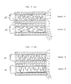
- Figs. 1 and 2 The double structure of the devices having a guest-host type liquid crystal display panel are shown in Figs. 1 and 2.
- the device of Fig. 1 has is for B/W display, and that of Fig. 2 has a color filter for full color display.
- Numerals in these figures indicate the following element:
- Panel A is the first display panel of light scattering type
- panel B is the second display panel of guest-host type containing a dichroic dye.
- Fig. 1-(a) in which no voltage is applied to panel A, light incident on the side of panel A is scattered in light controlling layer 5 to make white turbidity, while some light going straight enters into panel B to which a voltage is applied, is transmitted therethrough without being substantially absorbed by black dichroic dye 4, and reflected on white reflective plate 7 on the back side whereby the device gives a white vision when seen from the side of panel A.
- Fig. 1-(b) in which a voltage is applied to panel A, incident light is transmitted through light controlling layer 5 and enters into panel B to which no voltage is applied.
- panel B incident light is absorbed by black dichroic dye 4, whereby the device gives a black vision when seen from the side of panel A.
- black dichroic dye 4 In panel B, incident light is absorbed by black dichroic dye 4, whereby the device gives a black vision when seen from the side of panel A.
- black dichroic dye 4 In order to make the black color clearer, a polarizer may be provided between panels A and B or on the back side of panel B.
- Fig. 2-(a) in which no voltage is applied to panel A, incident light is scattered in light controlling layer 5 to make white turbidity, while some light going straight enters into panel B with no voltage applied thereto.
- panel B the incident light is absorbed by black dichroic dye 4 so that the color of RGB color filter 8 is not visible from the side of panel A.
- Fig. 2-(b) in which a voltage is applied to panel A, incident light is transmitted through light controlling layer 5 and enters into panel B with a voltage applied thereto.
- the incident light is transmitted through panel B and RGB color filter 8 without being substantially absorbed by black dichroic dye 4 so that the color of RGB filter 8 is visible from the side of panel A.
- a polarizer may be provided between panels A and B or on the back side of panel B.
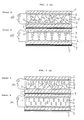
- the double structure of the liquid crystal device in which the second display panel is a twisted nematic liquid crystal display panel having a pair of polarizers is shown in Figs. 3 through 8.
- numeral 9 indicates a polarizer
- panel A is a light scattering type first liquid crystal display panel
- panel B is a twisted nematic type second liquid crystal display panel.
- the two polarizers 9 are perpendicular to each other.
- Fig. 3-(a) in which no voltage is applied to panel A, incident light is scattered in light controlling layer 5 to make white turbidity, while some light going straight enters into panel B with no voltage applied thereto.
- the incident light is transmitted through panel B while being polarized at an angle of 90 by twisted liquid crystal 3 and reflected by white reflective plate 7 on the back side, whereby the device looks white when seen from the side of panel A.
- Fig. 3-(b) in which a voltage is applied to panel A, incident light is transmitted through light controlling layer 5 and enters into panel B with a voltage applied thereto.
- the incident light is cut off by a pair of polarizers 9 perpendicular to each other, whereby the device gives a black vision when seen from the side of panel A.
- Fig. 3 While the device of Fig. 3 is of a reflection type, the same mechanism also applies to a device of transmission type in which reflective plate 7 is not provided and a back light is set instead at the back of panel B.
- panel A is a first liquid crystal display panel of a light scattering type
- panel B is a second liquid crystal display panel of twisted nematic type in which a pair of polarizers 9 are parallel to each other.
- Fig. 4-(a) in which no voltage is applied to panel A, and a voltage is applied to panel B, incident light is scattered in light controlling layer 5 of panel A to make white turbidity while some light going straight enters into panel B.
- the incident light is transmitted through panel B and reflected on white reflective plate 7, whereby the device looks white when seen from the side of panel A.
- Fig. 4-(b) in which a voltage is applied to panel A, and no voltage is applied to panel B, incident light is transmitted through light controlling layer 5 and enters into panel B, where it is polarized at an angle of 90 by twisted light crystal material 3 and cut off by a pair of parallel polarizers 9, whereby the device gives a black vision when seen from the side of panel A.
- a reflection type While the device of Fig. 4 is of a reflection type, the same mechanism also applies to a device of a transmission type in which reflective plate 7 is not provided and, instead, a back light is set on the back side of panel B.
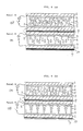
- Figs. 5 and 6 show the liquid crystal device of the present invention for color display, in which numeral 10 is a color polarizer.
- panel A is a first liquid crystal display panel of a light scattering type
- panel B is a second liquid crystal display panel of a twisted nematic type
- a pair of polarizers 9, 10 are perpendicular to each other.
- Fig. 5-(a) in which voltage is applied to neither panel A or panel B, incident light is scattered in light controlling layer 5 of panel A to make white turbidity, while some light going straight enters into panel B.
- the incident light on panel B is transmitted therethrough while being polarized at an angle of 90 by twisted liquid crystal material 3 and reflected on white reflective layer 7, whereby the device looks white when seen from the side of panel A.
- Fig. 5-(b) in which a voltage is applied to both panels A and B, incident light is transmitted through panel A and enters into panel B and cut off by a pair of polarizers 9, 10, whereby the device makes a color display when seen from the side of panel A.
- a reflection type the same mechanism also applies to a device of a transmission type in which reflective plate 7 is not provided and, instead, a back light is provided on the back side of panel B.
- panel A is a first liquid crystal display panel of light scattering type
- panel B is a second liquid crystal display panel of a twisted nematic type
- a pair of polarizers 9, 10 are parallel to each other.
- Fig. 6-(a) in which no voltage is applied to panel A, and a voltage is applied to panel B, incident light is scattered in light controlling layer 5 of panel A, while some light going straight enters into panel B.
- the incident light on panel B is transmitted therethrough and reflected on white reflective layer 7, whereby the device looks white when seen from the side of panel A.
- Fig. 6-(b) in which a voltage is applied to panel A, and no voltage is applied to panel B, incident light is transmitted through panel A and enters into panel B, where it is polarized at an angle of 90 by liquid crystal material 3 and cut off by a pair of parallel polarizers 9, 10, whereby the device makes a color display when seen from the side of panel A.
- a reflection type While the device of Fig. 6 is of a reflection type, the same mechanism also applies to a device of a transmission type in which reflective plate 7 is not provided and, instead, a back light is proved on the back side of panel B.
- Figs. 7 and 8 show the liquid crystal device of the present invention which has a color filter for full color display.
- panel A is a first liquid crystal display panel of a light scattering type
- panel B is a second liquid crystal display panel of a twisted nematic type
- a pair of polarizers 9 are parallel to each other.
- Fig. 7-(b) in which a voltage is applied to both panels A and B, incident light is transmitted through panel A and enters into panel B, where it is transmitted through RGB color filter 8 to make the color of RGB color filter 8 visible from the side of panel A.
- Fig. 7 While the device of Fig. 7 is of a reflection type, the same mechanism also applies to a device of a transmission type in which reflective plate 7 is not provided and, instead, a back light is proved on the back side of panel B.
- panel A is a first liquid crystal display panel of a light scattering type
- panel B is a second liquid crystal display panel of a twisted nematic type
- a pair of polarizers 9 are perpendicular to each other.
- Fig. 8-(b) in which a voltage is applied to panel A, and no voltage is applied to panel B, incident light is transmitted through panel A and enters into panel B, where it is transmitted therethrough while being polarized at an angle of 90 by twisted liquid crystal 3 and then transmitted through RGB color filter 8, whereby the color of RGB color filter 8 is visible from the side of panel A.
- Fig. 8 While the device of Fig. 8 is of a reflection type, the same mechanism also applies to a device of a transmission type in which reflective plate 7 is not provide and, instead, a back light is provided on the back of panel B.
- the light scattering liquid crystal devices shown in Figs. 1 through 8 are excellent in contrast. If desired, a display with excellent grey scale level can easily be obtained by merely changing the manner of combination of the two panels in each case with the driving circuit being unchanged.
- the twist angle is not limited to 90 and it is preferably in the range of 70 to 110°.
- the second display panel according to the present invention is not limited to a twisted nematic mode liquid crystal display panel and it may be a super-twisted nematic mode liquid crystal display panel, the twist angle of which is preferably in the range of 180 to 270°.
- the light scattering liquid crystal device having a double structure according to the present invention can be used with a conventionally known active device.
- the active device can be used either in the first or second display panel. It is preferred, however, to use the active device in the first display panel.
- various nematic liquid crystal display panels can be used as the second display panel, it is preferred to use a super-twisted nematic mode liquid crystal display panel which has a retardation film and a pair of polarizers.
- Substrates which can be used in the present invention include hard materials such as glass and flexible materials such as synthetic resin films.
- a pair of substrates are assembled to face to each other with an appropriate gap therebetween.
- the substrates should be transparent so that the entire or part of the supported liquid crystal layer and light controlling layer containing a transparent solid substance may be visible from the outside.
- a flexible material such as a synthetic resin film
- it can be used as fixed on a hard material.
- a spacer for gap retention may be incorporated between the two substrates as is usual in conventional liquid crystal devices.
- useful spacers are Mylar, alumina, rod type glass fiber, glass beads, polymer beads, etc.
- the liquid crystal material which can be used in the present invention includes not only a single liquid crystal compound but of course a mixture comprising two or more liquid crystal compounds and, if desired, other substances. All the materials recognized as liquid crystal materials in the art can be employed. Among them, those having a positive dielectric anisotropy are preferred.
- Liquid crystals to be used preferably include nematic liquid crystals, smectic liquid crystals, and cholesteric liquid crystals, with nematic liquid crystals being particularly preferred.
- the liquid crystals may contain chiral compounds, e.g., chiral dopants, cholesteric liquid crystals, chiral nematic liquid crystals, and chiral smectic liquid crystals.
- desired characteristics such as an isotropic liquid-liquid crystal phase transition temperature, a melting point, a viscosity, birefringence (An), dielectric anisotropy (LlE), and miscibility with a polymerizable composition.
- liquid crystal compounds are 4-substituted benzoic acid 4'-substituted phenyl esters, 4-substituted cyclohexanecarboxylic acid 4'-substituted phenyl esters, 4-substituted cyclohexanecarboxylic acid 4'-substituted biphenyl esters, 4-(4-substituted cyclohexanecarbonyloxy)benzoic acid 4'-substituted phenyl esters, 4-(4-substituted cyclohexyl)benzoic acid 4'-substituted phenyl esters, 4-(4-substituted cyclohexyl)benzoic acid 4'-substituted cyclohexyl esters, 4-substituted-4'-substituted biphenyls, 4-substituted phenyl-4'-substituted cyclohexy
- the light controlling layer of the first panel includes a dispersion of microcapsules of liquid crystals obtained by encapsulation with polyvinyl alcohol, etc. as disclosed in JP-W-58-501631, a dispersion of liquid crystal droplets in an epoxy resin matrix as disclosed in JP-W-61-502128, a dispersion of liquid crystal droplets in a photocured polymer which is obtained by phase separation by exposure to light as disclosed in JP-A-61-305528, and a continuous phase of a liquid crystal material in which a polymer forms a three-dimensional network as disclosed in JP-A-1-198725.
- a light controlling layer comprising a continuous phase of a liquid crystal material in which a polymer forms a three-dimensional network preferably contains at least 60% by weight, and particularly from 70 to 90% by weight, of the liquid crystal material.
- the transparent solid substance forming a network structure in the light controlling layer preferably includes thermosetting resins and ultraviolet curing resins obtained by polymerization of polymer-forming monomers or oligomers.
- polystyrene and derivatives thereof e.g., chlorostyrene, a-methylstyrene, and divinylbenzene
- acrylates, methacrylates or fumarates having a substituent e.g., methyl, ethyl, propyl, butyl, amyl, 2-ethylhexyl, octyl, nonyl, dodecyl, hexadecyl, octadecyl, cyclohexyl, benzyl, methoxyethyl, butoxyethyl, phenoxyethyl, allyl, methallyl, glycidyl, 2-hydroxyethyl, 2-hydroxypropyl, 3-chloro-2-hydroxypropyl, dimethylaminoethyl, and diethylaminoethyl; a mono- or poly-(meth)acrylate
- Preferred of them are trimethylolpropane triacrylate, tricyclodecanedimethylol diacrylate, polyethylene glycol diacrylate, polypropylene glycol diacrylate, hexanediol diacrylate, neopentyl glycol diacrylate, and tris(acryloxyethyl) isocyanurate.
- polymer-forming oligomers include caprolactone-modified hydroxypivalic ester neopentyl glycol diacrylate.
- Polymerization initiators to be used include 2-hydroxy-2-methyl-1-phenylpropan-1-one ("Darocure 1173” produced by Merck Co.), 1-hydroxycyclohexyl phenyl ketone ("Irgacure 184" produced by Ciba Geigy), 1-(4-isopropylphenyl)-2-hydroxy-2-methylpropan-1-one (“Darocure 1116” produced by Merck Co.), benzyl dimethyl ketal (“Irgacure 651” produced by Ciba Geigy), 2-methyl-1-[4-(methylthio)phenyl]-2-morpholinopropane-1 (“Irgacure 907" produced by Ciba Geigy), a mixture of 2,4-diethylthioxanthone ("Kayacure DETX” produced by Nippon Kayaku Co., Ltd.) and ethyl p-dimethylaminobenzoate ("Kayacure EPA
- the light controlling layer comprising a continuous layer of a liquid crystal material in which a transparent solid substance forms a uniform three-dimensional network structure
- a uniform solution comprising (a) a liquid crystal material, (b) a polymer-forming monomer or oligomer and, if desired, (c) a photopolymerization initiator while in an isotropic phase into a gap between a pair of substrates having a transparent electrode layer and applying radiation, e.g., ultraviolet rays and electron rays, or heat to the filled solution to cause polymerization curing to form a three-dimensional network structure.
- the solution may be supported between the substrates by coating the solution on one of substrates having a transparent electrode layer with an appropriate coater, e.g., a spin coater, and then superposing the other substrate thereon.
- Methods for uniformly forming a network layer of a transparent solid substance on a substrate are not limited to the above-mentioned techniques.
- the thickness of the light controlling layer may be controlled by incorporating a spacer into the solution to be filled or coated or by previously coating a spacer on the substrate.
- the thus formed three-dimensional network structure of a transparent solid substance preferably has an average mesh size ranging from 0.2 to 2 I .Lm. If the mesh size is too large or too small for a wavelength of light, light scattering properties tend to be reduced. In order to obtain a contrast sufficient for the end use between opaqueness due to light scattering and electrically induced transparency, the thickness of the light controlling layer preferably ranges from 2 to 30 am, and particularly from 5 to 20 am.
- liquid crystal materials which can be used in the second liquid crystal display panel are not particularly limited, and any of those usable in the first display panel can be adopted.
- Dichroic dyes which can be used in the guest-host type liquid crystal display panel are not particularly limited as far as suitable for liquid crystal use.
- suitable dichroic dyes include anthraquinone dyes, azo dyes, quinophthalone dyes, perylene dyes, coumarin dyes, thioindigo dyes, merocyanine dyes, styryl dyes, and oxonol dyes.
- dichroic dyes are commercially available under trade names of "SI-497” (blue hue), “M-137” (blue hue), “SI-426” (red hue), “S-416” (black hue), and “S-344" (black hue), all produced by Mitsui Toatsu Chemicals Inc.; "LCD-118” (blue hue), “LCD-208” (red hue), and “LCD-465" (black hue), all produced by Nippon Kayaku Co., Ltd.; and "CLD-506” (blue hue) produced by Sumitomo Chemical Co., Ltd.
- the dichroic dye is preferably added in an amount of from 0.01 to 10% by weight based on the liquid crystal material.
- the guest-host type liquid crystal display panel can be produced according to well-known methods.
- a double structure of the thus produced light scattering type liquid crystal display panel and guest-host type liquid crystal display panel provides a light scattering liquid crystal device of direct view type making a B/W or full color display with high contrast and brightness.
- the twisted or super-twisted nematic liquid crystal display panel which can be used as the second display panel is not particularly restricted, and any of known twisted nematic liquid crystal display elements for single use can be employed.
- the two polarizers which can be used in the twisted or super-twisted nematic liquid crystal display panel is selected appropriately from so-called normally white or normally black polarizers according to whether weight is attached to contrast or visual characteristics.
- the color polarizers or color filters can be selected without any particular restriction.
- Suitable commercially available polarizers include “LLC 2-81-12S” (neutral gray), “SCR-18” (red), “SCB-18” (blue), “SCG-18” (green), and “SCM-18” (magenta), all produced by Sanritsu Denki K.K.
- color filter 8 of panel B in Figs. 7 and 8 is provided between substrate 1 and transparent electrode layer 2 on the side farther from panel A, it may be provided between substrate 1 and polarizer 9 or between polarizer 9 and reflective player 7 on the same side according to the end use, for example large-sized display or precise display, or from the economical consideration.
- fixing of the light scattering panel A and the nematic panel B can be effected with an adhesive, a curing resin, etc. or by use of a polarizer having an adhesive layer on both sides thereof. Further, an air layer may be present between panels A and B.
- a solution consisting of 19.8% of trimethylolpropane triacrylate as a polymer-forming monomer, 0.2% of 2-hydroxy-2-methyl-1-phenylpropan-1-one as a polymerization initiator, and 80% of liquid crystal material (A) having the following composition was prepared, and a small amount of alumina powder having an average particle size of 10 ⁇ m was added thereto as a spacer.
- the mixture was filled between a pair of 20 cm wide and 20 cm long glass plates each having an ITO electrode layer, assembled with an electrode gap of 11 ⁇ m.
- the resulting unit panel was passed under a metal halide lamp (80 W/cm 2 ) at a speed of 3.5 m/min to irradiate ultraviolet light at a dose corresponding to 500 mJ/cm 2 on the liquid material to cure the polymer-forming monomer.
- the resulting panel was used as panel A.
- a general twisted nematic liquid crystal device comprising a pair of transparent substrates each having an electrode layer and a liquid crystal material comprising 98% of "RDX-5082" (a liquid crystal produced by Rodic Co.) and 2% of a black dichroic dye "S-416" was set on the above prepared panel A with panel A upside.
- the cross section of the resulting device is shown in Fig. 1.
- a contrast ratio of (a) the state with panel A “off” and panel B driven at 5V to (b) the state with panel A driven at 20 V and panel B "off” was 28:1.
- Panel A was produced in the same manner as in Example 1.
- a twisted nematic liquid crystal display panel comprising a pair of neutral gray polarizers "LLC 2-81-12S" perpendicular to each other having filled therebetween a liquid crystal material "RDX-5082” was prepared, and a reflective plate was attached to one of the polarizers to obtain panel B.
- Panels A and B were set up panel A upside and the reflective plate of panel B downside.
- the cross section of the resulting device is shown in Fig. 3.
- a contrast ratio of (a) the state with no voltage applied to either panel A or B (Figs. 3-(a)) to (b) the state with panel A driven at 20 V and panel B driven at 5 V (Fig. 3-(b)) was 32:1.
- Panel A was prepared in the same manner as in Example 1. A black back screen was placed on the back side of panel A to prepare a liquid crystal device. The contrast ratio of the device was 6:1.
- a liquid crystal device having a double structure was prepared in the same manner as in Example 2, except that the neutral gray polarizer with a reflective plate was replaced with a red color polarizer "SCR-18" with a reflective plate. The resulting device made a clear white/red display.
- a liquid crystal device having a double structure was prepared in the same manner as in Example 2, except for replacing the neutral gray polarizer with a reflective plate with a blue color polarizer "SCB-18", a green color polarizer “SCG-18”, or a magenta color polarizer “SCM-18" each with a reflective plate. Any of the resulting devices made a clear color display.
- a direct view type liquid crystal device having a double structure was prepared in the same manner as in Example 2, except for using a TFT (Thin Film Transistor)-twisted nematic liquid crystal panel having an RGB color filter as panel B.
- the resulting liquid crystal device made a clear full color display.
- the light scattering liquid crystal device of double structure achieves an extremely high contrast when formulated into a direct view type as compared with the conventional light scattering liquid crystal devices having a single panel structure.
- a combination of the first panel with a guest-host liquid crystal panel containing a dichroic dye and having a color filter or with a twisted nematic liquid crystal panel having a color filter makes it possible to accomplish a direct view type full color display that has been impossible with the conventional light scattering liquid crystal devices.
- liquid crystal device of the present invention is useful as a direct view type display, for example, as a computer terminal display.
Applications Claiming Priority (6)
| Application Number | Priority Date | Filing Date | Title |
|---|---|---|---|
| JP121102/91 | 1991-05-27 | ||
| JP12110291A JP3182695B2 (ja) | 1991-05-27 | 1991-05-27 | 光散乱形液晶2層パネル |
| JP16822491 | 1991-07-09 | ||
| JP168224/91 | 1991-07-09 | ||
| JP16315/92 | 1992-01-31 | ||
| JP1631592 | 1992-01-31 |
Publications (3)
| Publication Number | Publication Date |
|---|---|
| EP0516076A2 true EP0516076A2 (de) | 1992-12-02 |
| EP0516076A3 EP0516076A3 (en) | 1993-03-24 |
| EP0516076B1 EP0516076B1 (de) | 1999-04-07 |
Family
ID=27281357
Family Applications (1)
| Application Number | Title | Priority Date | Filing Date |
|---|---|---|---|
| EP92108936A Expired - Lifetime EP0516076B1 (de) | 1991-05-27 | 1992-05-27 | Flüssigkristallvorrichtung |
Country Status (4)
| Country | Link |
|---|---|
| US (1) | US5296952A (de) |
| EP (1) | EP0516076B1 (de) |
| DE (1) | DE69228843T2 (de) |
| HK (1) | HK1008697A1 (de) |
Cited By (7)
| Publication number | Priority date | Publication date | Assignee | Title |
|---|---|---|---|---|
| EP0939331A3 (de) * | 1998-02-27 | 2000-04-19 | Asulab S.A. | Anzeigeeinheit mit zwei aufeinander liegenden Anzeigevorrichtungen |
| US6515942B2 (en) | 1998-02-27 | 2003-02-04 | Asulab S.A. | Display assembly including two superposed display devices |
| WO2004049051A1 (en) * | 2002-11-22 | 2004-06-10 | Koninklijke Philips Electronics N.V. | Transflective liquid crystal display device |
| EP1852731A1 (de) * | 2006-05-05 | 2007-11-07 | Acer Incorporated | Doppelbildschirmanzeige, Flachbildschirm mit einer Doppelbildschirmanzeige und Verfahren zur Bildanzeige nach Abschalten des Flachbildschirms |
| CN106249492A (zh) * | 2016-10-12 | 2016-12-21 | 京东方科技集团股份有限公司 | 显示装置及其工作方法 |
| US10025150B2 (en) | 2013-02-04 | 2018-07-17 | Ortus Technology Co., Ltd. | Liquid crystal display |
| CN112925126A (zh) * | 2019-12-05 | 2021-06-08 | 咸阳彩虹光电科技有限公司 | 黑白显示面板、双层液晶显示基板及双层液晶显示面板 |
Families Citing this family (39)
| Publication number | Priority date | Publication date | Assignee | Title |
|---|---|---|---|---|
| JPH05303086A (ja) * | 1991-05-01 | 1993-11-16 | Canon Inc | 液晶素子および表示装置、それを用いた表示方法 |
| US5452113A (en) * | 1991-06-21 | 1995-09-19 | Nec Corporation | Color display element having PDLC layers and color filter |
| JPH05264972A (ja) * | 1992-03-18 | 1993-10-15 | Canon Inc | 表示素子および表示装置 |
| US5693421A (en) * | 1992-12-22 | 1997-12-02 | Dai Nippon Printing Co., Ltd. | Information recording medium and information recording and reproducing method |
| WO1994018598A1 (de) * | 1993-02-03 | 1994-08-18 | Horst Prehn | Verfahren und vorrichtung zur modulation von bildern für die darstellung optischer effekte |
| US6437846B1 (en) * | 1993-03-15 | 2002-08-20 | Seiko Epson Corporation | Liquid crystal display device and electronic device including same |
| US6229514B1 (en) | 1995-11-13 | 2001-05-08 | Array Printers Publ. Ab | Display device and method for visualizing computer generated image information |
| US5854614A (en) * | 1996-11-18 | 1998-12-29 | Array Printers Ab Publ. | Display device and method for visualizing computer generated image information |
| US5594573A (en) * | 1993-10-15 | 1997-01-14 | August; Gregg D. | Image display glasses having an LCD for displaying an image wherein the image provides for viewing by others |
| JP3068400B2 (ja) * | 1994-03-17 | 2000-07-24 | シャープ株式会社 | 液晶表示装置の製造方法 |
| US5641426A (en) * | 1994-04-29 | 1997-06-24 | Minnesota Mining And Manufacturing Company | Light modulating device having a vinyl ether-based matrix |
| JPH09512580A (ja) * | 1994-04-29 | 1997-12-16 | ミネソタ マイニング アンド マニュファクチャリング カンパニー | 酸性反応体から製造されたマトリックスを有する光変調素子 |
| GB2299698A (en) | 1995-03-30 | 1996-10-09 | Sharp Kk | Colour display |
| US5831700A (en) * | 1995-05-19 | 1998-11-03 | Kent State University | Polymer stabilized four domain twisted nematic liquid crystal display |
| US5989451A (en) * | 1997-02-07 | 1999-11-23 | Queen's University At Kingston | Compounds and methods for doping liquid crystal hosts |
| US6278430B1 (en) | 1998-03-06 | 2001-08-21 | Array Printers Ab | Thermosensitive display device |
| CN100430787C (zh) * | 2005-07-21 | 2008-11-05 | 宏碁股份有限公司 | 双层显示面板及其平面显示器与其关机后图像显示方法 |
| US20070258023A1 (en) * | 2006-05-08 | 2007-11-08 | Acer Incorporated | Dual-panel display panel, flat-panel display employing a dual-panel display panel, and method of showing images after the flat-panel display is turned off |
| CA2564461A1 (en) * | 2006-10-17 | 2008-04-17 | Ibm Canada Limited - Ibm Canada Limitee | Double-sided lcd panel |
| US7643107B2 (en) * | 2007-05-01 | 2010-01-05 | Citizen Holdings Co., Ltd. | Liquid crystal display apparatus |
| CN101329450B (zh) * | 2008-07-24 | 2010-06-02 | 深圳超多维光电子有限公司 | 2d/3d可切换显示设备 |
| US8330882B2 (en) * | 2009-02-25 | 2012-12-11 | Industrial Technology Research Institute | Image display capable of being an electronic curtain |
| TWM410950U (en) * | 2011-03-16 | 2011-09-01 | Lbc Technology Co Ltd | Exhibition machine having brightness contrast effect |
| JP5857599B2 (ja) * | 2011-09-30 | 2016-02-10 | セイコーエプソン株式会社 | スクリーンおよび画像表示システム |
| JP5866936B2 (ja) | 2011-09-30 | 2016-02-24 | セイコーエプソン株式会社 | 画像表示システム |
| US8976306B2 (en) * | 2013-01-09 | 2015-03-10 | Shenzhen China Star Optoelectronics Technology Co., Ltd. | Shutter glasses and related 3D display system |
| CN103676364A (zh) * | 2013-12-20 | 2014-03-26 | 深圳市华星光电技术有限公司 | 显示面板 |
| KR101732789B1 (ko) * | 2014-04-04 | 2017-05-08 | 주식회사 엘지화학 | 액정 소자 |
| KR102314707B1 (ko) * | 2014-06-27 | 2021-10-20 | 엘지디스플레이 주식회사 | 광 제어 장치, 상기 광 제어 장치의 제조방법, 및 상기 광 제어 장치를 포함한 투명표시장치 |
| US9989798B2 (en) | 2014-06-27 | 2018-06-05 | Lg Display Co., Ltd. | Light controlling apparatus, method of fabricating the light controlling apparatus and transparent display device including the light controlling apparatus with transparent mode and light shielding mode |
| US20170138120A1 (en) * | 2014-07-11 | 2017-05-18 | Panasonic Intellectual Property Management Co., Ltd. | Optical switching device and building material |
| WO2016006180A1 (ja) * | 2014-07-11 | 2016-01-14 | パナソニックIpマネジメント株式会社 | 光スイッチングデバイス及びその製造方法、並びに建材 |
| KR102521487B1 (ko) * | 2015-09-15 | 2023-04-14 | 삼성전자주식회사 | 스마트 윈도우 시스템 및 그 제어 방법 |
| KR20170044373A (ko) * | 2015-10-15 | 2017-04-25 | 엘지전자 주식회사 | 디스플레이 장치 |
| JP6897002B2 (ja) * | 2016-04-11 | 2021-06-30 | 凸版印刷株式会社 | 表示装置 |
| CN106483694B (zh) * | 2017-01-03 | 2019-09-27 | 京东方科技集团股份有限公司 | 显示屏、显示装置及显示方法 |
| TWI632416B (zh) * | 2017-10-06 | 2018-08-11 | 友達光電股份有限公司 | 顯示面板 |
| KR102380640B1 (ko) * | 2017-11-23 | 2022-03-29 | 엘지디스플레이 주식회사 | 액정캡슐을 포함하는 액정표시장치 |
| CN112558358A (zh) | 2019-09-26 | 2021-03-26 | 默克专利股份有限公司 | 双层液晶设备和制造方法 |
Citations (5)
| Publication number | Priority date | Publication date | Assignee | Title |
|---|---|---|---|---|
| JPS5588022A (en) * | 1978-12-26 | 1980-07-03 | Seiko Epson Corp | Liquid crystal display panel |
| JPS5918925A (ja) * | 1982-07-23 | 1984-01-31 | Asahi Glass Co Ltd | 液晶表示素子 |
| EP0313053A2 (de) * | 1987-10-20 | 1989-04-26 | Dainippon Ink And Chemicals, Inc. | Flüssigkristallvorrichtung |
| EP0326248A2 (de) * | 1988-01-25 | 1989-08-02 | Raychem Corporation | Anzeigevorrichtung |
| JPH03102326A (ja) * | 1989-09-18 | 1991-04-26 | Seikosha Co Ltd | 多色表示装置 |
Family Cites Families (14)
| Publication number | Priority date | Publication date | Assignee | Title |
|---|---|---|---|---|
| CH564206A5 (de) * | 1973-09-27 | 1975-07-15 | Bbc Brown Boveri & Cie | |
| US3967881A (en) * | 1974-04-04 | 1976-07-06 | Matsushita Electric Industrial Co., Ltd. | Liquid crystal display |
| JPS525550A (en) * | 1975-07-02 | 1977-01-17 | Matsushita Electric Ind Co Ltd | Device for indicating liquid crystals |
| JPS5438150A (en) * | 1977-09-01 | 1979-03-22 | Seiko Instr & Electronics Ltd | Color liquid crystal display device |
| US4435047A (en) * | 1981-09-16 | 1984-03-06 | Manchester R & D Partnership | Encapsulated liquid crystal and method |
| US4707080A (en) * | 1981-09-16 | 1987-11-17 | Manchester R & D Partnership | Encapsulated liquid crystal material, apparatus and method |
| EP0180592B1 (de) * | 1984-03-19 | 1995-08-02 | Kent State University | Lichtmodulierendes Material, das in einer Kunstharzmatrix dispergierte Flüssigkristalle umfasst |
| US4688901A (en) * | 1984-06-11 | 1987-08-25 | Johnson Light Valve Inc. | Liquid crystal light valve method and apparatus using right and left-handed twist cholesteric liquid crystal |
| JPS61100725A (ja) * | 1984-10-24 | 1986-05-19 | Stanley Electric Co Ltd | 液晶表示装置 |
| DE3752026T2 (de) * | 1986-12-23 | 1997-06-26 | Asahi Glass Co Ltd | Optische Flüssigkristall-Vorrichtung und Verfahren zu ihrer Herstellung. |
| JPH01200232A (ja) * | 1988-02-04 | 1989-08-11 | Sharp Corp | 強誘電性液晶表示装置 |
| US4886343A (en) * | 1988-06-20 | 1989-12-12 | Honeywell Inc. | Apparatus and method for additive/subtractive pixel arrangement in color mosaic displays |
| JP2675158B2 (ja) * | 1988-12-07 | 1997-11-12 | シャープ株式会社 | 液晶表示装置 |
| JPH04199024A (ja) * | 1990-11-29 | 1992-07-20 | Hitachi Ltd | 液晶表示素子およびそれを用いた表示装置 |
-
1992
- 1992-05-27 DE DE69228843T patent/DE69228843T2/de not_active Expired - Fee Related
- 1992-05-27 EP EP92108936A patent/EP0516076B1/de not_active Expired - Lifetime
-
1993
- 1993-08-02 US US08/100,207 patent/US5296952A/en not_active Expired - Lifetime
-
1998
- 1998-07-28 HK HK98109468A patent/HK1008697A1/xx not_active IP Right Cessation
Patent Citations (5)
| Publication number | Priority date | Publication date | Assignee | Title |
|---|---|---|---|---|
| JPS5588022A (en) * | 1978-12-26 | 1980-07-03 | Seiko Epson Corp | Liquid crystal display panel |
| JPS5918925A (ja) * | 1982-07-23 | 1984-01-31 | Asahi Glass Co Ltd | 液晶表示素子 |
| EP0313053A2 (de) * | 1987-10-20 | 1989-04-26 | Dainippon Ink And Chemicals, Inc. | Flüssigkristallvorrichtung |
| EP0326248A2 (de) * | 1988-01-25 | 1989-08-02 | Raychem Corporation | Anzeigevorrichtung |
| JPH03102326A (ja) * | 1989-09-18 | 1991-04-26 | Seikosha Co Ltd | 多色表示装置 |
Non-Patent Citations (3)
| Title |
|---|
| PATENT ABSTRACTS OF JAPAN vol. 15, no. 296 (P-1231)26 July 1991 & JP-A-03 102 326 ( SEIKOSHA ) 26 April 1991 * |
| PATENT ABSTRACTS OF JAPAN vol. 4, no. 138 (P-29)17 September 1980 & JP-A-55 088 022 ( SEIKO ) 3 March 1980 * |
| PATENT ABSTRACTS OF JAPAN vol. 8, no. 109 (P-275)22 May 1984 & JP-A-59 018 925 ( ASAHI ) 31 January 1984 * |
Cited By (9)
| Publication number | Priority date | Publication date | Assignee | Title |
|---|---|---|---|---|
| EP0939331A3 (de) * | 1998-02-27 | 2000-04-19 | Asulab S.A. | Anzeigeeinheit mit zwei aufeinander liegenden Anzeigevorrichtungen |
| US6515942B2 (en) | 1998-02-27 | 2003-02-04 | Asulab S.A. | Display assembly including two superposed display devices |
| WO2004049051A1 (en) * | 2002-11-22 | 2004-06-10 | Koninklijke Philips Electronics N.V. | Transflective liquid crystal display device |
| US7423664B2 (en) | 2002-11-22 | 2008-09-09 | Tpo Hong Kong Holding Limited | Transflective liquid crystal display device having alignment film covering plural isolated stacks of resin and diffusive reflective plate layers |
| EP1852731A1 (de) * | 2006-05-05 | 2007-11-07 | Acer Incorporated | Doppelbildschirmanzeige, Flachbildschirm mit einer Doppelbildschirmanzeige und Verfahren zur Bildanzeige nach Abschalten des Flachbildschirms |
| US10025150B2 (en) | 2013-02-04 | 2018-07-17 | Ortus Technology Co., Ltd. | Liquid crystal display |
| EP2952955B1 (de) * | 2013-02-04 | 2022-02-23 | Toppan Printing Co., Ltd. | Flüssigkristallanzeige |
| CN106249492A (zh) * | 2016-10-12 | 2016-12-21 | 京东方科技集团股份有限公司 | 显示装置及其工作方法 |
| CN112925126A (zh) * | 2019-12-05 | 2021-06-08 | 咸阳彩虹光电科技有限公司 | 黑白显示面板、双层液晶显示基板及双层液晶显示面板 |
Also Published As
| Publication number | Publication date |
|---|---|
| HK1008697A1 (en) | 1999-05-14 |
| EP0516076B1 (de) | 1999-04-07 |
| DE69228843D1 (de) | 1999-05-12 |
| US5296952A (en) | 1994-03-22 |
| DE69228843T2 (de) | 1999-08-26 |
| EP0516076A3 (en) | 1993-03-24 |
Similar Documents
| Publication | Publication Date | Title |
|---|---|---|
| EP0516076B1 (de) | Flüssigkristallvorrichtung | |
| US5327271A (en) | Liquid crystal device employing polymer network on one substrate and alignment layer or polymer network on other substrate | |
| EP0313053B1 (de) | Flüssigkristallvorrichtung | |
| US5304323A (en) | Liquid crystal devices and process for producing the same | |
| US5519519A (en) | Production method for a polymer dispersed liquid crystal display | |
| JP3131954B2 (ja) | 液晶デバイス | |
| EP0751202B1 (de) | Optisches Flüssigkristallelement, Flüssigkristallanzeigeelement und Flüssigkristall-Projektionanzeigegerät, dass dieses Element verwendet | |
| JP3864429B2 (ja) | 液晶デバイス | |
| JPH08160386A (ja) | 液晶表示装置 | |
| JPH05273576A (ja) | 光散乱形液晶2層パネル | |
| JPH08190086A (ja) | 液晶表示素子及びこれを用いた表示装置 | |
| JP3401681B2 (ja) | 液晶デバイス | |
| JP3401680B2 (ja) | 液晶デバイス | |
| JP3182695B2 (ja) | 光散乱形液晶2層パネル | |
| JP3680332B2 (ja) | 液晶表示素子及びこれを用いた表示装置 | |
| JP3552328B2 (ja) | 液晶デバイスの製造方法 | |
| JP3214118B2 (ja) | 液晶デバイスの製造方法 | |
| JP3485128B2 (ja) | 液晶デバイス及びこれを用いた液晶表示装置 | |
| JPH05281526A (ja) | 液晶表示素子 | |
| JP3195942B2 (ja) | 液晶デバイス | |
| JP3383921B2 (ja) | 液晶デバイス | |
| JP3010778B2 (ja) | 液晶デバイスの製造方法 | |
| JP3077402B2 (ja) | 液晶デバイスの製造方法 | |
| JPH11349949A (ja) | 高分子分散型液晶素子およびその製造方法 | |
| JPH055869A (ja) | 液晶デバイス |
Legal Events
| Date | Code | Title | Description |
|---|---|---|---|
| PUAI | Public reference made under article 153(3) epc to a published international application that has entered the european phase |
Free format text: ORIGINAL CODE: 0009012 |
|
| AK | Designated contracting states |
Kind code of ref document: A2 Designated state(s): DE FR GB |
|
| PUAL | Search report despatched |
Free format text: ORIGINAL CODE: 0009013 |
|
| AK | Designated contracting states |
Kind code of ref document: A3 Designated state(s): DE FR GB |
|
| 17P | Request for examination filed |
Effective date: 19930623 |
|
| 17Q | First examination report despatched |
Effective date: 19950328 |
|
| GRAG | Despatch of communication of intention to grant |
Free format text: ORIGINAL CODE: EPIDOS AGRA |
|
| GRAG | Despatch of communication of intention to grant |
Free format text: ORIGINAL CODE: EPIDOS AGRA |
|
| GRAH | Despatch of communication of intention to grant a patent |
Free format text: ORIGINAL CODE: EPIDOS IGRA |
|
| GRAH | Despatch of communication of intention to grant a patent |
Free format text: ORIGINAL CODE: EPIDOS IGRA |
|
| GRAA | (expected) grant |
Free format text: ORIGINAL CODE: 0009210 |
|
| AK | Designated contracting states |
Kind code of ref document: B1 Designated state(s): DE FR GB |
|
| REF | Corresponds to: |
Ref document number: 69228843 Country of ref document: DE Date of ref document: 19990512 |
|
| ET | Fr: translation filed | ||
| PLBE | No opposition filed within time limit |
Free format text: ORIGINAL CODE: 0009261 |
|
| STAA | Information on the status of an ep patent application or granted ep patent |
Free format text: STATUS: NO OPPOSITION FILED WITHIN TIME LIMIT |
|
| 26N | No opposition filed | ||
| REG | Reference to a national code |
Ref country code: GB Ref legal event code: IF02 |
|
| PGFP | Annual fee paid to national office [announced via postgrant information from national office to epo] |
Ref country code: DE Payment date: 20060522 Year of fee payment: 15 |
|
| PGFP | Annual fee paid to national office [announced via postgrant information from national office to epo] |
Ref country code: FR Payment date: 20060523 Year of fee payment: 15 |
|
| PGFP | Annual fee paid to national office [announced via postgrant information from national office to epo] |
Ref country code: GB Payment date: 20060525 Year of fee payment: 15 |
|
| GBPC | Gb: european patent ceased through non-payment of renewal fee |
Effective date: 20070527 |
|
| REG | Reference to a national code |
Ref country code: FR Ref legal event code: ST Effective date: 20080131 |
|
| PG25 | Lapsed in a contracting state [announced via postgrant information from national office to epo] |
Ref country code: DE Free format text: LAPSE BECAUSE OF NON-PAYMENT OF DUE FEES Effective date: 20071201 |
|
| PG25 | Lapsed in a contracting state [announced via postgrant information from national office to epo] |
Ref country code: GB Free format text: LAPSE BECAUSE OF NON-PAYMENT OF DUE FEES Effective date: 20070527 |
|
| PG25 | Lapsed in a contracting state [announced via postgrant information from national office to epo] |
Ref country code: FR Free format text: LAPSE BECAUSE OF NON-PAYMENT OF DUE FEES Effective date: 20070531 |