EP0514046B1 - Système et méthode de contrÔle et d'exécution de la gravure d'une plaquette - Google Patents
Système et méthode de contrÔle et d'exécution de la gravure d'une plaquette Download PDFInfo
- Publication number
- EP0514046B1 EP0514046B1 EP92303938A EP92303938A EP0514046B1 EP 0514046 B1 EP0514046 B1 EP 0514046B1 EP 92303938 A EP92303938 A EP 92303938A EP 92303938 A EP92303938 A EP 92303938A EP 0514046 B1 EP0514046 B1 EP 0514046B1
- Authority
- EP
- European Patent Office
- Prior art keywords
- profile data
- wafer
- thin film
- thickness profile
- dwell time
- Prior art date
- Legal status (The legal status is an assumption and is not a legal conclusion. Google has not performed a legal analysis and makes no representation as to the accuracy of the status listed.)
- Expired - Lifetime
Links
Images

Classifications
-
- H—ELECTRICITY
- H01—ELECTRIC ELEMENTS
- H01L—SEMICONDUCTOR DEVICES NOT COVERED BY CLASS H10
- H01L21/00—Processes or apparatus adapted for the manufacture or treatment of semiconductor or solid state devices or of parts thereof
- H01L21/02—Manufacture or treatment of semiconductor devices or of parts thereof
- H01L21/04—Manufacture or treatment of semiconductor devices or of parts thereof the devices having at least one potential-jump barrier or surface barrier, e.g. PN junction, depletion layer or carrier concentration layer
- H01L21/18—Manufacture or treatment of semiconductor devices or of parts thereof the devices having at least one potential-jump barrier or surface barrier, e.g. PN junction, depletion layer or carrier concentration layer the devices having semiconductor bodies comprising elements of Group IV of the Periodic System or AIIIBV compounds with or without impurities, e.g. doping materials
- H01L21/30—Treatment of semiconductor bodies using processes or apparatus not provided for in groups H01L21/20 - H01L21/26
- H01L21/302—Treatment of semiconductor bodies using processes or apparatus not provided for in groups H01L21/20 - H01L21/26 to change their surface-physical characteristics or shape, e.g. etching, polishing, cutting
-
- H—ELECTRICITY
- H01—ELECTRIC ELEMENTS
- H01L—SEMICONDUCTOR DEVICES NOT COVERED BY CLASS H10
- H01L21/00—Processes or apparatus adapted for the manufacture or treatment of semiconductor or solid state devices or of parts thereof
- H01L21/67—Apparatus specially adapted for handling semiconductor or electric solid state devices during manufacture or treatment thereof; Apparatus specially adapted for handling wafers during manufacture or treatment of semiconductor or electric solid state devices or components ; Apparatus not specifically provided for elsewhere
- H01L21/67005—Apparatus not specifically provided for elsewhere
- H01L21/67242—Apparatus for monitoring, sorting or marking
- H01L21/67253—Process monitoring, e.g. flow or thickness monitoring
-
- H—ELECTRICITY
- H01—ELECTRIC ELEMENTS
- H01J—ELECTRIC DISCHARGE TUBES OR DISCHARGE LAMPS
- H01J37/00—Discharge tubes with provision for introducing objects or material to be exposed to the discharge, e.g. for the purpose of examination or processing thereof
- H01J37/32—Gas-filled discharge tubes
- H01J37/32917—Plasma diagnostics
- H01J37/32935—Monitoring and controlling tubes by information coming from the object and/or discharge
- H01J37/32963—End-point detection
-
- H—ELECTRICITY
- H01—ELECTRIC ELEMENTS
- H01L—SEMICONDUCTOR DEVICES NOT COVERED BY CLASS H10
- H01L21/00—Processes or apparatus adapted for the manufacture or treatment of semiconductor or solid state devices or of parts thereof
- H01L21/02—Manufacture or treatment of semiconductor devices or of parts thereof
- H01L21/04—Manufacture or treatment of semiconductor devices or of parts thereof the devices having at least one potential-jump barrier or surface barrier, e.g. PN junction, depletion layer or carrier concentration layer
- H01L21/18—Manufacture or treatment of semiconductor devices or of parts thereof the devices having at least one potential-jump barrier or surface barrier, e.g. PN junction, depletion layer or carrier concentration layer the devices having semiconductor bodies comprising elements of Group IV of the Periodic System or AIIIBV compounds with or without impurities, e.g. doping materials
- H01L21/30—Treatment of semiconductor bodies using processes or apparatus not provided for in groups H01L21/20 - H01L21/26
- H01L21/302—Treatment of semiconductor bodies using processes or apparatus not provided for in groups H01L21/20 - H01L21/26 to change their surface-physical characteristics or shape, e.g. etching, polishing, cutting
- H01L21/306—Chemical or electrical treatment, e.g. electrolytic etching
- H01L21/3065—Plasma etching; Reactive-ion etching
-
- H—ELECTRICITY
- H01—ELECTRIC ELEMENTS
- H01L—SEMICONDUCTOR DEVICES NOT COVERED BY CLASS H10
- H01L21/00—Processes or apparatus adapted for the manufacture or treatment of semiconductor or solid state devices or of parts thereof
- H01L21/67—Apparatus specially adapted for handling semiconductor or electric solid state devices during manufacture or treatment thereof; Apparatus specially adapted for handling wafers during manufacture or treatment of semiconductor or electric solid state devices or components ; Apparatus not specifically provided for elsewhere
- H01L21/67005—Apparatus not specifically provided for elsewhere
- H01L21/67011—Apparatus for manufacture or treatment
- H01L21/67017—Apparatus for fluid treatment
- H01L21/67063—Apparatus for fluid treatment for etching
- H01L21/67069—Apparatus for fluid treatment for etching for drying etching
-
- H—ELECTRICITY
- H01—ELECTRIC ELEMENTS
- H01L—SEMICONDUCTOR DEVICES NOT COVERED BY CLASS H10
- H01L21/00—Processes or apparatus adapted for the manufacture or treatment of semiconductor or solid state devices or of parts thereof
- H01L21/70—Manufacture or treatment of devices consisting of a plurality of solid state components formed in or on a common substrate or of parts thereof; Manufacture of integrated circuit devices or of parts thereof
- H01L21/71—Manufacture of specific parts of devices defined in group H01L21/70
- H01L21/76—Making of isolation regions between components
- H01L21/762—Dielectric regions, e.g. EPIC dielectric isolation, LOCOS; Trench refilling techniques, SOI technology, use of channel stoppers
- H01L21/7624—Dielectric regions, e.g. EPIC dielectric isolation, LOCOS; Trench refilling techniques, SOI technology, use of channel stoppers using semiconductor on insulator [SOI] technology
- H01L21/76251—Dielectric regions, e.g. EPIC dielectric isolation, LOCOS; Trench refilling techniques, SOI technology, use of channel stoppers using semiconductor on insulator [SOI] technology using bonding techniques
-
- H—ELECTRICITY
- H01—ELECTRIC ELEMENTS
- H01L—SEMICONDUCTOR DEVICES NOT COVERED BY CLASS H10
- H01L22/00—Testing or measuring during manufacture or treatment; Reliability measurements, i.e. testing of parts without further processing to modify the parts as such; Structural arrangements therefor
- H01L22/10—Measuring as part of the manufacturing process
- H01L22/12—Measuring as part of the manufacturing process for structural parameters, e.g. thickness, line width, refractive index, temperature, warp, bond strength, defects, optical inspection, electrical measurement of structural dimensions, metallurgic measurement of diffusions
-
- H—ELECTRICITY
- H01—ELECTRIC ELEMENTS
- H01L—SEMICONDUCTOR DEVICES NOT COVERED BY CLASS H10
- H01L22/00—Testing or measuring during manufacture or treatment; Reliability measurements, i.e. testing of parts without further processing to modify the parts as such; Structural arrangements therefor
- H01L22/20—Sequence of activities consisting of a plurality of measurements, corrections, marking or sorting steps
-
- H—ELECTRICITY
- H01—ELECTRIC ELEMENTS
- H01J—ELECTRIC DISCHARGE TUBES OR DISCHARGE LAMPS
- H01J2237/00—Discharge tubes exposing object to beam, e.g. for analysis treatment, etching, imaging
- H01J2237/32—Processing objects by plasma generation
- H01J2237/33—Processing objects by plasma generation characterised by the type of processing
- H01J2237/334—Etching
Definitions
- the present invention generally relates to a system and a method for removing material from a wafer and, in particular, relates to one such system and method including means for removing material from a wafer in accordance with a predetermined profile.
- semiconductor devices are most frequently fabricated in a layer of high resistivity semiconductor material, usually silicon, by such methods as diffusion, epitaxial layer growth, ion implantation or perhaps a combination of these techniques.
- charge leakage paths also limit the circuits that can be achieved in both device density and bit storage lifetimes.
- the proximity of the bulk silicon wafer to the active device layer results in a reduced radiation hardness. That is, for a memory device, exposure to high radiation can result in "bit errors". Whereas the thin active device layer is substantially transparent to incident radiation the much thicker underlying wafer absorbs a substantial amount of such radiation. This high absorption results in free electrical carriers that migrate to the active device layer and create logic and/or memory errors.
- SOI silicon-on-insulator
- zone-melt recrystallization a polycrystalline silicon film is deposited on a thermally oxidized silicon wafer surface, the film and wafer are then locally heated to reduce recrystallization of the silicon film.
- the resulting film is not a single crystal but, rather, consists of a large number of grains. Due to the large lattice mismatch between the silicon and the insulator the resulting film has substantially higher defect densities and rougher surfaces than typical high quality bulk silicon and thus exhibit poorer electrical properties.
- SIMOX separation by implanted oxygen
- SOI wafers have been formed by using two standard silicon wafers.
- One standard wafer is, typically, thermally oxidized to provide a silicon dioxide layer of about one micrometer on both surfaces thereof.
- the oxidized wafer is then bonded to a polished surface of the other standard silicon wafer.
- the bonded assembly is thereafter thinned by a series of mechanical grinding and chemo-mechanical polishing steps applied to its unbonded surface.
- the thinning process currently involves, in essence, standard mechanical grinding and polishing steps wherein material is removed from the wafer simultaneously for all surface points, i.e., full wafer abrasive removal with a polishing tool at least as large as the wafer itself.
- the process utilizes the interface between the back surface of the base wafer and the grinding/polishing lap as a reference for achieving a flat upper surface of the wafer into which devices will be formed. This process, thus, assumes that both the base wafer back surface and the lap are initially very flat and that there is not particulate contamination therebetween.
- EP-A-0 488 642 which was cited under Article 54 (3) and (4) EPC with regard to its designated States of Germany, France and the United Kingdom, discloses a system for removing material from a wafer.
- US-A-4 758 304 discloses a method and apparatus using ion etching and ion assisted deposition to reform a surface of an object, such as a large lens, from its existing topography to a predetermined topography.
- the method comprises comparing the existing topography of the surface of the object to the predetermined topography. In one embodiment, the comparison can be used to distinguish objects having surfaces which are readily or economically reformable to the predetermined topography from those which are not suitable for such reforming.
- the method novelly utilizes an algorithm comprising image restoration.
- the ion etching structure of the apparatus comprises an ion source grid which can be used to provide an ion beam of a preselected spatial distribution.
- the grid is constructed of a nonconducting, vacuum compatible material, such as a ceramic sheet coated with a conductive layer on each side. Apertures are drilled through the grid in a selected pattern.
- the ion beam produced from a plasma source when a suitable voltage is applied across the coatings has a spatial distribution in accordance with the aperture pattern.
- the coatings comprise discrete corresponding areas on each surface and different voltages are applicable to each area to further control beam spatial distribution. Ion assisted deposition may be simultaneously performed under the algorithm to add material to the surface in accordance with the desired predetermined topography.
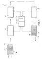
- a system, generally indicated at 10 in FIGURE 1, for removing material from a semiconductor wafer includes means 12 for determining thickness profile data for a surface of a wafer 14, means 16 for converting the thickness profile data to a dwell time versus position map 18 stored in a system controller 20 and means 22 for removing material from a surface 24 of the wafer 14 in accordance with the map 18 such that the wafer 14 has a preselected thickness profile.
- wafer as used herein is formed of a substrate and an insulating layer covered by a thin film.
- the system 10 can also include means 26 for delivering one or more wafers 14 to the thickness profile data determining means 12, means 28 for determining thickness profile data of a wafer 14 subsequent to removing material therefrom, and means 30 for transporting one or more wafers 14 from the means 22 for removing material.
- a typical wafer 14 shown in cross-section in FIGURES 2 includes a silicon support substrate 32 having a silicon film 34 affixed thereto and spaced apart therefrom by a layer 36 of insulating material, such as, for example, silicon dioxide, silicon nitride, or the like. Bonded silicon wafers are available from a number of semiconductor wafer manufacturers.
- the surfaces, 38 and 40, of the support substrate 32, the surfaces, 42 and 44, of the insulator 36 and the lower surface 46 of the silicon film 34 are irregular, i.e., not flat.
- the upper surface 24 of the silicon film 34 is shown in Figure 2A as it may appear before the application of conventional chemo-mechanical polishing techniques. Nevertheless, for the purposes of the present invention such gross conventional techniques may be used to initially remove material from the silicon film 34 to a minimum, but nonuniform, thickness on the order of about 5 micrometers.
- the silicon film 34 is, initially, a silicon wafer having an average thickness of about 200 micrometers.
- the peak-to-valley distances are usually on the order of about 10 micrometers but can also be on the order of 50 micrometers.
- conventional chemo-mechanical polishing techniques can be used to reduce the minimum thickness of the silicon film 34 to between about 3 micrometers and 5 micrometers without causing any single point of the film to be too thin to be useful.
- the typical wafer 14 is then conveyed to the means 12 for determining thickness profile data of the silicon film 34.
- the means 12 is an interferometer that computes thickness at each point of the surface on a point-by-point basis from the white light interference patterns.
- the thickness profile data determining means 12 can alternatively be, for example, an ellipsometer, a high frequency acoustic wave device, or a full surface interferometer. Each has advantages and disadvantages as well as preferential applicability.
- One of the primary criteria for selecting the thickness profile data determining means 12 is that the operating wavelength thereof must be within the transparency range of the material of the film or wafer.
- white light interferometry has advantage because many points can be rapidly measured to map the thickness profile data.
- laser transmission is advantageous because a free standing silicon film can be measured.
- the thickness profile of the silicon film 34 is determined across the entire upper surface 48 thereof. This can be accomplished by translating the thickness profile measuring instrument and the wafer 14 with respect to each other. For example, an interferometric beam can be raster scanned across the wafer 14, or alternatively, the wafer 14, can be moved with respect to a stationary interferometric instrument.
- the initial profile data representing the point-by-point thickness of the silicon film 34 is then processed by the converting means 16 to yield a dwell time versus position map 18 for the entire upper surface 48 of the silicon film 34.
- the preferred means 22 for material removal is a plasma etching puck having an etching footprint smaller than the thickness of material to be removed from the silicon film 34.
- the input data to the converting means 16 includes at least three factors, the measured initial thickness profile data, the desired final film thickness profile data and the spatial material removal rate pattern of the plasma etching puck. In the event that the spatial material removal rate pattern is unknown for a particular film material, empirical measurements should be taken on that material prior to the formation of the dwell time versus position map.
- the measured initial film thickness profile data and the desired target film thickness profile provide a thickness error map of material thickness to be removed from the silicon film 34. Effectively, in one instance, the thickness error map is generated by a point-by-point subtraction of the desired end thickness from the measured initial thickness. In the specific application where a final uniform film thickness is desired the material thickness error map would be the initial film thickness profile less a constant. It will be recognized that, any arbitrary film thickness profile can be produced by specifying a material thickness error map constructed from the initial measured film thickness profile data and the target film profile data.
- the converting means 16 can be the equivalent of the arithmetic logic unit of a personal computer including appropriate input, output, memory and other peripheral units.
- the system controller 20 can be any of the typical computer controllers readily available for machine control operations.
- the dwell time versus position map 18 is then computed from the thickness error map.
- the dwell time map represents the length of time that the plasma removal puck must spend at each specified position over the film surface 34 to produce the specified target film thickness profile.
- the dwell time map computation incorporates the spatial material removal rate of the plasma etching puck.
- the dwell map is calculated using a known two-dimensional fast Fourier transfer implementation of the Fourier Deconvolution Theorem on the film thickness error map.
- the dwell time map is used by the system controller 20 to generate a set of instructions to the translation mechanism of the apparatus.
- the instructions are used to control the velocity of the plasma puck over the silicon film 34 in a predetermined path so as to execute the dwell time versus position map 18 of the plasma puck and thus provide the target film thickness profile.
- the machine instructions control the motion of an x-y stage, discussed hereinafter with respect to FIGURE 3 so that the wafer with the silicon film 34 is moved under the plasma puck.
- the means 22 for removing material includes a plasma assisted chemical etching chamber as shown in FIGURE 3.
- the basic operation of such a chamber is fully discussed and described in U.S. Patent No. 4,668,366 issued to Charles B. Zarowin on May 26, 1987 and entitled Optical Figuring By Plasma Assisted Chemical Transport And Etching Apparatus Therefor.
- the material removal means 22 includes a vacuum chamber 50 having a plasma source 52 disposed therein.
- the chamber 50 further includes in one embodiment, a wafer support 54 disposed on a table 56.
- the temperature of the wafer support 54 can be controlled to avoid possible high temperature effects.
- the plasma source 52 and the table 56 are arranged such that relative motion can be controlled therebetween.
- the table 56 can be moved with respect to the source 52 by translation means 58 in two orthogonal directions, i.e., the x and y planes of the wafer 14. Such translation means 58 are known in the art and further detailed description thereof is not believed necessary.
- the chamber 50 includes a port 59 via which a preselected vacuum can be established within the chamber 50.
- the wafer 14 to be thinned is positioned on the wafer support 54.
- the plasma source 52 is essentially fixed although a height adjustment means 60 and a tilt adjustment means 62 are provided.
- the height adjustment means 60 includes providing the plasma source 52 with an externally threaded extension 64 that can be rotated to control the distance between the plasma source 52 and the wafer 14.
- the height adjustment means 60 is enclosed with a bellows 66 to ensure the integrity of the vacuum chamber 50.
- the tilt adjustment means 62 includes a plurality of control screws 68 threaded through a flange 70 of a bracket 72 affixed to the extension 64 of the plasma source 52.
- the flange 70 is disposed external the vacuum chamber 50 such that the screws apply pressure against the vacuum chamber 50 to tilt the plasma source 52 with respect to the table 56.
- the plasma source 52 includes a plasma containment member 74 having a recess 76 formed therein proximate the table 54.
- the recess 76 defines a plasma chamber.
- the member 74 further includes a plasma gas inlet opening 78 such that the feedgas for the plasma can be provided to the plasma chamber.
- the member 74 includes RF energy supply means 80 to establish the plasma gas discharge across a pair of electrodes within the plasma containment member 74.
- the means 26 for delivering wafers 14 to the thickness profile data determining means 12 and the means 30 for transporting wafers 14 from the means 22 for removing material can include one or more wafer holders.
- the wafer holders are conventional semiconductor wafer cassettes and are delivered and removed using conventional automated cassette handling systems.
- the means 28 for determining thickness profile data of a wafer 14 subsequent to the removal of material therefrom is the same type as that used for the means 12. It will be understood that, if desirable, the same measuring instrument can be used for the measurement of the wafer 14 both before and after material removal.
- the system 10 described herein is advantageous in that the use of a plasma to effect material removal introduces negligible subsurface damage and is inherently self-smoothing. Consequently, subsequent lithographic processes commonly used in semiconductor device fabrication are enhanced. Further, the negligible subsurface damage and self-smoothing conditions can be maintained at substantial material removal rates. In fact, processes have been developed that are capable of vertical silicon removal rates in excess of 50 micrometers per minute.
Claims (10)
- Un système pour l'enlèvement de matière d'un film mince (34) recouvrant une couche isolante (36) sur un substrat (32), ce substrat (32), cette couche isolante (36) et ce film mince (34) formant une plaquette (14), ledit système comportant:des moyens (12) pour déterminer des données de profil d'épaisseur pour ledit film mince (34) recouvrant ladite couche isolante sur ledit substrat (32);des moyens d'enlèvement de matière (22) incluant une chambre à vide (50) ayant un support (54) pour recevoir ladite plaquette (14), une source de plasma (52) ayant un élément de contention de plasma (74) avec une cavité (76) définissant une chambre de gravure chimique à plasma;des moyens (16) pour créer une carte temps d'arrêt/position (18) pour l'activation des moyens d'enlèvement de matière (22), ladite carte étant créée à partir des données de profil d'épaisseur, lesdits moyens d'enlèvement de matière (22) étant commandés en accord avec cette carte temps d'arrêt/position;ladite chambre de plasma ou cavité (76) ayant une empreinte de gravure qui est plus petite que l'épaisseur de matière à être enlevée dudit film mince (34); etdes moyens (20) pour commander le temps d'arrêt et la position du plasma suivant ladite carte temps d'arrêt/position (18).
- Le système, selon la revendication 1, comportant de plus des moyens (26) pour fournir une ou plusieurs plaquettes (14) aux moyens pour déterminer des données de profil d'épaisseur (12).
- Le système, selon la revendication 1, comportant de plus des moyens (28) pour déterminer des données de profil d'épaisseur (12) suite à un enlèvement de matière.
- Le système, selon la revendication 1, comportant de plus des moyens (30) pour transporter une ou plusieurs plaquettes à distance des moyens d'enlèvement de matière (22).
- Le système, selon la revendication 1, dans lequel les moyens pour créer (16) comportent des moyens pour soustraire des données de profil présélectionné des données de profil d'épaisseur de manière que ladite carte temps d'arrêt/position (18) représente le laps de temps que les moyens d'enlèvement de matière (22) doivent passer à chacune des positions spécifiées de la surface pour produire ledit profil présélectionné.
- Le système, selon la revendication 1, dans lequel la plaquette (14) est une plaquette d'isolant sur silicium, par lequel les moyens de détermination des données de profil d'épaisseur (12) déterminent les données d'épaisseur pour un film mince de silicium (34) recouvrant une couche isolante (36) sur le substrat (32), où lesdits moyens pour déterminer des données de profil d'épaisseur déterminent des données de profil d'épaisseur pour un film mince de silicium (34) recouvrant une couche isolante (36) sur un substrat (32), les dits moyens de création de temps d'arrêt créant une carte temps d'arrêt/position (18) pour agir sur les moyens d'enlèvement de matière pour ce film mince de silicium.
- Le système, selon la revendication 6, dans lequel les moyens de création de temps d'arrêt (16) comportent des moyens pour soustraire des données de profil présélectionné des données de profil d'épaisseur de manière que ladite carte temps d'arrêt/position (18) représente le laps de temps que les moyens d'enlèvement de matière (22) doivent passer à chacune des positions spécifiées de la surface pour produire ledit profil présélectionné.
- Le système, selon la revendication 7, dans lequel les données de profil présélectionné sont une constante telle que ledit film mince de silicium est aminci à une épaisseur uniforme par rapport à ladite couche isolante.
- Le système, selon la revendication 1, dans lequel les moyens pour déterminer des données de profil d'épaisseur (12) comprennent un interféromètre pour surface complète.
- Un procédé d'enlèvement de matière d'un film mince(34) recouvrant une couche isolante (36) sur un substrat (32), ce substrat (32), cette couche isolante (36) et ce film mince (34) formant une plaquette (14), ce procédé comportant les étapes de:déterminer des données de profil d'épaisseur point par point pour ledit film mince (34) recouvrant ladite couche isolante sur ledit substrat (32);créer une carte temps d'arrêt/position (18) à partir des dites données de profil d'épaisseur, et commander l'enlèvement de matière (22) dudit film mince suivant cette carte temps d'arrêt/position (18);enlever de la matière dudit film mince (34) au moyen d'une source de plasma (52) ayant un élément de contention de plasma (74) avec une cavité (76) définissant une chambre de gravure chimique à plasma;cette chambre de plasma ou cavité (76) ayant une empreinte de gravure qui est plus petite que l'épaisseur de matière a enlever dudit film mince (34).
Applications Claiming Priority (2)
| Application Number | Priority Date | Filing Date | Title |
|---|---|---|---|
| US696897 | 1991-05-07 | ||
| US07/696,897 US5254830A (en) | 1991-05-07 | 1991-05-07 | System for removing material from semiconductor wafers using a contained plasma |
Publications (2)
| Publication Number | Publication Date |
|---|---|
| EP0514046A1 EP0514046A1 (fr) | 1992-11-19 |
| EP0514046B1 true EP0514046B1 (fr) | 1998-12-30 |
Family
ID=24798980
Family Applications (1)
| Application Number | Title | Priority Date | Filing Date |
|---|---|---|---|
| EP92303938A Expired - Lifetime EP0514046B1 (fr) | 1991-05-07 | 1992-04-30 | Système et méthode de contrÔle et d'exécution de la gravure d'une plaquette |
Country Status (7)
| Country | Link |
|---|---|
| US (1) | US5254830A (fr) |
| EP (1) | EP0514046B1 (fr) |
| JP (1) | JP2565617B2 (fr) |
| KR (1) | KR960010336B1 (fr) |
| DE (1) | DE69228020T2 (fr) |
| IL (1) | IL101474A (fr) |
| TW (1) | TW198127B (fr) |
Families Citing this family (65)
| Publication number | Priority date | Publication date | Assignee | Title |
|---|---|---|---|---|
| US5282921A (en) * | 1992-06-16 | 1994-02-01 | Hughes Aircraft Company | Apparatus and method for optimally scanning a two-dimensional surface of one or more objects |
| JPH06140365A (ja) * | 1992-10-23 | 1994-05-20 | Shin Etsu Handotai Co Ltd | Soi基板におけるsoi膜厚均一化方法 |
| US5474647A (en) * | 1993-11-15 | 1995-12-12 | Hughes Aircraft Company | Wafer flow architecture for production wafer processing |
| US5419803A (en) * | 1993-11-17 | 1995-05-30 | Hughes Aircraft Company | Method of planarizing microstructures |
| US5473433A (en) * | 1993-12-07 | 1995-12-05 | At&T Corp. | Method of high yield manufacture of VLSI type integrated circuit devices by determining critical surface characteristics of mounting films |
| IL112148A0 (en) * | 1994-01-13 | 1995-03-15 | Hughes Aircraft Co | System for depositing material on a substrate |
| EP0668614A3 (fr) * | 1994-02-18 | 1996-03-27 | Hughes Aircraft Co | Méthode d'amélioration de la variation de l'épaisseur d'une plaquette. |
| US5795493A (en) * | 1995-05-01 | 1998-08-18 | Motorola, Inc. | Laser assisted plasma chemical etching method |
| US5688415A (en) * | 1995-05-30 | 1997-11-18 | Ipec Precision, Inc. | Localized plasma assisted chemical etching through a mask |
| US5930744A (en) * | 1995-09-15 | 1999-07-27 | Defelsko Corporation | Coating thickness gauge |
| EP0968081A4 (fr) * | 1996-09-04 | 2000-02-02 | Sibond L L C | Procede d'aplatissement pour substrats semi-conducteurs lies |
| JP3612158B2 (ja) * | 1996-11-18 | 2005-01-19 | スピードファム株式会社 | プラズマエッチング方法及びその装置 |
| JPH10223497A (ja) * | 1997-01-31 | 1998-08-21 | Shin Etsu Handotai Co Ltd | 貼り合わせ基板の作製方法 |
| JP3917703B2 (ja) * | 1997-02-18 | 2007-05-23 | スピードファム株式会社 | プラズマエッチング方法及びその装置 |
| DE19713352A1 (de) * | 1997-03-29 | 1998-10-01 | Deutsch Zentr Luft & Raumfahrt | Plasmabrennersystem |
| US6030887A (en) * | 1998-02-26 | 2000-02-29 | Memc Electronic Materials, Inc. | Flattening process for epitaxial semiconductor wafers |
| US7166816B1 (en) | 1997-06-26 | 2007-01-23 | Mks Instruments, Inc. | Inductively-coupled torodial plasma source |
| US8779322B2 (en) | 1997-06-26 | 2014-07-15 | Mks Instruments Inc. | Method and apparatus for processing metal bearing gases |
| US7569790B2 (en) | 1997-06-26 | 2009-08-04 | Mks Instruments, Inc. | Method and apparatus for processing metal bearing gases |
| US6388226B1 (en) | 1997-06-26 | 2002-05-14 | Applied Science And Technology, Inc. | Toroidal low-field reactive gas source |
| US6924455B1 (en) | 1997-06-26 | 2005-08-02 | Applied Science & Technology, Inc. | Integrated plasma chamber and inductively-coupled toroidal plasma source |
| US6815633B1 (en) | 1997-06-26 | 2004-11-09 | Applied Science & Technology, Inc. | Inductively-coupled toroidal plasma source |
| US6150628A (en) | 1997-06-26 | 2000-11-21 | Applied Science And Technology, Inc. | Toroidal low-field reactive gas source |
| JP3327180B2 (ja) * | 1997-08-29 | 2002-09-24 | 信越半導体株式会社 | Soi層上酸化膜の形成方法ならびに結合ウエーハの製造方法およびこの方法で製造される結合ウエーハ |
| JP3606422B2 (ja) * | 1998-03-18 | 2005-01-05 | 株式会社荏原製作所 | ガスポリッシング方法及びポリッシング装置 |
| US6069366A (en) * | 1998-03-30 | 2000-05-30 | Advanced Micro Devices, Inc. | Endpoint detection for thinning of silicon of a flip chip bonded integrated circuit |
| JPH11302878A (ja) * | 1998-04-21 | 1999-11-02 | Speedfam-Ipec Co Ltd | ウエハ平坦化方法,ウエハ平坦化システム及びウエハ |
| JP3456143B2 (ja) | 1998-05-01 | 2003-10-14 | 信越半導体株式会社 | 積層材料および光機能素子 |
| JP3635200B2 (ja) | 1998-06-04 | 2005-04-06 | 信越半導体株式会社 | Soiウェーハの製造方法 |
| JP3358550B2 (ja) | 1998-07-07 | 2002-12-24 | 信越半導体株式会社 | Soiウエーハの製造方法ならびにこの方法で製造されるsoiウエーハ |
| US6074947A (en) * | 1998-07-10 | 2000-06-13 | Plasma Sil, Llc | Process for improving uniform thickness of semiconductor substrates using plasma assisted chemical etching |
| DE19833257C1 (de) * | 1998-07-23 | 1999-09-30 | Wacker Siltronic Halbleitermat | Verfahren zur Herstellung einer Halbleiterscheibe |
| US6294469B1 (en) | 1999-05-21 | 2001-09-25 | Plasmasil, Llc | Silicon wafering process flow |
| JP2001085648A (ja) * | 1999-07-15 | 2001-03-30 | Shin Etsu Handotai Co Ltd | 貼り合わせウエーハの製造方法および貼り合わせウエーハ |
| US6200908B1 (en) * | 1999-08-04 | 2001-03-13 | Memc Electronic Materials, Inc. | Process for reducing waviness in semiconductor wafers |
| US6294395B1 (en) * | 1999-08-26 | 2001-09-25 | Advanced Micro Devices, Inc. | Back side reactive ion etch |
| JP4846915B2 (ja) | 2000-03-29 | 2011-12-28 | 信越半導体株式会社 | 貼り合わせウェーハの製造方法 |
| WO2002005315A2 (fr) * | 2000-07-10 | 2002-01-17 | Epion Corporation | Systeme et procede d"amelioration des couches minces au moyen d"un traitement par faisceau d"ions d"amas gazeux |
| US6558963B1 (en) * | 2000-07-25 | 2003-05-06 | Advanced Micro Devices, Inc. | Method and system for controlling the plasma treatment of a titanium nitride layer formed by a chemical vapor deposition process |
| US7591957B2 (en) * | 2001-01-30 | 2009-09-22 | Rapt Industries, Inc. | Method for atmospheric pressure reactive atom plasma processing for surface modification |
| US7510664B2 (en) | 2001-01-30 | 2009-03-31 | Rapt Industries, Inc. | Apparatus and method for atmospheric pressure reactive atom plasma processing for shaping of damage free surfaces |
| JP2002231700A (ja) * | 2001-02-05 | 2002-08-16 | Speedfam Co Ltd | ナノトポグラフィ除去方法 |
| JP4460788B2 (ja) * | 2001-02-23 | 2010-05-12 | スピードファム株式会社 | 局所エッチング方法 |
| US6896949B1 (en) | 2001-03-15 | 2005-05-24 | Bookham (Us) Inc. | Wafer scale production of optical elements |
| JP3627805B2 (ja) * | 2001-04-20 | 2005-03-09 | 信越化学工業株式会社 | フォトマスク用ガラス基板及びその製造方法 |
| JP3975321B2 (ja) * | 2001-04-20 | 2007-09-12 | 信越化学工業株式会社 | フォトマスク用シリカガラス系基板及びフォトマスク用シリカガラス系基板の平坦化方法 |
| US20030042227A1 (en) * | 2001-08-29 | 2003-03-06 | Tokyo Electron Limited | Apparatus and method for tailoring an etch profile |
| FR2830682B1 (fr) * | 2001-10-04 | 2004-07-09 | Centre Nat Etd Spatiales | Procede et dispositif d'amincissement d'une plaquette de circuit integre |
| US6660177B2 (en) | 2001-11-07 | 2003-12-09 | Rapt Industries Inc. | Apparatus and method for reactive atom plasma processing for material deposition |
| US6500681B1 (en) * | 2002-01-11 | 2002-12-31 | Advanced Micro Devices, Inc. | Run-to-run etch control by feeding forward measured metal thickness |
| JP4020739B2 (ja) * | 2002-09-27 | 2007-12-12 | 株式会社荏原製作所 | ポリッシング装置 |
| JP2004128079A (ja) * | 2002-09-30 | 2004-04-22 | Speedfam Co Ltd | Soiウェハーのための多段局所ドライエッチング方法 |
| JP2004235478A (ja) * | 2003-01-30 | 2004-08-19 | Sumitomo Mitsubishi Silicon Corp | 貼り合わせsoi基板およびその製造方法 |
| US7371992B2 (en) | 2003-03-07 | 2008-05-13 | Rapt Industries, Inc. | Method for non-contact cleaning of a surface |
| US6759341B1 (en) | 2003-04-09 | 2004-07-06 | Tru-Si Technologies, Inc. | Wafering method comprising a plasma etch with a gas emitting wafer holder |
| US7256104B2 (en) | 2003-05-21 | 2007-08-14 | Canon Kabushiki Kaisha | Substrate manufacturing method and substrate processing apparatus |
| JP4694150B2 (ja) | 2003-06-20 | 2011-06-08 | 東京エレクトロン株式会社 | 処理方法及び処理システム |
| DE102004054566B4 (de) * | 2004-11-11 | 2008-04-30 | Siltronic Ag | Verfahren und Vorrichtung zum Einebnen einer Halbleiterscheibe sowie Halbleiterscheibe mit verbesserter Ebenheit |
| TWI237915B (en) * | 2004-12-24 | 2005-08-11 | Cleavage Entpr Co Ltd | Manufacturing method of light-emitting diode |
| US7279657B2 (en) * | 2005-06-13 | 2007-10-09 | Applied Materials, Inc. | Scanned rapid thermal processing with feed forward control |
| JP5168788B2 (ja) | 2006-01-23 | 2013-03-27 | 信越半導体株式会社 | Soiウエーハの製造方法 |
| DE102006023946A1 (de) * | 2006-05-17 | 2007-11-22 | Infineon Technologies Ag | Verfahren und Vorrichtung zur Reduktion einer Verformung eines Wafers |
| JP5415676B2 (ja) * | 2007-05-30 | 2014-02-12 | 信越化学工業株式会社 | Soiウェーハの製造方法 |
| EP3234987B1 (fr) * | 2014-12-19 | 2020-09-23 | GlobalWafers Co., Ltd. | Systèmes et procédés destinés à effectuer des processus de lissage épitaxial sur des structures semi-conductrices |
| GB2623533A (en) * | 2022-10-18 | 2024-04-24 | Spts Technologies Ltd | Apparatus and method for reducing substrate thickness and surface roughness |
Citations (2)
| Publication number | Priority date | Publication date | Assignee | Title |
|---|---|---|---|---|
| US4758304A (en) * | 1987-03-20 | 1988-07-19 | Mcneil John R | Method and apparatus for ion etching and deposition |
| EP0488642A2 (fr) * | 1990-11-28 | 1992-06-03 | Shin-Etsu Handotai Company Limited | Procédé pour contrôler l'épaisseur d'un film mince monocristallin sur un substrat SOI |
Family Cites Families (8)
| Publication number | Priority date | Publication date | Assignee | Title |
|---|---|---|---|---|
| US4550242A (en) * | 1981-10-05 | 1985-10-29 | Tokyo Denshi Kagaku Kabushiki Kaisha | Automatic plasma processing device and heat treatment device for batch treatment of workpieces |
| JPS5886717A (ja) * | 1981-11-18 | 1983-05-24 | Nec Corp | 単結晶シリコン膜形成法 |
| JPS58138030A (ja) * | 1982-02-10 | 1983-08-16 | Matsushita Electric Ind Co Ltd | イオンビ−ムエツチング装置 |
| US4618262A (en) * | 1984-04-13 | 1986-10-21 | Applied Materials, Inc. | Laser interferometer system and method for monitoring and controlling IC processing |
| US4668366A (en) * | 1984-08-02 | 1987-05-26 | The Perkin-Elmer Corporation | Optical figuring by plasma assisted chemical transport and etching apparatus therefor |
| DE3516078A1 (de) * | 1985-05-04 | 1986-11-06 | Philips Patentverwaltung Gmbh, 2000 Hamburg | Verfahren zur glimmentladungsaktivierten reaktiven abscheidung von elektrisch leitendem material aus einer gasphase |
| DE3600346A1 (de) * | 1986-01-08 | 1987-07-09 | Fraunhofer Ges Forschung | Verfahren zur abbildenden laserinterferometrie und laserinterferometer zur durchfuehrung des verfahrens |
| JPS63204726A (ja) * | 1987-02-20 | 1988-08-24 | Anelva Corp | 真空処理装置 |
-
1991
- 1991-05-07 US US07/696,897 patent/US5254830A/en not_active Expired - Lifetime
-
1992
- 1992-04-02 IL IL10147492A patent/IL101474A/en not_active IP Right Cessation
- 1992-04-10 TW TW081102811A patent/TW198127B/zh active
- 1992-04-30 DE DE69228020T patent/DE69228020T2/de not_active Expired - Fee Related
- 1992-04-30 EP EP92303938A patent/EP0514046B1/fr not_active Expired - Lifetime
- 1992-05-01 JP JP4112756A patent/JP2565617B2/ja not_active Expired - Lifetime
- 1992-05-06 KR KR1019920007652A patent/KR960010336B1/ko not_active IP Right Cessation
Patent Citations (2)
| Publication number | Priority date | Publication date | Assignee | Title |
|---|---|---|---|---|
| US4758304A (en) * | 1987-03-20 | 1988-07-19 | Mcneil John R | Method and apparatus for ion etching and deposition |
| EP0488642A2 (fr) * | 1990-11-28 | 1992-06-03 | Shin-Etsu Handotai Company Limited | Procédé pour contrôler l'épaisseur d'un film mince monocristallin sur un substrat SOI |
Also Published As
| Publication number | Publication date |
|---|---|
| US5254830A (en) | 1993-10-19 |
| JPH05160074A (ja) | 1993-06-25 |
| DE69228020T2 (de) | 1999-05-27 |
| IL101474A0 (en) | 1992-12-30 |
| EP0514046A1 (fr) | 1992-11-19 |
| DE69228020D1 (de) | 1999-02-11 |
| TW198127B (fr) | 1993-01-11 |
| IL101474A (en) | 1995-11-27 |
| JP2565617B2 (ja) | 1996-12-18 |
| KR920022374A (ko) | 1992-12-19 |
| KR960010336B1 (ko) | 1996-07-30 |
Similar Documents
| Publication | Publication Date | Title |
|---|---|---|
| EP0514046B1 (fr) | Système et méthode de contrÔle et d'exécution de la gravure d'une plaquette | |
| EP0134438B1 (fr) | Tête à pointes à dépression et/ou électrostatique pour tenir des plaquettes semiconductrices ou autres composants électriques plans et méthode pour la fabriquer | |
| EP0741406A2 (fr) | Appareil et procédé assisté par laser pour graver avec un plasma chimique | |
| US20090109595A1 (en) | Method and system for performing electrostatic chuck clamping in track lithography tools | |
| JPH0817166B2 (ja) | 超薄膜soi基板の製造方法及び製造装置 | |
| JPH07122523A (ja) | 半導体製造装置 | |
| US6030887A (en) | Flattening process for epitaxial semiconductor wafers | |
| JPH05507390A (ja) | 基板の薄化エッチングのための方法 | |
| US5953578A (en) | Global planarization method using plasma etching | |
| US5475319A (en) | Method of measuring electric charge of semiconductor wafer | |
| US5393370A (en) | Method of making a SOI film having a more uniform thickness in a SOI substrate | |
| US6379490B1 (en) | System for improving the total thickness variation of a wafer | |
| WO2008093053A1 (fr) | Fixation d'un substrat sur un support électrostatique | |
| US6787797B2 (en) | Semiconductor wafer and device for semiconductor device manufacturing process | |
| WO1998009804A1 (fr) | Procede d'aplatissement pour substrats semi-conducteurs lies | |
| CN112309894A (zh) | 晶片加工装置和使用该晶片加工装置的晶片加工方法 | |
| JPS587055B2 (ja) | プロキシミテイ・アライナ−におけるギヤツプ設定装置 | |
| JP2970217B2 (ja) | Soi基板におけるsoi膜厚均一化方法 | |
| JP2002329690A (ja) | 半導体ウェーハの製造方法 | |
| JP2002176005A (ja) | イオン注入方法およびイオン注入装置 | |
| JPH05190499A (ja) | エッチング装置および半導体基板の製造方法 | |
| JP2001044154A (ja) | 半導体ウェーハの製造方法 | |
| US8698106B2 (en) | Apparatus for detecting film delamination and a method thereof | |
| US20220344171A1 (en) | Localized stress modulation by implant to back of wafer | |
| JP2001210626A (ja) | 半導体ウェーハの製造方法及び半導体ウェーハ |
Legal Events
| Date | Code | Title | Description |
|---|---|---|---|
| PUAI | Public reference made under article 153(3) epc to a published international application that has entered the european phase |
Free format text: ORIGINAL CODE: 0009012 |
|
| AK | Designated contracting states |
Kind code of ref document: A1 Designated state(s): CH DE FR GB LI NL SE |
|
| 17P | Request for examination filed |
Effective date: 19930423 |
|
| 17Q | First examination report despatched |
Effective date: 19930823 |
|
| RAP1 | Party data changed (applicant data changed or rights of an application transferred) |
Owner name: IPEC PRECISION, INC. |
|
| GRAG | Despatch of communication of intention to grant |
Free format text: ORIGINAL CODE: EPIDOS AGRA |
|
| GRAG | Despatch of communication of intention to grant |
Free format text: ORIGINAL CODE: EPIDOS AGRA |
|
| GRAH | Despatch of communication of intention to grant a patent |
Free format text: ORIGINAL CODE: EPIDOS IGRA |
|
| GRAH | Despatch of communication of intention to grant a patent |
Free format text: ORIGINAL CODE: EPIDOS IGRA |
|
| GRAA | (expected) grant |
Free format text: ORIGINAL CODE: 0009210 |
|
| AK | Designated contracting states |
Kind code of ref document: B1 Designated state(s): CH DE FR GB LI NL SE |
|
| PG25 | Lapsed in a contracting state [announced via postgrant information from national office to epo] |
Ref country code: NL Free format text: LAPSE BECAUSE OF FAILURE TO SUBMIT A TRANSLATION OF THE DESCRIPTION OR TO PAY THE FEE WITHIN THE PRESCRIBED TIME-LIMIT Effective date: 19981230 Ref country code: LI Free format text: LAPSE BECAUSE OF FAILURE TO SUBMIT A TRANSLATION OF THE DESCRIPTION OR TO PAY THE FEE WITHIN THE PRESCRIBED TIME-LIMIT Effective date: 19981230 Ref country code: CH Free format text: LAPSE BECAUSE OF FAILURE TO SUBMIT A TRANSLATION OF THE DESCRIPTION OR TO PAY THE FEE WITHIN THE PRESCRIBED TIME-LIMIT Effective date: 19981230 |
|
| REG | Reference to a national code |
Ref country code: CH Ref legal event code: EP |
|
| REF | Corresponds to: |
Ref document number: 69228020 Country of ref document: DE Date of ref document: 19990211 |
|
| ET | Fr: translation filed | ||
| PG25 | Lapsed in a contracting state [announced via postgrant information from national office to epo] |
Ref country code: SE Free format text: LAPSE BECAUSE OF FAILURE TO SUBMIT A TRANSLATION OF THE DESCRIPTION OR TO PAY THE FEE WITHIN THE PRESCRIBED TIME-LIMIT Effective date: 19990330 |
|
| NLV1 | Nl: lapsed or annulled due to failure to fulfill the requirements of art. 29p and 29m of the patents act | ||
| REG | Reference to a national code |
Ref country code: CH Ref legal event code: PL |
|
| PLBE | No opposition filed within time limit |
Free format text: ORIGINAL CODE: 0009261 |
|
| STAA | Information on the status of an ep patent application or granted ep patent |
Free format text: STATUS: NO OPPOSITION FILED WITHIN TIME LIMIT |
|
| 26N | No opposition filed | ||
| REG | Reference to a national code |
Ref country code: GB Ref legal event code: IF02 |
|
| PGFP | Annual fee paid to national office [announced via postgrant information from national office to epo] |
Ref country code: FR Payment date: 20020401 Year of fee payment: 11 |
|
| PGFP | Annual fee paid to national office [announced via postgrant information from national office to epo] |
Ref country code: GB Payment date: 20020424 Year of fee payment: 11 |
|
| PG25 | Lapsed in a contracting state [announced via postgrant information from national office to epo] |
Ref country code: GB Free format text: LAPSE BECAUSE OF NON-PAYMENT OF DUE FEES Effective date: 20030430 |
|
| PGFP | Annual fee paid to national office [announced via postgrant information from national office to epo] |
Ref country code: DE Payment date: 20030430 Year of fee payment: 12 |
|
| GBPC | Gb: european patent ceased through non-payment of renewal fee | ||
| PG25 | Lapsed in a contracting state [announced via postgrant information from national office to epo] |
Ref country code: FR Free format text: LAPSE BECAUSE OF NON-PAYMENT OF DUE FEES Effective date: 20031231 |
|
| REG | Reference to a national code |
Ref country code: FR Ref legal event code: ST |
|
| PG25 | Lapsed in a contracting state [announced via postgrant information from national office to epo] |
Ref country code: DE Free format text: LAPSE BECAUSE OF NON-PAYMENT OF DUE FEES Effective date: 20041103 |