EP0512840B1 - An active matrix display device - Google Patents
An active matrix display device Download PDFInfo
- Publication number
- EP0512840B1 EP0512840B1 EP92304133A EP92304133A EP0512840B1 EP 0512840 B1 EP0512840 B1 EP 0512840B1 EP 92304133 A EP92304133 A EP 92304133A EP 92304133 A EP92304133 A EP 92304133A EP 0512840 B1 EP0512840 B1 EP 0512840B1
- Authority
- EP
- European Patent Office
- Prior art keywords
- electrode
- display
- switching element
- signal line
- gate electrode
- Prior art date
- Legal status (The legal status is an assumption and is not a legal conclusion. Google has not performed a legal analysis and makes no representation as to the accuracy of the status listed.)
- Expired - Lifetime
Links
Images


Classifications
-
- G—PHYSICS
- G02—OPTICS
- G02F—OPTICAL DEVICES OR ARRANGEMENTS FOR THE CONTROL OF LIGHT BY MODIFICATION OF THE OPTICAL PROPERTIES OF THE MEDIA OF THE ELEMENTS INVOLVED THEREIN; NON-LINEAR OPTICS; FREQUENCY-CHANGING OF LIGHT; OPTICAL LOGIC ELEMENTS; OPTICAL ANALOGUE/DIGITAL CONVERTERS
- G02F1/00—Devices or arrangements for the control of the intensity, colour, phase, polarisation or direction of light arriving from an independent light source, e.g. switching, gating or modulating; Non-linear optics
- G02F1/01—Devices or arrangements for the control of the intensity, colour, phase, polarisation or direction of light arriving from an independent light source, e.g. switching, gating or modulating; Non-linear optics for the control of the intensity, phase, polarisation or colour
- G02F1/13—Devices or arrangements for the control of the intensity, colour, phase, polarisation or direction of light arriving from an independent light source, e.g. switching, gating or modulating; Non-linear optics for the control of the intensity, phase, polarisation or colour based on liquid crystals, e.g. single liquid crystal display cells
- G02F1/133—Constructional arrangements; Operation of liquid crystal cells; Circuit arrangements
- G02F1/136—Liquid crystal cells structurally associated with a semi-conducting layer or substrate, e.g. cells forming part of an integrated circuit
- G02F1/1362—Active matrix addressed cells
- G02F1/13624—Active matrix addressed cells having more than one switching element per pixel
-
- G—PHYSICS
- G02—OPTICS
- G02F—OPTICAL DEVICES OR ARRANGEMENTS FOR THE CONTROL OF LIGHT BY MODIFICATION OF THE OPTICAL PROPERTIES OF THE MEDIA OF THE ELEMENTS INVOLVED THEREIN; NON-LINEAR OPTICS; FREQUENCY-CHANGING OF LIGHT; OPTICAL LOGIC ELEMENTS; OPTICAL ANALOGUE/DIGITAL CONVERTERS
- G02F1/00—Devices or arrangements for the control of the intensity, colour, phase, polarisation or direction of light arriving from an independent light source, e.g. switching, gating or modulating; Non-linear optics
- G02F1/01—Devices or arrangements for the control of the intensity, colour, phase, polarisation or direction of light arriving from an independent light source, e.g. switching, gating or modulating; Non-linear optics for the control of the intensity, phase, polarisation or colour
- G02F1/13—Devices or arrangements for the control of the intensity, colour, phase, polarisation or direction of light arriving from an independent light source, e.g. switching, gating or modulating; Non-linear optics for the control of the intensity, phase, polarisation or colour based on liquid crystals, e.g. single liquid crystal display cells
- G02F1/133—Constructional arrangements; Operation of liquid crystal cells; Circuit arrangements
- G02F1/136—Liquid crystal cells structurally associated with a semi-conducting layer or substrate, e.g. cells forming part of an integrated circuit
- G02F1/1362—Active matrix addressed cells
- G02F1/136259—Repairing; Defects
- G02F1/136263—Line defects
Definitions
- the present invention relates to a display device for effecting a display by applying a drive signal to a pixel electrode through a switching element, and more particularly, relates to an active matrix display device in which a plurality of pixel electrodes are arranged in a matrix so as to effect a high density display.
- a display pattern is formed on a screen thereof by selectively driving pixel electrodes arranged in a matrix.
- Such selective driving of the pixel electrodes can be effected by a known active matrix drive system, in which individual pixel electrodes are connected to their respective switching elements so as to be driven independently.
- switching elements TFTs (thin film transistors), MIM (metal-insulator-metal) elements, MOS (metal-oxide-semiconductor) transistors, diodes, varistors, or the like can be used.
- Each switching element switches the application of a voltage between the corresponding pixel electrode and a counter electrode facing the pixel electrode, so as to optically modulate a display medium, such as a liquid crystal, an EL layer, and a plasma emitter, interposed between the electrodes.
- a display medium such as a liquid crystal, an EL layer, and a plasma emitter, interposed between the electrodes.
- This active matrix drive system can effect a display of high contrast, and therefore, has been applied to, for example, a liquid crystal television set, a word processor, and a computer terminal display device.
- the inferiority of a pixel including a point defect and a line defect is largely caused by the following two reasons: (1) a pixel electrode can not be sufficiently charged when a switching element is on (hereinafter referred to as an "ON defect”, and (2) the charge in a pixel electrode is leaked when a switching element is off (hereinafter referred to as an "OFF defect").
- the ON defect is caused by a defective switching element.
- the OFF defect is caused by two types of electrical leakages; a leakage between a pixel electrode and a source bus through a switching element, and a leakage between a pixel electrode and a source bus or a gate bus. In either case of the ON defect or the OFF defect, the voltage applied between the pixel electrode and the counter electrode does not reach a required value.
- the point defect is observed as a luminescent spot on the display screen when a normally white mode (a display mode in which the light transmittance is maximum when the voltage applied to the liquid crystal is zero) is used, and as a black spot on the display screen when a normally black mode (a display mode in which the light transmittance is minimum when the voltage applied to the liquid crystal is zero) is used.
- a normally white mode a display mode in which the light transmittance is maximum when the voltage applied to the liquid crystal is zero
- a normally black mode a display mode in which the light transmittance is minimum when the voltage applied to the liquid crystal is zero
- the defective pixel can be corrected by a technique such as laser cutting.
- a technique such as laser cutting.
- a conventional display device in Figure 4 comprises gate buses 21 disposed in one direction on one of paired substrates facing each other and source buses 23 disposed in a direction transverse to the above direction.
- a pixel electrode 41 is disposed in each rectangular area defined by the adjacent gate buses 21 and the adjacent source buses 23 .
- a gate bus branch 22 is formed as an extension from the gate bus 21 , and comprises a portion functioning as a gate electrode for a TFT 31 and a portion narrower than the above portion.
- the TFT 31 which functions as a switching element comprises a drain electrode 33 electrically connected to the pixel electrode 41 , a source electrode 32 electrically connected to the source bus 23 which are formed over the gate bus branch 22 , and the gate electrode of the gate bus branch 22 .
- the detection of a point defect and correction of the defective pixel is performed in the following procedure.
- the substrate having the TFT 31 formed thereon and the counter substrate are attached together with a liquid crystal sealed therebetween.
- appropriate signals are applied to the gate buses 21 , the source buses 23 and a counter electrode formed on the counter substrate, so as to detect any possible point defect by visual observation.
- the defective pixel is corrected by a technique such as laser cutting.
- the correction of the defective pixel is performed as follows. First, the narrow portion of the gate bus branch 22 is cut by laser radiation to separate the TFT 31 from the gate bus 21 . An area 51 enclosed by a double line in the figure shows the portion radiated by the laser. In this way, the gate electrode of the TFT 31 is electrically disconnected from the gate bus 21 .
- part of an overlapping portion of the source electrode 32 and the gate electrode of the TFT 31 and part of an overlapping portion of the drain electrode 33 and the gate electrode of the TFT 31 are shot through by laser radiation through the transparent substrate.
- the overlapping electrodes are then electrically connected to each other through the edges of the areas 52 and 53 , respectively.
- the source electrode 32 and the gate electrode of the TFT 31 , and the drain electrode 33 and the gate electrode of the TFT 31 are electrically connected.
- the source bus 23 and the pixel electrode 41 are electrically connected through the gate electrode of the TFT 31 .
- the pixel electrode 41 since the pixel electrode 41 is short-circuited with the source bus 23 , it keeps the same potential as the source signal. As a result, the point defect becomes unobtrusive, and thus the defective pixel can be corrected.
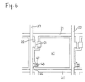
- Another conventional display device shown in Figure 6 comprises the TFT 31 formed over the gate bus branch 22 extended from the gate bus 21 including a portion of the gate bus branch 22 functioning as a gate electrode, as in the display device shown in Figure 4 .
- a redundant structure for short-circuiting the pixel electrode 41 with the source bus 23 is additionally formed.
- the redundant structure comprises an extrusion 46 extended from the source bus 23 , a conductive portion 47 overlapping the portion of the extrusion 46 , and a conductive piece 48 overlapthe conductive portion 47 and electrically connected to the pixel electrode 41 .
- Insulating films are interposed between the extrusion 46 and the conductive portion 47 and between the conductive portion 47 and the conductive piece 48 , so as to be insulated from each other.
- the detection of a point defect and correction of the defective pixel is performed as follows. At the stage that the substrate having the TFT 31 formed thereon and the counter substrate have been attached together with the liquid crystal sealed therebetween, appropriate signals are applied to gate buses 21 , source buses 23 and a counter electrode formed on the counter substrate, so as to detect any possible point defect by visual observation.
- part of an overlapping portion of the extrusion 46 of the source bus 23 and the conductive portion 47 and part of an overlapping portion of the conductive portion 47 and the conductive piece 48 are shot through by laser radiation through the transparent substrate.
- the extrusion 46 and the conductive portion 47 , and the conductive portion 47 and the conductive piece 48 are electrically connected.
- the conductive piece 48 has already been electrically connected to the pixel electrode 41 , the pixel electrode 41 can be short-circuited with the source bus 23 by the above-described laser radiation at two places, whereby the pixel electrode 41 can keep the same potential as the source signal.
- the point defect becomes unobtrusive, and thus the defective pixel can be corrected.
- the conventional display devices are constructed so that the pixel electrode 41 can be short-circuited with the source bus 23 through which signals are applied to the pixel electrode 41 , thereby to make a point defect unobtrusive and thus to correct the defective pixel.
- the correction of a leakage between the source bus 23 and the pixel electrode 41 may not be possible depending on the place where the leakage occurs.
- a leakage occurs between the pixel electrode 41 and the source bus 23 through which signals are applied to the pixel electrode 41 at a portion 81 shown by slant lines
- a current flows from the pixel electrode 41 to the source bus 23 when the TFT 31 is off.
- a pixel with the pixel electrode 41 is recognized as a point defect on the display.
- such a defective pixel can be corrected by short-circuiting the pixel electrode 41 with the source bus 23 by the laser radiation onto the TFT 31 as described above.
- EP-A-0 365 244 discloses an active matrix substrate according to the preamble of claim 1.
- EP-A-0 381 428 discloses an active matrix substrate according to the preamble of claim 5.
- this invention provides the active matrix display substrate having a pixel defect-repaired structure, as defined by claim 1, and the method of repairing an active matrix display substrate by forming such a pixel defect-repaired structure, as defined by claim 4.
- the sub-claims 2 and 3 are directed to embodiments of the invention.
- this invention provides the active matrix display substrate having a pixel defect-repaired structure, as defined by claim 5.
- the present invention makes possible achieving the objectives of providing an active matrix display device capable of (1) easily correcting a defective pixel and (2) preventing an occurrence of a line defect.
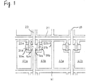
- an active matrix display device comprises a pair of transparent insulating substrates 1 and 2 and a liquid crystal 18 sealed therebetween.
- a plurality of gate buses 21 which function as scanning lines and a plurality of source buses 23 which function as signal lines are formed so as to cross each other.
- Two pixel electrodes 41a and 41b are disposed in each rectangular area defined by the adjacent gate buses 21 and the adjacent source buses 23 , and thus a plurality of pixel electrodes 41a and 41b are arranged in a matrix.
- Gate bus branches 22a and 22b are formed as extensions of the gate bus 21 , and over the end portions of the gate bus branches 22a and 22b including the end portions thereof functioning as gate electrodes, TFTs 31a and 31b are formed as switching elements, respectively.
- the portions of the gate bus branches 22a and 22b between the branch points from the gate bus 21 and the portions where the TFTs 31a and 31b are formed have a width narrow enough to be easily cut by radiation of a light energy, preferably a width of 5 to 15 ⁇ m. In this example, the width was 10 ⁇ m.
- the TFTs 31a and 31b are connected to the pixel electrodes 41a and 41b , respectively.
- a signal passing in one of the source buses 23 is applied to the pixel electrodes 41a and 41b disposed across the source bus 23 through the corresponding TFTs 31a and 31b .
- the pixel electrodes 41a and 41b adjacent to each other with the source bus 23 interposed therebetween constitute a pair of pixel electrodes which provide the same display.
- FIG. 2 is a sectional view taken along a line A - A in Figure 1 .
- metal such as Ta, Ti, Al and Cr was first deposited in a single layer or in multiple layers on the transparent insulating substrate 1 by a sputtering method and then patterned to form the gate bus 21 .
- the gate bus branch 22a ( 22b ) was also formed simultaneously with the gate bus 21 .
- glass was used for the transparent insulating substrate 1 .
- An insulating film made of Ta 2 O 5 , etc. may be formed as a base coat film under the gate bus 21 .
- a gate insulating film 13 was formed over the gate bus 21 and the gate bus branch 22a ( 22b ).
- SiN X was deposited to a thickness of 300 nm as the gate insulating film 13 by a plasma CVD method.
- an oxide film 12 may be formed by anodic oxidation of the gate bus 21 .
- the oxide film 12 made of Ta 2 O 5 will be formed.
- a semiconductor layer 14 and an etching stopper layer 15 were consecutively formed on the gate insulating film 13 .
- the semiconductor layer 14 was formed by depositing amorphous silicon (a-Si) to a thickness of 30 nm by the plasma CVD method and patterning, and the etching stopper layer 15 was formed by depositing SiN X to a thickness of 200 nm by the plasma CVD method and patterning. Then, silicon with phosphorus added thereto was deposited over the above layers to a thickness of 80 nm by the plasma CVD method and patterned to form an n + -type a-Si layer 16 .
- a-Si amorphous silicon
- n + -type a-Si layer 16 was formed to provide a favorable ohmic contact of the semiconductor layer 14 with a source electrode 32a ( 32b ) and a drain electrode 33a ( 33b ) to be formed on the n + -type a-Si layer 16 .
- Ti was used. In this way, the TFT 31 having the structure as shown in Figure 2 was formed.
- a transparent conductive substance was deposited by the sputtering method and patterned to form the pixel electrode 41a ( 41b ).
- ITO indium tin oxide
- two pixel electrodes 41a and 41b are formed in each rectangular area defined by the adjacent gate buses 21 and the adjacent source buses 23 , and the pixel electrodes 41a and 41b adjacent to each other with the source bus 23 therebetween constitute a pair of pixel electrodes effecting the same display.
- the end portion of the pixel electrode 41a ( 41b ) was formed to overlap the end portion of the drain electrode 33a ( 33b ) of the TFT 31a ( 31b ), so that the pixel electrode 41a ( 41b ) is electrically connected to the drain electrode 33a ( 33b ).
- SiN X was deposited over the entire surface of the glass substrate 1 on which the pixel electrode 41a ( 41b ) had been formed, so as to form a protective film 17 .
- the protective film 17 may be partly removed in the portion corresponding to the center portion of the pixel electrode 41a ( 41b ) to form a window.
- An orientation film 19 was then formed on the protective film 17 .
- the orientation film 19 may also be partly removed in the portion corresponding to the center portion of the pixel electrode 41a ( 41b ).
- a counter electrode 3 and an orientation film 9 were formed on the glass substrate 2 facing the glass substrate 1 . These glass substrates 1 and 2 were attached together with the liquid crystal 18 sealed therebetween, thus completing the active matrix display device of this example.
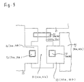
- each of the pixel electrodes 41a and 41b has only one source bus 23 formed on one side thereof through which signals are applied thereto, not having two source buses 23 on both sides thereof as the conventional display devices. Therefore, a line defect will not be produced by the laser processing on the TFT 31a or 31b to correct a defective pixel.
- the correction of the defective pixel can be made as in the conventional procedure shown in Figure 5 . That is, a YAG laser light, for example, is radiated to an area 51a ( 51b ) enclosed by a double line so as to disperse the metal of the narrow portion of the gate bus branch 22a ( 22b ). In this way, the gate bus 21 and the gate bus branch 22a ( 22b ) are electrically disconnected from each other.
- the laser light is radiated to an area 52a ( 52b ) enclosed by a double line, so as to break the source electrode 32a ( 32b ), the gate bus branch 22a ( 22b ) which is a gate electrode of the TFT 31a ( 31b ), and the gate insulating film 13 formed therebetween within the area 52a ( 52b ), thereby short-circuiting the source electrode 32a ( 32b ) with the gate electrode of the TFT 31a ( 31b ).
- the laser light is radiated to an area 53a ( 53b ) enclosed by a double line, so as to break the drain electrode 33a ( 33b ), the gate bus branch 22a ( 22b ) which is a gate electrode of the TFT 31a ( 31b ), and the gate insulating film 13 formed therebetween within the area 53a ( 53b ), thereby short-circuiting the drain electrode 33a ( 33b ) with the gate electrode of the TFT 31a ( 31b ).
- the pixel electrode 41a ( 41b ) can keep the same potential as the source signal.
- the defective pixel can be lightened to an average brightness of all pixels, and therefore the point defect becomes unobtrusive on the display.
- the defective pixel can be corrected.
- the order of the laser radiation to the areas 51a ( 51b ), 52a ( 52b ), and 53a ( 53b ) is not limited to that described above. Also, the positions of the areas 51a ( 51b ), 52a ( 52b ), and 53a ( 53b ) are not limited to those shown in Figure 5. For example, the areas 52a ( 52b ) and 53a ( 53b ) can be any portion where the conductive metals overlap each other.
- the laser radiation can be made either from the side of the substrate 1 where the TFTs 31a and 31b are formed or from the side of the substrate 2 where the counter electrode is formed.
- the laser radiation since the surface of the substrate 2 is covered with a light-shading metal blocking direct radiation of the laser light, the laser radiation was made from the side of substrate 1 .
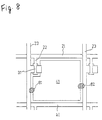
- a second example of the active matrix display device according to the present invention has the same structure as that of Example 1, except for an additional redundant structure which is disposed on corner portions of the pixel electrodes 41a and 41b for the specific purpose of short-circuiting the pixel electrodes 41a and 41b with the source bus 23 .
- the gate bus branches 22a and 22b of this example have a uniform width throughout the length thereof. This is because, in this example, it is not necessary to cut a portion of the gate bus branches 22a and 22b since the pixel electrodes 41a and 41b are provided with the redundant structure.
- the redundant structure comprises extrusions 46a and 46b extruding to the opposite sides from the source bus 23 , conductive portions 47a and 47b formed to overlap the portion of the extrusions 46a and 46b with an insulating film therebetween, respectively, and conductive pieces 48a and 48b formed to overlap the conductive portions 47a and 47b and electrically connected to the pixel electrodes 41a and 41b with an insulating film therebetween, respectively.
- each of the pixel electrodes 41a and 41b has only one source bus 23 formed on one side thereof through which signals are applied thereto. Therefore, a line defect will not be produced by laser processing on the TFT 31a or 31b to correct a defective pixel. When a point defect occurs, the correction can be made by laser processing of the redundant structure.
- part of an overlapping portion of the extrusion 46a ( 46b ) of the source bus 23 and the conductive portion 47a ( 47b ), shown as an area 54a ( 54b ) enclosed by a double line, is irradiated with laser light through the transparent substrate so as to break the extrusion 46a ( 46b ), the conductive portion 47a ( 47b ), and the insulating film therebetween within the area 54a ( 54b ), thereby short-circuiting the extrusion 46a ( 46b ) with the conductive portion 47a ( 47b ).
- the pixel electrode 41a ( 41b ) can be short-circuited with the source bus 23 by the above laser radiation at two places, thereby keeping the same potential as the source signal.
- the defective pixel can be lightened to an average brightness of all pixels, and therefore the point defect becomes unobtrusive on the display.
- the defective pixel can be corrected.
- the order of the laser radiation to the areas 54a ( 54b ) and 55a ( 55b ) is not limited to that described above. Also, the positions of the areas 54a ( 54b ) and 55a ( 55b ) are not limited to those shown in Figure 7 .
- the areas 54a ( 54b ) and 55a ( 55b ) can be any portion where the conductive metals overlap each other.
- the present invention is also applicable to a display device provided with an additional capacitance electrode.
- the switching element which drives the pixel electrode is not limited to the TFT, but other elements such as MIM elements, MOS transistors, diodes, and varistors can also be used.
- the structure of the TFT is not limited to that of the above examples, but the source bus can be formed on a lower position than the gate bus.
- each pixel electrode is provided between the adjacent signal lines, and two pixel electrodes adjacent to each other with each signal line therebetween are paired.
- the paired pixel electrodes are connected to respective switching elements which are connected to the common scanning line and the common signal line.
- each pixel electrode has only one signal line adjacent thereto.
- a portion of the scanning line branch between the branch point from the scanning line and the switching element is irradiated with a light energy to cut the portion, thereby electrically disconnecting the pixel electrode from the scanning line.
- part of the overlapping portion of the signal electrode extended from the signal line and the scanning line branch with the insulating film therebetween, and part of the overlapping portion of the scanning line branch and the electrode portion constituting the switching element and electrically connected to the pixel electrode with the insulating film therebetween are short-circuited.
- the pixel electrode and the signal line through which signals are applied to the pixel electrode are electrically connected, whereby the defective pixel can be corrected.
- a leakage between the signal lines will not occur, and therefore an occurrence of a line defect is prevented.
- the scanning line and the switching element can be easily electrically disconnected.
- the display device comprising the redundant structure
- part of the overlapping portion of the conductive portion and the signal line with the insulating film therebetween and part of the overlapping portion of the conductive portion and the conductive piece electrically connecting to the pixel electrode with the insulating film therebetween are short-circuited.
- the pixel electrode and the signal line through which signals are applied to the pixel electrode are electrically connected without intervention of the switching element, thereby allowing a defective pixel to be corrected. Therefore, according to the present invention, the display devices can be manufactured with a high yield, thereby reducing the manufacturing cost.
Landscapes
- Physics & Mathematics (AREA)
- Nonlinear Science (AREA)
- Engineering & Computer Science (AREA)
- Microelectronics & Electronic Packaging (AREA)
- Mathematical Physics (AREA)
- Chemical & Material Sciences (AREA)
- Crystallography & Structural Chemistry (AREA)
- General Physics & Mathematics (AREA)
- Optics & Photonics (AREA)
- Liquid Crystal (AREA)
- Thin Film Transistor (AREA)
- Devices For Indicating Variable Information By Combining Individual Elements (AREA)
Applications Claiming Priority (2)
| Application Number | Priority Date | Filing Date | Title |
|---|---|---|---|
| JP102365/91 | 1991-05-08 | ||
| JP10236591A JP2669954B2 (ja) | 1991-05-08 | 1991-05-08 | アクティブマトリクス表示装置 |
Publications (3)
| Publication Number | Publication Date |
|---|---|
| EP0512840A2 EP0512840A2 (en) | 1992-11-11 |
| EP0512840A3 EP0512840A3 (en) | 1993-02-24 |
| EP0512840B1 true EP0512840B1 (en) | 1997-07-30 |
Family
ID=14325439
Family Applications (1)
| Application Number | Title | Priority Date | Filing Date |
|---|---|---|---|
| EP92304133A Expired - Lifetime EP0512840B1 (en) | 1991-05-08 | 1992-05-08 | An active matrix display device |
Country Status (6)
| Country | Link |
|---|---|
| US (1) | US5434686A (enExample) |
| EP (1) | EP0512840B1 (enExample) |
| JP (1) | JP2669954B2 (enExample) |
| KR (1) | KR920022028A (enExample) |
| DE (1) | DE69221201T2 (enExample) |
| TW (1) | TW235375B (enExample) |
Families Citing this family (23)
| Publication number | Priority date | Publication date | Assignee | Title |
|---|---|---|---|---|
| JPH0675203A (ja) * | 1992-08-26 | 1994-03-18 | Sharp Corp | 表示装置の駆動回路 |
| US5774099A (en) * | 1995-04-25 | 1998-06-30 | Hitachi, Ltd. | Liquid crystal device with wide viewing angle characteristics |
| KR0182014B1 (ko) * | 1995-08-23 | 1999-05-01 | 김광호 | 액정 표시 장치용 박막트랜지스터 기판 |
| US5995178A (en) * | 1995-10-16 | 1999-11-30 | Sharp Kabushiki Kaisha | Active matrix liquid crystal panel and method for repairing defect therein |
| TW531686B (en) | 1997-04-11 | 2003-05-11 | Hitachi Ltd | Liquid crystal display device |
| JP3966614B2 (ja) | 1997-05-29 | 2007-08-29 | 三星電子株式会社 | 広視野角液晶表示装置 |
| KR100590741B1 (ko) * | 1998-04-03 | 2006-09-18 | 삼성전자주식회사 | 액정 표시 장치 |
| KR100354904B1 (ko) | 1998-05-19 | 2002-12-26 | 삼성전자 주식회사 | 광시야각액정표시장치 |
| KR100336888B1 (ko) * | 1998-09-07 | 2003-06-12 | 주식회사 현대 디스플레이 테크놀로지 | 액정표시소자 |
| JP3450195B2 (ja) * | 1998-09-07 | 2003-09-22 | 富士通ディスプレイテクノロジーズ株式会社 | 液晶表示装置及びその修復方法 |
| US7280090B2 (en) * | 2000-12-22 | 2007-10-09 | Electronics For Imaging, Inc. | Methods and apparatus for repairing inoperative pixels in a display |
| US6855937B2 (en) * | 2001-05-18 | 2005-02-15 | Canon Kabushiki Kaisha | Image pickup apparatus |
| JP4248306B2 (ja) | 2002-06-17 | 2009-04-02 | シャープ株式会社 | 液晶表示装置 |
| KR100840326B1 (ko) | 2002-06-28 | 2008-06-20 | 삼성전자주식회사 | 액정 표시 장치 및 그에 사용되는 박막 트랜지스터 기판 |
| JP2004038041A (ja) * | 2002-07-05 | 2004-02-05 | Chi Mei Electronics Corp | 画像表示素子及び画像表示装置 |
| WO2004068446A1 (ja) * | 2003-01-27 | 2004-08-12 | Toshiba Matsushita Display Technology Co., Ltd. | 有機elディスプレイの製造方法 |
| KR100569718B1 (ko) * | 2003-05-20 | 2006-04-10 | 삼성전자주식회사 | 다중 도메인 액정 표시 장치 |
| US7206048B2 (en) * | 2003-08-13 | 2007-04-17 | Samsung Electronics Co., Ltd. | Liquid crystal display and panel therefor |
| JP2007003709A (ja) * | 2005-06-22 | 2007-01-11 | Sharp Corp | アクティブマトリクス基板、表示装置およびその欠陥修正方法 |
| US8592262B2 (en) * | 2006-11-16 | 2013-11-26 | Au Optronics Corporation | Residue isolation process in TFT LCD fabrication |
| CN102759833B (zh) * | 2012-07-27 | 2015-05-20 | 京东方科技集团股份有限公司 | 一种阵列基板及显示装置 |
| WO2016002576A1 (ja) * | 2014-07-03 | 2016-01-07 | ソニー株式会社 | 固体撮像素子、および電子装置 |
| CN105954950A (zh) * | 2016-07-07 | 2016-09-21 | 深圳市华星光电技术有限公司 | 一种阵列基板及阵列基板的扫描线修补方法 |
Family Cites Families (19)
| Publication number | Priority date | Publication date | Assignee | Title |
|---|---|---|---|---|
| US4775861A (en) * | 1984-11-02 | 1988-10-04 | Nec Corporation | Driving circuit of a liquid crystal display panel which equivalently reduces picture defects |
| DE3581498D1 (de) * | 1984-11-16 | 1991-02-28 | Matsushita Electric Industrial Co Ltd | Aktive matrixschaltung fuer fluessigkristallanzeigen. |
| FR2581783B1 (fr) * | 1985-05-07 | 1989-05-12 | Commissariat Energie Atomique | Dispositif d'affichage a matrice active et a commande integree comprenant deux familles d'electrodes lignes et deux familles d'electrodes colonnes par point image et son procede de commande |
| JPS63262621A (ja) * | 1987-04-21 | 1988-10-28 | Alps Electric Co Ltd | 薄膜トランジスタアレイのトリミング方法 |
| DE68923146T2 (de) * | 1988-10-17 | 1995-11-30 | Sharp Kk | Substrat mit einer aktiven Matrix. |
| JPH02124538A (ja) * | 1988-11-02 | 1990-05-11 | Fujitsu Ltd | アクティブマトリクス型液晶表示装置 |
| US5076666A (en) * | 1988-12-06 | 1991-12-31 | Sharp Kabushiki Kaisha | Active matrix display apparatus with drain electrode extensions |
| US4968119A (en) * | 1989-01-10 | 1990-11-06 | David Sarnoff Research Center, Inc. | High-density liquid-crystal active dot-matrix display structure |
| US5151807A (en) * | 1989-01-31 | 1992-09-29 | Sharp Kabushiki Kaisha | Active matrix substrate and active matrix display apparatus |
| JPH0324524A (ja) * | 1989-06-21 | 1991-02-01 | Sharp Corp | アクティブマトリクス表示装置 |
| US5343216A (en) * | 1989-01-31 | 1994-08-30 | Sharp Kabushiki Kaisha | Active matrix substrate and active matrix display apparatus |
| JPH02251930A (ja) * | 1989-03-27 | 1990-10-09 | Matsushita Electric Ind Co Ltd | アクティブマトリックスアレイ |
| JPH0333724A (ja) * | 1989-06-30 | 1991-02-14 | Hitachi Ltd | 液晶表示装置 |
| US5062690A (en) * | 1989-06-30 | 1991-11-05 | General Electric Company | Liquid crystal display with redundant FETS and redundant crossovers connected by laser-fusible links |
| JPH0820644B2 (ja) * | 1989-09-19 | 1996-03-04 | シャープ株式会社 | マトリクス型液晶表示基板の製造方法 |
| JPH0820646B2 (ja) * | 1990-05-11 | 1996-03-04 | シャープ株式会社 | アクティブマトリクス型表示装置 |
| JPH07122719B2 (ja) * | 1990-05-11 | 1995-12-25 | シャープ株式会社 | アクティブマトリクス型表示装置 |
| JPH0830826B2 (ja) * | 1990-05-14 | 1996-03-27 | シャープ株式会社 | アクティブマトリクス型表示装置の製造方法 |
| JPH0421823A (ja) * | 1990-05-16 | 1992-01-24 | Hosiden Corp | 液晶表示素子の点欠陥の黒欠陥化法及び液晶表示素子 |
-
1991
- 1991-05-08 JP JP10236591A patent/JP2669954B2/ja not_active Expired - Lifetime
-
1992
- 1992-05-07 TW TW081103574A patent/TW235375B/zh active
- 1992-05-08 DE DE69221201T patent/DE69221201T2/de not_active Expired - Fee Related
- 1992-05-08 EP EP92304133A patent/EP0512840B1/en not_active Expired - Lifetime
- 1992-05-08 KR KR1019920007819A patent/KR920022028A/ko not_active Ceased
-
1993
- 1993-09-09 US US08/123,847 patent/US5434686A/en not_active Expired - Fee Related
Also Published As
| Publication number | Publication date |
|---|---|
| DE69221201T2 (de) | 1998-02-05 |
| KR920022028A (ko) | 1992-12-19 |
| DE69221201D1 (de) | 1997-09-04 |
| EP0512840A3 (en) | 1993-02-24 |
| JPH04331922A (ja) | 1992-11-19 |
| TW235375B (enExample) | 1994-12-01 |
| EP0512840A2 (en) | 1992-11-11 |
| US5434686A (en) | 1995-07-18 |
| JP2669954B2 (ja) | 1997-10-29 |
Similar Documents
| Publication | Publication Date | Title |
|---|---|---|
| EP0512840B1 (en) | An active matrix display device | |
| EP0456338B1 (en) | An active matrix display device and a method of manufacturing the same | |
| US5469025A (en) | Fault tolerant active matrix display device | |
| EP0441595B1 (en) | An active matrix display device | |
| EP0484842B1 (en) | Flat panel display | |
| US5686977A (en) | Liquid crystal display and a manufacturing method thereof | |
| EP0766118B1 (en) | Active-matrix type liquid crystal display device | |
| KR960014823B1 (ko) | 액정표시장치 | |
| JP4636820B2 (ja) | 薄膜トランジスタ表示板及びこれを含む液晶表示装置の修理方法 | |
| EP0381428B1 (en) | Active matrix substrate and active matrix display display apparatus | |
| US6191832B1 (en) | Active matrix display device and methods for correcting defect thereof | |
| US5343216A (en) | Active matrix substrate and active matrix display apparatus | |
| US6985194B2 (en) | Matrix array substrate | |
| EP0482737B1 (en) | Active matrix display device | |
| RU2441263C1 (ru) | Подложка активной матрицы, панель жидкокристаллического дисплея, оборудованная ею, и способ производства подложки активной матрицы | |
| JP2760459B2 (ja) | アクティブマトリクス型基板 | |
| JPH0820646B2 (ja) | アクティブマトリクス型表示装置 | |
| JPH06289426A (ja) | アクティブマトリクス表示装置の修正方法 | |
| JP3418684B2 (ja) | アクティブマトリクス型液晶表示装置 | |
| US6341005B1 (en) | Method for producing liquid crystal device with conductors arranged in a matrix | |
| KR950004218B1 (ko) | 매트릭스 어드레스 표시장치 및 그 제조방법 | |
| JP3418683B2 (ja) | アクティブマトリクス型液晶表示装置 | |
| JPH0748146B2 (ja) | アクティブマトリクス基板及びアクティブマトリクス表示装置 | |
| KR20020039086A (ko) | 액정표시패널의 데이터배선 결함보정구조와 그 결합보정방법 | |
| JPH0534719A (ja) | アクテイブマトリクス表示装置 |
Legal Events
| Date | Code | Title | Description |
|---|---|---|---|
| PUAI | Public reference made under article 153(3) epc to a published international application that has entered the european phase |
Free format text: ORIGINAL CODE: 0009012 |
|
| AK | Designated contracting states |
Kind code of ref document: A2 Designated state(s): DE FR GB NL |
|
| PUAL | Search report despatched |
Free format text: ORIGINAL CODE: 0009013 |
|
| AK | Designated contracting states |
Kind code of ref document: A3 Designated state(s): DE FR GB NL |
|
| 17P | Request for examination filed |
Effective date: 19930415 |
|
| 17Q | First examination report despatched |
Effective date: 19941202 |
|
| GRAG | Despatch of communication of intention to grant |
Free format text: ORIGINAL CODE: EPIDOS AGRA |
|
| GRAH | Despatch of communication of intention to grant a patent |
Free format text: ORIGINAL CODE: EPIDOS IGRA |
|
| GRAH | Despatch of communication of intention to grant a patent |
Free format text: ORIGINAL CODE: EPIDOS IGRA |
|
| GRAA | (expected) grant |
Free format text: ORIGINAL CODE: 0009210 |
|
| AK | Designated contracting states |
Kind code of ref document: B1 Designated state(s): DE FR GB NL |
|
| REF | Corresponds to: |
Ref document number: 69221201 Country of ref document: DE Date of ref document: 19970904 |
|
| ET | Fr: translation filed | ||
| PLBE | No opposition filed within time limit |
Free format text: ORIGINAL CODE: 0009261 |
|
| STAA | Information on the status of an ep patent application or granted ep patent |
Free format text: STATUS: NO OPPOSITION FILED WITHIN TIME LIMIT |
|
| 26N | No opposition filed | ||
| REG | Reference to a national code |
Ref country code: GB Ref legal event code: IF02 |
|
| PGFP | Annual fee paid to national office [announced via postgrant information from national office to epo] |
Ref country code: GB Payment date: 20020508 Year of fee payment: 11 Ref country code: FR Payment date: 20020508 Year of fee payment: 11 |
|
| PGFP | Annual fee paid to national office [announced via postgrant information from national office to epo] |
Ref country code: DE Payment date: 20020516 Year of fee payment: 11 |
|
| PGFP | Annual fee paid to national office [announced via postgrant information from national office to epo] |
Ref country code: NL Payment date: 20020529 Year of fee payment: 11 |
|
| PG25 | Lapsed in a contracting state [announced via postgrant information from national office to epo] |
Ref country code: GB Free format text: LAPSE BECAUSE OF NON-PAYMENT OF DUE FEES Effective date: 20030508 |
|
| PG25 | Lapsed in a contracting state [announced via postgrant information from national office to epo] |
Ref country code: NL Free format text: LAPSE BECAUSE OF NON-PAYMENT OF DUE FEES Effective date: 20031201 |
|
| PG25 | Lapsed in a contracting state [announced via postgrant information from national office to epo] |
Ref country code: DE Free format text: LAPSE BECAUSE OF NON-PAYMENT OF DUE FEES Effective date: 20031202 |
|
| GBPC | Gb: european patent ceased through non-payment of renewal fee |
Effective date: 20030508 |
|
| PG25 | Lapsed in a contracting state [announced via postgrant information from national office to epo] |
Ref country code: FR Free format text: LAPSE BECAUSE OF NON-PAYMENT OF DUE FEES Effective date: 20040130 |
|
| NLV4 | Nl: lapsed or anulled due to non-payment of the annual fee |
Effective date: 20031201 |
|
| REG | Reference to a national code |
Ref country code: FR Ref legal event code: ST |