EP0512296B1 - Hochtemperatur-Niederschlagsverfahren von Leitern in Öffnungen, die tiefer als breit sind - Google Patents
Hochtemperatur-Niederschlagsverfahren von Leitern in Öffnungen, die tiefer als breit sind Download PDFInfo
- Publication number
- EP0512296B1 EP0512296B1 EP92106614A EP92106614A EP0512296B1 EP 0512296 B1 EP0512296 B1 EP 0512296B1 EP 92106614 A EP92106614 A EP 92106614A EP 92106614 A EP92106614 A EP 92106614A EP 0512296 B1 EP0512296 B1 EP 0512296B1
- Authority
- EP
- European Patent Office
- Prior art keywords
- aspect ratio
- collimator
- titanium
- deposited
- tin
- Prior art date
- Legal status (The legal status is an assumption and is not a legal conclusion. Google has not performed a legal analysis and makes no representation as to the accuracy of the status listed.)
- Expired - Lifetime
Links
Images


Classifications
-
- H—ELECTRICITY
- H01—ELECTRIC ELEMENTS
- H01J—ELECTRIC DISCHARGE TUBES OR DISCHARGE LAMPS
- H01J37/00—Discharge tubes with provision for introducing objects or material to be exposed to the discharge, e.g. for the purpose of examination or processing thereof
- H01J37/32—Gas-filled discharge tubes
- H01J37/34—Gas-filled discharge tubes operating with cathodic sputtering
- H01J37/3411—Constructional aspects of the reactor
- H01J37/3447—Collimators, shutters, apertures
-
- C—CHEMISTRY; METALLURGY
- C23—COATING METALLIC MATERIAL; COATING MATERIAL WITH METALLIC MATERIAL; CHEMICAL SURFACE TREATMENT; DIFFUSION TREATMENT OF METALLIC MATERIAL; COATING BY VACUUM EVAPORATION, BY SPUTTERING, BY ION IMPLANTATION OR BY CHEMICAL VAPOUR DEPOSITION, IN GENERAL; INHIBITING CORROSION OF METALLIC MATERIAL OR INCRUSTATION IN GENERAL
- C23C—COATING METALLIC MATERIAL; COATING MATERIAL WITH METALLIC MATERIAL; SURFACE TREATMENT OF METALLIC MATERIAL BY DIFFUSION INTO THE SURFACE, BY CHEMICAL CONVERSION OR SUBSTITUTION; COATING BY VACUUM EVAPORATION, BY SPUTTERING, BY ION IMPLANTATION OR BY CHEMICAL VAPOUR DEPOSITION, IN GENERAL
- C23C14/00—Coating by vacuum evaporation, by sputtering or by ion implantation of the coating forming material
- C23C14/04—Coating on selected surface areas, e.g. using masks
-
- H—ELECTRICITY
- H01—ELECTRIC ELEMENTS
- H01J—ELECTRIC DISCHARGE TUBES OR DISCHARGE LAMPS
- H01J37/00—Discharge tubes with provision for introducing objects or material to be exposed to the discharge, e.g. for the purpose of examination or processing thereof
- H01J37/32—Gas-filled discharge tubes
- H01J37/34—Gas-filled discharge tubes operating with cathodic sputtering
-
- H—ELECTRICITY
- H10—SEMICONDUCTOR DEVICES; ELECTRIC SOLID-STATE DEVICES NOT OTHERWISE PROVIDED FOR
- H10W—GENERIC PACKAGES, INTERCONNECTIONS, CONNECTORS OR OTHER CONSTRUCTIONAL DETAILS OF DEVICES COVERED BY CLASS H10
- H10W20/00—Interconnections in chips, wafers or substrates
- H10W20/01—Manufacture or treatment
- H10W20/031—Manufacture or treatment of conductive parts of the interconnections
- H10W20/056—Manufacture or treatment of conductive parts of the interconnections by filling conductive material into holes, grooves or trenches
-
- H—ELECTRICITY
- H05—ELECTRIC TECHNIQUES NOT OTHERWISE PROVIDED FOR
- H05K—PRINTED CIRCUITS; CASINGS OR CONSTRUCTIONAL DETAILS OF ELECTRIC APPARATUS; MANUFACTURE OF ASSEMBLAGES OF ELECTRICAL COMPONENTS
- H05K3/00—Apparatus or processes for manufacturing printed circuits
- H05K3/40—Forming printed elements for providing electric connections to or between printed circuits
- H05K3/4038—Through-connections; Vertical interconnect access [VIA] connections
- H05K3/4076—Through-connections; Vertical interconnect access [VIA] connections by thin-film techniques
Definitions
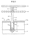
- the substrate temperature is maintained at 450°C, and argon is used as the inert bombardment atom.
- the ambient is changed to N2.
- the resulting composite film has portion 40C that is on the order or 260 angstroms (or roughly 25%) of the thickness of portions 40A.
- the sidewall portions 40B of the composite film have substantially uniform thickness along the entire contact hole sidewall, enhancing adhesion of subsequently-applied films.
Landscapes
- Chemical & Material Sciences (AREA)
- Engineering & Computer Science (AREA)
- Physics & Mathematics (AREA)
- Plasma & Fusion (AREA)
- Analytical Chemistry (AREA)
- Chemical Kinetics & Catalysis (AREA)
- Materials Engineering (AREA)
- Mechanical Engineering (AREA)
- Metallurgy (AREA)
- Organic Chemistry (AREA)
- Internal Circuitry In Semiconductor Integrated Circuit Devices (AREA)
- Electrodes Of Semiconductors (AREA)
Claims (4)
- Verfahren zur Abscheidung einer Schicht aus refraktärem Metall auf einem Substrat mit einer Oberflächentopographie mit mindestens einer horizontalen Oberfläche und mindestens einer Vertiefung mit einem Aspektverhältnis von etwa 1:1 oder mehr, bei dem man:Atome des refraktären Metalls vor der Abscheidung auf dem Substrat durch einen Kollimator mit Öffnungen mit einem Aspektverhältnis von etwa 1:1 oder mehr führt,während der Abscheidung das Substrat bei einer Temperatur von mindestens 450°C hält, so daß die Dicke der am Boden der Vertiefung abgeschiedenen Schicht im Verhältnis zur Dicke der auf der horizontalen Oberfläche des Substrats abgeschiedenen Schicht erhöht wird.
- Verfahren nach Anspruch 1, bei dem es sich bei dem Leiter um Titan oder Titanlegierungen handelt.
- Verfahren nach Anspruch 2, bei dem es sich bei der Titanlegierung um Titannitrid handelt.
- Verfahren nach einem der Ansprüche 1 bis 3, bei dem die Kollimatoröffnungen ein Aspektverhältnis von 2:1 haben.
Applications Claiming Priority (2)
| Application Number | Priority Date | Filing Date | Title |
|---|---|---|---|
| US68802091A | 1991-04-19 | 1991-04-19 | |
| US688020 | 1991-04-19 |
Publications (2)
| Publication Number | Publication Date |
|---|---|
| EP0512296A1 EP0512296A1 (de) | 1992-11-11 |
| EP0512296B1 true EP0512296B1 (de) | 1997-03-05 |
Family
ID=24762785
Family Applications (1)
| Application Number | Title | Priority Date | Filing Date |
|---|---|---|---|
| EP92106614A Expired - Lifetime EP0512296B1 (de) | 1991-04-19 | 1992-04-16 | Hochtemperatur-Niederschlagsverfahren von Leitern in Öffnungen, die tiefer als breit sind |
Country Status (5)
| Country | Link |
|---|---|
| US (1) | US5529670A (de) |
| EP (1) | EP0512296B1 (de) |
| JP (1) | JP2725944B2 (de) |
| DE (1) | DE69217702T2 (de) |
| IE (1) | IE80715B1 (de) |
Families Citing this family (40)
| Publication number | Priority date | Publication date | Assignee | Title |
|---|---|---|---|---|
| US6521106B1 (en) | 1990-01-29 | 2003-02-18 | Novellus Systems, Inc. | Collimated deposition apparatus |
| CA2111536A1 (en) * | 1992-12-16 | 1994-06-17 | Geri M. Actor | Collimated deposition apparatus |
| US5362372A (en) * | 1993-06-11 | 1994-11-08 | Applied Materials, Inc. | Self cleaning collimator |
| JPH0718423A (ja) * | 1993-07-06 | 1995-01-20 | Japan Energy Corp | 薄膜形成装置 |
| US5356836A (en) * | 1993-08-19 | 1994-10-18 | Industrial Technology Research Institute | Aluminum plug process |
| JP3398452B2 (ja) * | 1994-01-19 | 2003-04-21 | 株式会社ソニー・ディスクテクノロジー | スパッタリング装置 |
| JP2689931B2 (ja) * | 1994-12-29 | 1997-12-10 | 日本電気株式会社 | スパッタ方法 |
| US5757879A (en) * | 1995-06-07 | 1998-05-26 | International Business Machines Corporation | Tungsten absorber for x-ray mask |
| JPH0936228A (ja) * | 1995-07-21 | 1997-02-07 | Sony Corp | 配線形成方法 |
| JPH09102541A (ja) * | 1995-10-05 | 1997-04-15 | Mitsubishi Electric Corp | 半導体装置及びその製造方法 |
| DE19621855C2 (de) * | 1996-05-31 | 2003-03-27 | Univ Dresden Tech | Verfahren zur Herstellung von Metallisierungen auf Halbleiterkörpern unter Verwendung eines gepulsten Vakuumbogenverdampfers |
| US5801096A (en) * | 1996-06-03 | 1998-09-01 | Taiwan Semiconductor Manufacturing Company Ltd. | Self-aligned tungsen etch back process to minimize seams in tungsten plugs |
| JP2894279B2 (ja) * | 1996-06-10 | 1999-05-24 | 日本電気株式会社 | 金属薄膜形成方法 |
| JPH1012729A (ja) * | 1996-06-27 | 1998-01-16 | Nec Corp | 半導体装置の製造方法 |
| KR100206938B1 (ko) * | 1996-09-19 | 1999-07-01 | 구본준 | 반도체 제조장치 및 이를 이용한 반도체 소자의 배선 형성방법 |
| US5783282A (en) * | 1996-10-07 | 1998-07-21 | Micron Technology, Inc. | Resputtering to achieve better step coverage of contact holes |
| JPH10237662A (ja) * | 1996-12-24 | 1998-09-08 | Sony Corp | 金属膜のプラズマcvd方法、および金属窒化物膜の形成方法ならびに半導体装置 |
| US6168832B1 (en) | 1997-01-20 | 2001-01-02 | Coherent, Inc. | Three-dimensional masking method for control of coating thickness |
| GB9701114D0 (en) * | 1997-01-20 | 1997-03-12 | Coherent Optics Europ Ltd | Three-dimensional masking method for control of optical coating thickness |
| US6605197B1 (en) * | 1997-05-13 | 2003-08-12 | Applied Materials, Inc. | Method of sputtering copper to fill trenches and vias |
| US6045634A (en) * | 1997-08-14 | 2000-04-04 | Praxair S. T. Technology, Inc. | High purity titanium sputtering target and method of making |
| US6277737B1 (en) | 1998-09-02 | 2001-08-21 | Micron Technology, Inc. | Semiconductor processing methods and integrated circuitry |
| JP3358587B2 (ja) | 1999-05-26 | 2002-12-24 | 日本電気株式会社 | 半導体装置の製造方法 |
| GB2357371B (en) | 1999-11-04 | 2004-02-11 | Trikon Holdings Ltd | A method of forming a barrier layer |
| JP2002069634A (ja) * | 2000-08-29 | 2002-03-08 | Canon Inc | 薄膜作製方法および薄膜作製装置 |
| JP2002217292A (ja) | 2001-01-23 | 2002-08-02 | Hitachi Ltd | 半導体集積回路装置および半導体集積回路装置の製造方法 |
| US7355687B2 (en) * | 2003-02-20 | 2008-04-08 | Hunter Engineering Company | Method and apparatus for vehicle service system with imaging components |
| US7070697B2 (en) * | 2003-04-14 | 2006-07-04 | Hitachi Global Storage Technologies Netherlands B.V. | Methods of making a read sensor with use of a barrier structure for depositing materials |
| US7291360B2 (en) * | 2004-03-26 | 2007-11-06 | Applied Materials, Inc. | Chemical vapor deposition plasma process using plural ion shower grids |
| US20050211546A1 (en) * | 2004-03-26 | 2005-09-29 | Applied Materials, Inc. | Reactive sputter deposition plasma process using an ion shower grid |
| US20050211547A1 (en) * | 2004-03-26 | 2005-09-29 | Applied Materials, Inc. | Reactive sputter deposition plasma reactor and process using plural ion shower grids |
| US7244474B2 (en) * | 2004-03-26 | 2007-07-17 | Applied Materials, Inc. | Chemical vapor deposition plasma process using an ion shower grid |
| US7695590B2 (en) | 2004-03-26 | 2010-04-13 | Applied Materials, Inc. | Chemical vapor deposition plasma reactor having plural ion shower grids |
| US7767561B2 (en) * | 2004-07-20 | 2010-08-03 | Applied Materials, Inc. | Plasma immersion ion implantation reactor having an ion shower grid |
| US8058156B2 (en) * | 2004-07-20 | 2011-11-15 | Applied Materials, Inc. | Plasma immersion ion implantation reactor having multiple ion shower grids |
| US7407875B2 (en) * | 2006-09-06 | 2008-08-05 | International Business Machines Corporation | Low resistance contact structure and fabrication thereof |
| JP2007295004A (ja) * | 2007-07-27 | 2007-11-08 | Toshiba Corp | 半導体装置の製造方法 |
| JP5145000B2 (ja) * | 2007-09-28 | 2013-02-13 | 株式会社フジクラ | 貫通配線基板、半導体パッケージ及び貫通配線基板の製造方法 |
| JP2009182140A (ja) * | 2008-01-30 | 2009-08-13 | Tokyo Electron Ltd | 薄膜の形成方法、プラズマ成膜装置及び記憶媒体 |
| TW201005109A (en) * | 2008-07-25 | 2010-02-01 | Inotera Memories Inc | Method for changing physical vapor deposition film form |
Family Cites Families (18)
| Publication number | Priority date | Publication date | Assignee | Title |
|---|---|---|---|---|
| US4293374A (en) * | 1980-03-10 | 1981-10-06 | International Business Machines Corporation | High aspect ratio, high resolution mask fabrication |
| KR900001825B1 (ko) * | 1984-11-14 | 1990-03-24 | 가부시끼가이샤 히다찌세이사꾸쇼 | 성막 지향성을 고려한 스퍼터링장치 |
| FR2583220B1 (fr) * | 1985-06-11 | 1987-08-07 | Thomson Csf | Procede de realisation d'au moins deux metallisations d'un composant semi-conducteur, recouvertes d'une couche de dielectrique et composant obtenu par ce dielectrique |
| JPS627855A (ja) * | 1985-07-05 | 1987-01-14 | Hitachi Ltd | スパツタリング装置 |
| JPS6217173A (ja) * | 1985-07-15 | 1987-01-26 | Ulvac Corp | 平板マグネトロンスパツタ装置 |
| JPH084088B2 (ja) * | 1986-02-27 | 1996-01-17 | 工業技術院長 | 薄膜形成方法 |
| US4756810A (en) * | 1986-12-04 | 1988-07-12 | Machine Technology, Inc. | Deposition and planarizing methods and apparatus |
| US4783248A (en) * | 1987-02-10 | 1988-11-08 | Siemens Aktiengesellschaft | Method for the production of a titanium/titanium nitride double layer |
| JPH0660391B2 (ja) * | 1987-06-11 | 1994-08-10 | 日電アネルバ株式会社 | スパッタリング装置 |
| US4824544A (en) * | 1987-10-29 | 1989-04-25 | International Business Machines Corporation | Large area cathode lift-off sputter deposition device |
| JP2776826B2 (ja) * | 1988-04-15 | 1998-07-16 | 株式会社日立製作所 | 半導体装置およびその製造方法 |
| US4822753A (en) * | 1988-05-09 | 1989-04-18 | Motorola, Inc. | Method for making a w/tin contact |
| JPH02178923A (ja) * | 1988-12-29 | 1990-07-11 | Fujitsu Ltd | 半導体装置の製造方法 |
| US4920073A (en) * | 1989-05-11 | 1990-04-24 | Texas Instruments, Incorporated | Selective silicidation process using a titanium nitride protective layer |
| US4994162A (en) * | 1989-09-29 | 1991-02-19 | Materials Research Corporation | Planarization method |
| US5026470A (en) * | 1989-12-19 | 1991-06-25 | International Business Machines | Sputtering apparatus |
| EP0440377B1 (de) * | 1990-01-29 | 1998-03-18 | Varian Associates, Inc. | Gerät und Verfahren zur Niederschlagung durch einen Kollimator |
| US5008217A (en) * | 1990-06-08 | 1991-04-16 | At&T Bell Laboratories | Process for fabricating integrated circuits having shallow junctions |
-
1992
- 1992-03-26 JP JP4102200A patent/JP2725944B2/ja not_active Expired - Fee Related
- 1992-04-16 DE DE69217702T patent/DE69217702T2/de not_active Expired - Fee Related
- 1992-04-16 IE IE921253A patent/IE80715B1/en not_active IP Right Cessation
- 1992-04-16 EP EP92106614A patent/EP0512296B1/de not_active Expired - Lifetime
-
1993
- 1993-12-22 US US08/172,017 patent/US5529670A/en not_active Expired - Lifetime
Also Published As
| Publication number | Publication date |
|---|---|
| JPH06140359A (ja) | 1994-05-20 |
| US5529670A (en) | 1996-06-25 |
| IE80715B1 (en) | 1998-12-30 |
| EP0512296A1 (de) | 1992-11-11 |
| DE69217702D1 (de) | 1997-04-10 |
| JP2725944B2 (ja) | 1998-03-11 |
| DE69217702T2 (de) | 1997-10-23 |
| IE921253A1 (en) | 1992-10-21 |
Similar Documents
| Publication | Publication Date | Title |
|---|---|---|
| US5529670A (en) | Method of depositing conductors in high aspect ratio apertures under high temperature conditions | |
| US5401675A (en) | Method of depositing conductors in high aspect ratio apertures using a collimator | |
| JP3094004B2 (ja) | 半導体ウェーハ上へのタングステン層のcvd蒸着方法 | |
| KR100717086B1 (ko) | 화학 기상 증착에 의해 증착된 구리의 밀착성을 강화하기위한 방법 | |
| US6258710B1 (en) | Sub-quarter-micron copper interconnections with improved electromigration resistance and reduced defect sensitivity | |
| US6458684B1 (en) | Single step process for blanket-selective CVD aluminum deposition | |
| US6399490B1 (en) | Highly conformal titanium nitride deposition process for high aspect ratio structures | |
| US5882399A (en) | Method of forming a barrier layer which enables a consistently highly oriented crystalline structure in a metallic interconnect | |
| Raaijmakers | Low temperature metal-organic chemical vapor deposition of advanced barrier layers for the microelectronics industry | |
| EP0794568A2 (de) | CVD nicht selektive/selektive Aluminiumabscheidung und Reflektivitätsverbesserung unter Verwendung von einer selbstjustierenden ultradünnen Schicht | |
| US6110828A (en) | In-situ capped aluminum plug (CAP) process using selective CVD AL for integrated plug/interconnect metallization | |
| KR19980080279A (ko) | 알루미늄 플러그용 실리콘 도핑 티타늄 습식층 | |
| Mehrotra et al. | Properties of direct current magnetron reactively sputtered TaN | |
| US20020093101A1 (en) | Method of metallization using a nickel-vanadium layer | |
| US6156647A (en) | Barrier layer structure which prevents migration of silicon into an adjacent metallic layer and the method of fabrication of the barrier layer | |
| KR20030020986A (ko) | 스퍼터링 타겟 | |
| JP3315211B2 (ja) | 電子部品 | |
| Cerio et al. | Film properties of Ti/TiN bilayers deposited sequentially by ionized physical vapor deposition | |
| KR19990013553A (ko) | 반도체 디바이스 및 반도체 디바이스 제조 공정 | |
| US6245668B1 (en) | Sputtered tungsten diffusion barrier for improved interconnect robustness | |
| US6107195A (en) | Method for depositing a low-resistivity titanium-oxynitride (TiON) film that provides for good texture of a subsequently deposited conductor layer | |
| US7943505B2 (en) | Advanced VLSI metallization | |
| EP0805490A1 (de) | Verfahren zur Überwindung des Selektivitätsverlustes | |
| Skelly et al. | Metallization techniques | |
| JPH06318595A (ja) | 半導体集積回路の配線構造体の製造方法 |
Legal Events
| Date | Code | Title | Description |
|---|---|---|---|
| PUAI | Public reference made under article 153(3) epc to a published international application that has entered the european phase |
Free format text: ORIGINAL CODE: 0009012 |
|
| AK | Designated contracting states |
Kind code of ref document: A1 Designated state(s): DE FR GB IT NL |
|
| 17P | Request for examination filed |
Effective date: 19930507 |
|
| 17Q | First examination report despatched |
Effective date: 19950324 |
|
| GRAG | Despatch of communication of intention to grant |
Free format text: ORIGINAL CODE: EPIDOS AGRA |
|
| GRAH | Despatch of communication of intention to grant a patent |
Free format text: ORIGINAL CODE: EPIDOS IGRA |
|
| GRAH | Despatch of communication of intention to grant a patent |
Free format text: ORIGINAL CODE: EPIDOS IGRA |
|
| GRAA | (expected) grant |
Free format text: ORIGINAL CODE: 0009210 |
|
| AK | Designated contracting states |
Kind code of ref document: B1 Designated state(s): DE FR GB IT NL |
|
| REF | Corresponds to: |
Ref document number: 69217702 Country of ref document: DE Date of ref document: 19970410 |
|
| ET | Fr: translation filed | ||
| ITF | It: translation for a ep patent filed | ||
| PLBE | No opposition filed within time limit |
Free format text: ORIGINAL CODE: 0009261 |
|
| STAA | Information on the status of an ep patent application or granted ep patent |
Free format text: STATUS: NO OPPOSITION FILED WITHIN TIME LIMIT |
|
| 26N | No opposition filed | ||
| PGFP | Annual fee paid to national office [announced via postgrant information from national office to epo] |
Ref country code: NL Payment date: 19980420 Year of fee payment: 7 |
|
| PG25 | Lapsed in a contracting state [announced via postgrant information from national office to epo] |
Ref country code: NL Free format text: LAPSE BECAUSE OF NON-PAYMENT OF DUE FEES Effective date: 19991101 |
|
| NLV4 | Nl: lapsed or anulled due to non-payment of the annual fee |
Effective date: 19991101 |
|
| REG | Reference to a national code |
Ref country code: GB Ref legal event code: IF02 |
|
| PGFP | Annual fee paid to national office [announced via postgrant information from national office to epo] |
Ref country code: GB Payment date: 20070426 Year of fee payment: 16 |
|
| PGFP | Annual fee paid to national office [announced via postgrant information from national office to epo] |
Ref country code: DE Payment date: 20080613 Year of fee payment: 17 |
|
| PGFP | Annual fee paid to national office [announced via postgrant information from national office to epo] |
Ref country code: IT Payment date: 20080426 Year of fee payment: 17 |
|
| PGFP | Annual fee paid to national office [announced via postgrant information from national office to epo] |
Ref country code: FR Payment date: 20080412 Year of fee payment: 17 |
|
| GBPC | Gb: european patent ceased through non-payment of renewal fee |
Effective date: 20080416 |
|
| PG25 | Lapsed in a contracting state [announced via postgrant information from national office to epo] |
Ref country code: GB Free format text: LAPSE BECAUSE OF NON-PAYMENT OF DUE FEES Effective date: 20080416 |
|
| REG | Reference to a national code |
Ref country code: FR Ref legal event code: ST Effective date: 20091231 |
|
| PG25 | Lapsed in a contracting state [announced via postgrant information from national office to epo] |
Ref country code: DE Free format text: LAPSE BECAUSE OF NON-PAYMENT OF DUE FEES Effective date: 20091103 |
|
| PG25 | Lapsed in a contracting state [announced via postgrant information from national office to epo] |
Ref country code: FR Free format text: LAPSE BECAUSE OF NON-PAYMENT OF DUE FEES Effective date: 20091222 |
|
| PG25 | Lapsed in a contracting state [announced via postgrant information from national office to epo] |
Ref country code: IT Free format text: LAPSE BECAUSE OF NON-PAYMENT OF DUE FEES Effective date: 20090416 |