EP0507571A2 - Empfangspuffersteuerungssystem - Google Patents
Empfangspuffersteuerungssystem Download PDFInfo
- Publication number
- EP0507571A2 EP0507571A2 EP92302872A EP92302872A EP0507571A2 EP 0507571 A2 EP0507571 A2 EP 0507571A2 EP 92302872 A EP92302872 A EP 92302872A EP 92302872 A EP92302872 A EP 92302872A EP 0507571 A2 EP0507571 A2 EP 0507571A2
- Authority
- EP
- European Patent Office
- Prior art keywords
- address
- data
- read
- buffer
- control system
- Prior art date
- Legal status (The legal status is an assumption and is not a legal conclusion. Google has not performed a legal analysis and makes no representation as to the accuracy of the status listed.)
- Granted
Links
Images


Classifications
-
- G—PHYSICS
- G06—COMPUTING OR CALCULATING; COUNTING
- G06F—ELECTRIC DIGITAL DATA PROCESSING
- G06F5/00—Methods or arrangements for data conversion without changing the order or content of the data handled
- G06F5/06—Methods or arrangements for data conversion without changing the order or content of the data handled for changing the speed of data flow, i.e. speed regularising or timing, e.g. delay lines, FIFO buffers; over- or underrun control therefor
- G06F5/10—Methods or arrangements for data conversion without changing the order or content of the data handled for changing the speed of data flow, i.e. speed regularising or timing, e.g. delay lines, FIFO buffers; over- or underrun control therefor having a sequence of storage locations each being individually accessible for both enqueue and dequeue operations, e.g. using random access memory
- G06F5/12—Means for monitoring the fill level; Means for resolving contention, i.e. conflicts between simultaneous enqueue and dequeue operations
- G06F5/14—Means for monitoring the fill level; Means for resolving contention, i.e. conflicts between simultaneous enqueue and dequeue operations for overflow or underflow handling, e.g. full or empty flags
-
- H—ELECTRICITY
- H04—ELECTRIC COMMUNICATION TECHNIQUE
- H04L—TRANSMISSION OF DIGITAL INFORMATION, e.g. TELEGRAPHIC COMMUNICATION
- H04L49/00—Packet switching elements
- H04L49/90—Buffering arrangements
-
- H—ELECTRICITY
- H04—ELECTRIC COMMUNICATION TECHNIQUE
- H04L—TRANSMISSION OF DIGITAL INFORMATION, e.g. TELEGRAPHIC COMMUNICATION
- H04L49/00—Packet switching elements
- H04L49/90—Buffering arrangements
- H04L49/901—Buffering arrangements using storage descriptor, e.g. read or write pointers
-
- H—ELECTRICITY
- H04—ELECTRIC COMMUNICATION TECHNIQUE
- H04L—TRANSMISSION OF DIGITAL INFORMATION, e.g. TELEGRAPHIC COMMUNICATION
- H04L49/00—Packet switching elements
- H04L49/90—Buffering arrangements
- H04L49/9031—Wraparound memory, e.g. overrun or underrun detection
-
- H—ELECTRICITY
- H04—ELECTRIC COMMUNICATION TECHNIQUE
- H04L—TRANSMISSION OF DIGITAL INFORMATION, e.g. TELEGRAPHIC COMMUNICATION
- H04L49/00—Packet switching elements
- H04L49/90—Buffering arrangements
- H04L49/9047—Buffering arrangements including multiple buffers, e.g. buffer pools
-
- H—ELECTRICITY
- H04—ELECTRIC COMMUNICATION TECHNIQUE
- H04L—TRANSMISSION OF DIGITAL INFORMATION, e.g. TELEGRAPHIC COMMUNICATION
- H04L49/00—Packet switching elements
- H04L49/90—Buffering arrangements
- H04L49/9057—Arrangements for supporting packet reassembly or resequencing
Definitions
- the present invention generally relates to a receiving buffer which receive data in a message communication, and more particularly to a system for controlling such a receiving buffer.
- each of the processors separately holds data.
- data is transferred in a message communication.
- the message communication it is desired that data be transferred at a high as possible speed.
- the present invention is intended to realize a high-speed buffering system.
- Fig.1 shows a conventional parallel computer system, which comprises a plurality of processors 1 and 1′ and a network 2.
- Each of the processors 1 and 1′ comprises a CPU (Central Processing Unit) 3, a main memory 4, a DMA (Direct Memory Access) controller 5, a communication device 6, a common bus controller 6a, and a receiving buffer 7. These structural parts are connected to each other via a common bus BUS.
- the network 2 makes it possible for arbitrary processors, such as the processors 1 and 1′, to communicate with each other.
- the communication device 6 executes an interface control process for the message communication. Data received from the network 2 is written into the receiving buffer 7 formed in the main memory 4. Data transmitted to the network 2 is read out from a sending buffer formed in the main memory 4.
- the DMA controller 5 executes, instead of the CPU 3, a buffer access control process for the data write and read operations. Parameters necessary for the buffer access control process are set by an instruction executed by the CPU 3.
- the data receiving operation in the conventional message communication comprises the following first through fifth steps.
- a sending processor (processor 1′, for example) generates a message, which is transferred via the network 2 and received by a receiving processor (processor 1, for example).
- the communication device 6 of the receiving processor 1 sends an interruption request to the CPU 3, and thereby informs the CPU 3 of the arrival of the message.
- the CPU 3 acquires the receiving buffer 7 in the main memory 4.
- the CPU 3 sets parameters, such as an address of the receiving buffer 7 and a received data length, in the DMA controller 5.
- the data receiving operation is started while the CPU 3 and the DMA cooperate with each other.
- a receiving buffer of a ring buffer type as shown in Fig.2 has been proposed.
- a fixed area in the ring buffer can be continuously and circularly accessed by means of a read pointer (RDP) and a write pointer (WTP).
- RDP read pointer
- WTP write pointer
- the tolerance of the storage capacity of the receiving buffer can be increased, and the setup process of the receiving buffer can be simplified so that the overhead thereof can be reduced. If the write operation or the read operation of the ring buffer excessively advances, the receiving buffer will overrun or underrun.
- Japanese Laid-Open Patent Publication No. 59-112327 proposes a ring buffer control system in which the high-order address of a buffer area is expanded, and an overrun of the ring buffer is neglected so that the address wraps-around. According to this proposal, it is possible to increase the buffer capacity.
- the proposed ring buffer control system does not have means for detecting an overrun and underrun of the ring buffer. Further, it is very difficult to identify an area of the ring buffer in which received data which has not yet been processed.
- Japanese Laid-Open Patent Publication No. 60-178570 discloses a ring buffer realized by the combination of the CPU and the DMA. No special improvement in the ring buffer has been proposed, and the CPU is interrupted each time data is received. The above is implemented by software, which is not designed to substantially prevent the ring buffer from overrunning. Further, the performance (efficiency of processing) of the proposed ring buffer is slightly less than 1/2 because the CPU having a shared bus structure manages data and is interrupted each time data is received. The interruption procedure is implemented by software.
- the conventional ring buffer control systems do not have special means for preventing the ring buffer from overrunning and underrunning.
- a more specific object of the present invention is to provide a ring buffer control system which has a hardware means for effectively preventing a ring buffer from overrunning and underrunning.
- a receiving buffer control system comprising: a memory having a buffer area serving as a receiving buffer, data being applied to the memory via a bus; a write pointer, coupled to the memory, for indicating a write address of the buffer area; a read pointer, coupled to the memory, for indicating a read address of the buffer area; an overrun/underrun detection circuit, coupled to the write and read pointers, for detecting a situation in which an overrun or an underrun will occur in the buffer area in response to the write address indicated by the write pointer and the read address indicated by the read pointer; and a control part, coupled to the memory and the overrun/underrun detection circuit, for preventing the data from being written into and read out from the buffer area when the overrun/underrun detection circuit detects the situation.
- Fig.3 shows the outline of an embodiment of the present invention.
- a DMA controller 50 is substituted for the DMA controller 5 shown in Fig.1.
- the DMA controller 50 is configured as follows.
- a sequencer 9 controls the operations of the structural parts of the DMA controller 50 in accordance with predetermined sequences.
- An output address generator 10 generates a memory access address.
- a write pointer (WTP) 11 specifies the next write address.
- a read pointer (RDP) 12 specifies the next read address.
- a register (RDPP) 12′ holds an advanced read address (RDP+1) which precedes, by one, to the read address specified by the read pointer 12.
- An adder 13 increments, by one, the read address specified by the read pointer 12.
- An adder 14 increments, by one, the write address specified by the write pointer 11.
- a logical address base register (LAR) 15 holds the starting address of a buffer area 8 formed in the main memory 4 in the form of a logical (virtual) address.
- a real address base register (PAR) 16 holds the starting address of the buffer area 8 in the form of a real (physical) address.
- An overrun/underrun detection circuit 17 compares the write address specified by the write pointer 11 with the read address specified by the read pointer 12 as well as the address registered in the register 12′. When the write address matches either the address specified by the read pointer 12 or the address in the register 12′, the overrun/underrun detection circuit 17 concludes that the buffer area 8 will overrun or underrun. The detection of the overrun is executed by the write pointer 11 and the read pointer 12. The detection of the underrun is executed by the write pointer 11 and the register 12′.
- An address input buffer 18 holds an address written by the CPU 3 (Fig.3).
- the address in the address input buffer 18 is selectively written into the pointers 11 and 12 and the base registers 15 and 16 under the control of the CPU 3.
- the receiving buffer of the ring buffer type is formed in the buffer area 8 in the main memory 4 and an access mechanism including the pointers 11 and 12 and the base registers 15 and 16 in the DMA controller 50.
- the logical address of the starting position of the buffer area 8 is held in the base register 15, and the read address after address conversion is held in the base register 16.
- the accessing source is a user program
- the logical address is used as the base address.
- the real address is used as the base address.
- the base address is combined with the address in either the write pointer 11 or the read pointer 12, which functions as a relative address.
- the write pointer 11 is referred to when received data is written into the buffer area 8.
- the address in the write pointer 11 is incremented by 1 when the write operation ends.
- the address in the read pointer 12 is updated by the content of the register 12′ when the content of the register 12′ is read.
- the content of the register 12′ is equal to an address obtained by increasing, by one, the address in the read pointer 12 used in the immediately previous access for data reading.
- the output address generator 10 selects, on the basis of whether the access mode is a logical address mode or a real address mode or whether the access is for the data write or data read, an output address from among the addresses of the pointers 11 and 12 and the registers 12′, 15 and 16. During this selection, the buffer size is taken into account so that the updating of the address executed by increasing the address in the pointer 11 or 12 conforms to a circulating address change within a predetermined area.
- the output address generator 10 sends back, to the CPU 2 instead of address, information (NULL) showing there is no data to be read out from the buffer area 8 in response to a data request from the register 12′.
- NULL address, information
- the sequencer 9 sends and receives control signals to and from the communication device 6 (Fig.1) and the common bus controller 6a.
- the sequencer 9 acquires the right to use the common bus BUS, and executes the access control in accordance with a data transfer request and a transfer completion notification signal.
- the sequencer 9 stops the access control.
- the DMA controller 50 sequentially writes the received data in the buffer area 8 starting from the address specified by the write pointer 11. With this operation, it is possible for the processor to continuously execute an operation without being affected by a message transmission non-periodically generated by another processor. When a message is needed, the processor can immediately obtain the starting address of the area in which the needed data is stored or can immediately acknowledge that there is no data which is to be read. A decision on whether the buffer overruns or underruns is made by means of hardware. When the buffer overruns, the processor is notified of the overrun by an interruption procedure, or the data transfer is stopped until a receiving area becomes available in the buffer area 8 by executing the data read operation. It is possible for the user to select one of the above procedures.
- the starting position of data which has not yet been read can be identified from the read address specified by the pointer 12. It is possible to determine up to which position of the buffer data to be read exists by reading the write address specified by the write pointer 11. By reading the address in the register 12′, the area accessed immediately before being specified by the read pointer 12 can be released, and the address specified by the read pointer 12 is replaced with the address (RDP+1) in the register 12′.
- Fig.4 shows the DMA controller 50 shown in Fig.3 in more detail.
- the output address generator 10 comprises multiplexers (MPX) 19 - 21.
- the overrun/underrun detection circuit 17 comprises comparators 22 and 23.
- the sequencer 9 generates a read pointer (RDP) updating signal incrdp, and a write pointer (WTP) updating signal dmai. Further, the sequencer 9 stops the access control in response to an overrun detection signal wmatch.
- the write pointer 11 and the read pointer 12 are respectively incremented by 1 in response to the WTP updating signal dmai and the RDP updating signal incrdp.
- the comparator 22 in the overrun/underrun detection circuit 17 compares the current address specified by the write pointer 11 with the current address specified by the read pointer 12. When these addresses match each other, the comparator 22 generates the overrun detection signal wmatch, and thereby informs the sequencer 9 that an overrun of the receiving buffer will occur during the next write operation.
- the comparator 23 compares the address obtained by incrementing the address specified by the read pointer 12 by one with the current address specified by the write pointer 11. When these addresses match each other, the comparator 23 generates an underrun detection signal rmatch.
- the mutiplexer 19 selects either the register 15 or the register 16 in accordance with a control signal (not shown for the sake of simplicity), which shows whether the accessing source is a user program or a system program. In this manner, a predetermined number of high-order bits of the output address are determined.
- the multiplexer 20 selects one of the read pointer 12, the register 12′, the write pointer 11 and 0 in accordance with control signals, such as the RDP updating signal incrdp, the WTP updating signal dmai and the underrun detection signal rmatch. In this manner, a predetermined number of low-order bits of the output address are determined.
- the multiplexer 21 has a decoder function of defining the receiving buffer size. In accordance with a specified size signal SIZE, the multiplexer 21 selects a predetermined number of middle-order bits out of the address bits from the multiplexer 19 or a predetermined number of middle-order bits out of the address bits from the multiplexer 20.
- the buffer size defined by the middle-order bits, the output address endlessly changes in the buffer size unit even when the addresses of the pointers 11 and 12 are incremented by 1 in a direction.
- Fig.5 shows the output address generator 10 in more detail. It will now be assumed that the bit width of data from each of the registers (LAR) 15 and (PAR) 16 is equal to 20 bits, and the bit width of data from each of the read pointer (RDP) 12, the register (RDPP) 12′ and the write pointer (WTP) 11 is equal to 15 bits.
- Symbols Srdp, Srdpp and Swtp are select control signals which are generated by the sequencer 9 and applied to the RDP, RDPP and WTP, respectively.
- a symbol “dma” denotes the DMA access
- "system” denotes an access from the system program
- “lar” denotes an access from the user program using the logical address.
- the multiplexer 19 When both the signals Srdpp and rmatch are 'H (high)', the multiplexer 19 generates 0. When either the signal dma or system is 'H' in cases other than the case where both the signal Srdpp and rmatch are 'H', the multiplexer 19 generates the real address PAR. When the signal lar is 'H' in cases other than the case where both the signal Srdpp and rmatch are 'H', the multiplexer 19 generates the logical address LAR.
- the multiplexer 20 selects the read address RDP specified by the read pointer 12 when the signal Srdp is 'H', and selects the address RDPP in the register 12′ when both the signals Srdpp and rmatch are 'H'. Further, the multiplexer 20 selects the write address specified by the write pointer WTP when either the signal Swtp or dma is 'H', and selects 0 when both the signals Srdpp and rmatch are 'H'.
- the multiplexer 21 defines the buffer size. As shown in Fig.6, the multiplexer 21 comprises a decoder (DEC) 25 and multiplexers (MPX) 26-0 - 26-6.
- the decoder 25 converts three-bit data showing the buffer size into seven signals SIZE0, SIZE1-0, SIZE2-0, ..., SIZE6-0, which are applied to the multiplexers 26-1 - 26-6, respectively.
- the signal SIZE0 output by the decoder 25 is 'H' only when the buffer size data SIZE indicates 0.
- the signal SIZE1-0 is 'H' when the buffer size data SIZE indicates either 1 or 0.
- the signal SIZE2-0 is 'H' when the buffer size data SIZE is one of 2, 1 and 0.
- the multiplexers 26-0 - 26-6 respectively receive seven low-order bits AR(6) - AR(0) from the multiplexer 19 and seven high-order bits PTR(6) - PTR(0). Each multiplexer 26-i selects the bit on the AR side when the signal SIZEi-0 is 'H'.
- the high-order, middle-order and low-order address bits respectively output from the multiplexers 19, 20 and 21 are combined with each other in the buffer 24, and output as an address AD.
- Figs.7A, 7B and 7C show the overrun/underrun detection circuit 17 in detail.
- Fig.7A shows the configuration of each of the comparators 22 and 23.
- Each comparator comprises 15 ENOR (Exclusive-NOR) circuits, which respectively compare the 15 bits of the write address WTP with the 15 bits of the read address RDP. Output signals of the 15 ENOR circuits are denoted by eq(0) - eq(14).
- Fig.7B shows a decoder which decodes the buffer size signal SIZE.
- the decoder shown in Fig.7B converts the three bits of the signal SIZE into seven signals SIZE0 - SIZE6
- Fig.7C shows a detection signal generator which generates the overrun detection signal wmatch or the underrun detection signal rmatch.
- a signal "match” denotes either the signal wmatch or rmatch.
- An AND circuit AND1 detects a status where all the low-order bits eq(7) - eq(0) are 'H'.
- a plurality of AND circuits AND2 receive a predetermined number of high-order bits out of the high-order bits eq(14) - eq(8) and a corresponding one of the signals SIZEi. This is intended to change the comparison range on the basis of the specified buffer size SIZEi.
- Output signals of the AND circuits AND2 are applied to an OR circuit, an output signal of which is applied to an AND circuit AND3.
- An output signal of the AND circuit AND1 is applied to the AND circuit AND3.
- An output signal of the AND circuit AND3 is the detection signal wmatch or rmatch.
- Fig.8 is a diagram showing a state transition controlled by the sequencer 9 shown in Fig.3.
- IDLE denotes an operation halt state
- BWAIT BADDR
- BWAIT operating states.
- the communication device 6 Fig.1 becomes ready to transfer data, generates the data transfer request when the receiving buffer has a sufficient idle area, and waits for acquisition of the bus.
- the sequencer 9 switches to the state BADDR. In this state, an address is output to the address bus. After one clock from this address output operation, the sequencer 9 switches to the state BDATA, in which the sequencer 9 waits for completion of the data transfer. If a subsequent data transfer request has been generated and the right to use the bus has been acquired after the completion of the data transfer is acknowledged, the sequencer 9 returns to the state BADDR, in which data is continuously transferred. If there is no data transfer request, the sequencer 9 returns to the state BWAIT, and waits for another data transfer request.
- the LAR, PAR, RDP and WTP are set as follows: LAR ⁇ OX′ 82000 PAR ⁇ OX′ 5A000 RDP ⁇ OX′ 01FF0 WTP ⁇ OX′ 00000.
- the RDP and WTP are initialized when they are reset.
- RDP read address
- WTP write address
- sys RDP OX′ 5BFF0 usr
- the write pointer WTP is sequentially updated in the following manner, and the received data is written into the receiving buffer: sys OX′ 5A000 sys OX′ 5A010 sys OX′ 5A020.
- the write address WTP of the write pointer 11 is OX′ 5A030.
- the user program CPU 3) can recognize that there is no data subsequent to the three blocks.
- the sequencer 9 (Fig.3) temporarily halts the data transfer in order to prevent data from being lost.
- the read address RDP of the read pointer 12 is updated by the content RDPP of the register 12′.
- the read pointer 12 is rewritten so that the read operation jumps some data.
- the writing operation on the register is performed via the bus which is also used for the DMA transfer operation. Hence, the DMA controller 50 does not execute the next operation until the above jumping operation is completed.
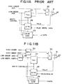
- Fig.11A shows a conventional cache data invalidating circuit
- Fig.11B shows a cache data invalidating circuit according to the embodiment of the present invention.
- the circuit shown in Fig.11A comprises a tag memory (TAG) 27, an attribute memory (ATTR) 28, a cache data memory 29, a comparator 30, and an AND gate 31.
- the address ADD is split into a high-order address and a low-order address.
- the tag memory 27, the attribute memory 28 and the cache data memory 29 are simultaneously accessed by the low-order address.
- data C is stored in an area of a main memory 35 specified by address B.
- the data C is held in a cache memory 34.
- the data in the cache memory 34 does not coincide with the data in the main memory 35.
- the cache memory 34 is accessed in order to read the data D therefrom, the data C is read out therefrom since the data C in the cache memory 34 specified by address B is still valid. That is, data D cannot be read out from the cache memory 34.
- the address RDPP in the register 12′ is read and then output to the bus.
- the data in the cache memory 34 is invalidated by using the above address (see Fig.12(b)).
- Fig.11B shows the cache data invalidating circuit which realizes the above procedure.
- the circuit shown in Fig.11B comprises multiplexers 32 and 33.
- the multiplexer 32 receives a high-order part of the address RDPP which is read out from the register 12′ and output to the common bus by the DMA controller 50.
- the multiplexer 33 receives a low-order part of the above address RDPP.
- the multiplexers 32 and 33 receive the high-order and low-order parts of the address ADD, respectively.
- the address RDPP is read out from the register 12′
- the high-order and low-order parts of the address RDPP are respectively selected by the multiplexers 32 and 33 instead of the high-order and low-order parts of the address ADD.
- the tag memory 27 and the attribute memory 29 are accessed by the selected address.
- the hit signal is output, the invalid signal is written into the attribute memory 28, so that data in the cache memory 34 can be invalidated.
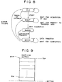
- FIG.13A A description will now be given, with reference to Figs.13A and 13B, of a circuit capable of continuously accessing data split in upper and lower part of the receiving buffer.
- a mapping is carried out so that addresses spaced apart from each other in a real memory 37 become consecutive addresses.
- An address area (address image) twice the size of the real buffer area is provided in order to avoid the separation of addresses specifying the received data.
- addresses 5C000 - 5E000 of an address image 36 are placed in addresses 5A000 - 5C000 of the real memory 37.
- Fig.13B shows an address conversion circuit which implements the above address conversion.
- An address bit AD[14:13] is converted into '01' between 5C000 - 5E000.
- a decoder (DEC) 38 detects a section in which the address conversion should be performed, and a multiplexer (MPX) 39 converts the bit value when the section is detected.
- MPX multiplexer
- a description will now be given, with reference to Fig.14, of a structure in which a plurality of receiving buffers are provided, these buffers being selectively used on the basis of the type of received data and/or the type of the accessing source.
- a plurality of sets of the registers RDP, WTP, LAR, PAR, BCMD and BRST are provided and selectively used on the basis of the message type and/or a task ID.
- Fig.14(b) is a detailed view of the structure having a plurality of receiving buffers.
- a plurality of register groups 40 - 42 relating to the respective types of, for example, messages are chained and further connected to a decoder (DEC) 44.
- a register 43 which is connected to the decoder 44, holds data showing a desired type of message. The above data is written into the register 43 by, for example, the CPU 3 (Fig.1).
- the decoder 44 decodes the data in the register 43, and selects one of the register groups 40 - 42.
- Each of the register groups 40 - 42 is assigned a plurality of addresses in order to selectively read out the data in the registers RDP, WTP, LAR, PAR, BCMD and BRST.
- the present invention has the following advantages. First, it becomes possible to omit a series of processes executed by the CPU after data arrives at the processor. Hence, it becomes possible to reduce the setup time after data is received and reduce the load of the CPU. Next, the pointers associated with the receiving buffer is automatically updated by hardware. Hence, it becomes possible to eliminate the problems arising from use of software. In addition since the data read operation can be jumped, data can be efficiently read at a high speed. Also, information showing that there is no data in the receiving buffer can be obtained by referring to the information in the registers for managing the receiving buffer. Hence, data can be efficiently read out from the receiving buffer.
- the page address is managed in the form of logical address and real address.
Landscapes
- Engineering & Computer Science (AREA)
- Computer Networks & Wireless Communication (AREA)
- Signal Processing (AREA)
- Theoretical Computer Science (AREA)
- Physics & Mathematics (AREA)
- General Engineering & Computer Science (AREA)
- General Physics & Mathematics (AREA)
- Information Transfer Systems (AREA)
- Memory System Of A Hierarchy Structure (AREA)
- Communication Control (AREA)
Applications Claiming Priority (2)
| Application Number | Priority Date | Filing Date | Title |
|---|---|---|---|
| JP7314691A JP2703417B2 (ja) | 1991-04-05 | 1991-04-05 | 受信バッファ |
| JP73146/91 | 1991-04-05 |
Publications (3)
| Publication Number | Publication Date |
|---|---|
| EP0507571A2 true EP0507571A2 (de) | 1992-10-07 |
| EP0507571A3 EP0507571A3 (en) | 1993-10-20 |
| EP0507571B1 EP0507571B1 (de) | 1998-09-23 |
Family
ID=13509769
Family Applications (1)
| Application Number | Title | Priority Date | Filing Date |
|---|---|---|---|
| EP19920302872 Expired - Lifetime EP0507571B1 (de) | 1991-04-05 | 1992-04-01 | Empfangspuffersteuerungssystem |
Country Status (5)
| Country | Link |
|---|---|
| US (1) | US5765187A (de) |
| EP (1) | EP0507571B1 (de) |
| JP (1) | JP2703417B2 (de) |
| AU (1) | AU637543B2 (de) |
| DE (1) | DE69227061T2 (de) |
Cited By (31)
| Publication number | Priority date | Publication date | Assignee | Title |
|---|---|---|---|---|
| EP0735476A1 (de) * | 1995-03-31 | 1996-10-02 | Sun Microsystems, Inc. | Verfahren und Vorrichtung zur Datenflusssteuerung in einem paketvermittelten Computersystem |
| WO1996037873A1 (en) * | 1995-05-26 | 1996-11-28 | National Semiconductor Corporation | Display controller capable of accessing graphics data from a shared system memory |
| US5634068A (en) * | 1995-03-31 | 1997-05-27 | Sun Microsystems, Inc. | Packet switched cache coherent multiprocessor system |
| US5655100A (en) * | 1995-03-31 | 1997-08-05 | Sun Microsystems, Inc. | Transaction activation processor for controlling memory transaction execution in a packet switched cache coherent multiprocessor system |
| US5657472A (en) * | 1995-03-31 | 1997-08-12 | Sun Microsystems, Inc. | Memory transaction execution system and method for multiprocessor system having independent parallel transaction queues associated with each processor |
| US5684977A (en) * | 1995-03-31 | 1997-11-04 | Sun Microsystems, Inc. | Writeback cancellation processing system for use in a packet switched cache coherent multiprocessor system |
| US5689713A (en) * | 1995-03-31 | 1997-11-18 | Sun Microsystems, Inc. | Method and apparatus for interrupt communication in a packet-switched computer system |
| US5706463A (en) * | 1995-03-31 | 1998-01-06 | Sun Microsystems, Inc. | Cache coherent computer system that minimizes invalidation and copyback operations |
| US5710891A (en) * | 1995-03-31 | 1998-01-20 | Sun Microsystems, Inc. | Pipelined distributed bus arbitration system |
| US5737755A (en) * | 1995-03-31 | 1998-04-07 | Sun Microsystems, Inc. | System level mechanism for invalidating data stored in the external cache of a processor in a computer system |
| EP0859311A1 (de) * | 1997-02-18 | 1998-08-19 | Lsi Logic Corporation | FIFO Datenpuffersystem |
| EP0864967A1 (de) * | 1997-03-10 | 1998-09-16 | International Business Machines Corporation | Bestimmung der sequentiellen Priorität in einem Ringpuffer |
| US5821910A (en) * | 1995-05-26 | 1998-10-13 | National Semiconductor Corporation | Clock generation circuit for a display controller having a fine tuneable frame rate |
| US5893165A (en) * | 1996-07-01 | 1999-04-06 | Sun Microsystems, Inc. | System and method for parallel execution of memory transactions using multiple memory models, including SSO, TSO, PSO and RMO |
| US5900886A (en) * | 1995-05-26 | 1999-05-04 | National Semiconductor Corporation | Display controller capable of accessing an external memory for gray scale modulation data |
| US6101565A (en) * | 1996-07-01 | 2000-08-08 | Sun Microsystems, Inc. | System for multisized bus coupling in a packet-switched computer system |
| GB2366935A (en) * | 2000-09-15 | 2002-03-20 | Mitel Corp | Managing buffers in a SAR |
| FR2817364A1 (fr) * | 2000-11-29 | 2002-05-31 | Thomson Multimedia Sa | Procede de detection de l'effacement d'une donnee dans une memoire geree circulairement, et dispositif pour la mise en oeuvre du procede |
| WO2004092945A3 (en) * | 2003-04-16 | 2005-01-20 | Koninkl Philips Electronics Nv | Data processing in which concurrently executed processes communicate via a fifo buffer |
| US6992957B2 (en) | 1999-12-27 | 2006-01-31 | Sanyo Electric Co., Ltd. | Controller of data recorder |
| US7042813B2 (en) * | 2002-05-13 | 2006-05-09 | Texas Instruments Incorporated | Shock protection for compressed audio on a CD player |
| US7099246B2 (en) | 2001-01-31 | 2006-08-29 | Sanyo Electric Co., Ltd. | Method and apparatus for recording data on an optical disc with restarting writing of data after data recording interruption |
| US7106675B1 (en) | 1999-11-22 | 2006-09-12 | Sanyo Electric Co., Ltd. | Data recorder |
| US7120710B2 (en) | 1999-11-22 | 2006-10-10 | Sanyo Electric Co., Ltd. | Controller for data recorder |
| US7149165B2 (en) | 1999-12-27 | 2006-12-12 | Sanyo Electric Co., Ltd. | Controller for data recorder |
| US7149167B2 (en) | 1999-12-27 | 2006-12-12 | Sanyo Electric Co., Ltd. | Data recorder |
| US7167427B1 (en) | 1999-11-22 | 2007-01-23 | Sanyo Electric Co., Ltd. | Data recorder |
| US7196987B1 (en) | 1999-11-22 | 2007-03-27 | Sanyo Electric Co., Ltd. | Controller for data recorder |
| EP1603027A3 (de) * | 1998-09-29 | 2007-05-02 | Seiko Epson Corporation | Seitendrucker und Seitendrucksystem |
| CN101526912A (zh) * | 2008-03-04 | 2009-09-09 | 英业达股份有限公司 | 内存干扰测试的系统与方法 |
| US20120176644A1 (en) * | 2011-01-06 | 2012-07-12 | Seiko Epson Corporation | Recording System, Recording Control Device, and Control Method |
Families Citing this family (38)
| Publication number | Priority date | Publication date | Assignee | Title |
|---|---|---|---|---|
| US5617088A (en) * | 1994-01-26 | 1997-04-01 | Sony Corporation | Sampling frequency converting device and memory address control device |
| DE19650993A1 (de) * | 1996-11-26 | 1998-05-28 | Francotyp Postalia Gmbh | Anordnung und Verfahren zur Verbesserung der Datensicherheit mittels Ringpuffer |
| JPH10207766A (ja) * | 1997-01-16 | 1998-08-07 | Nec Ic Microcomput Syst Ltd | 画像生成装置 |
| DE69837123T2 (de) * | 1997-04-02 | 2007-11-29 | Matsushita Electric Industrial Co., Ltd., Kadoma | Hochgeschwindigkeits-Daten-Ein/Ausgangsgerät zur Übertragung der Daten in den internen Speicher, Behandlungsausführung auf den Daten und Ausgabe der Daten |
| US5978868A (en) * | 1997-08-28 | 1999-11-02 | Cypress Semiconductor Corp. | System for generating buffer status flags by comparing read and write pointers and determining direction of progression of read pointer with respect to write pointer |
| US6092128A (en) * | 1997-08-28 | 2000-07-18 | Cypress Semiconductor Corp. | Ethernet repeater that couples an input data stream to multiple output data streams of differing rates and provides access to a shared bus by a number of inputs and outputs |
| US6148386A (en) * | 1998-03-19 | 2000-11-14 | Lucent Technologies Inc | Address generator circuity for a circular buffer |
| EP0965980A1 (de) * | 1998-06-19 | 1999-12-22 | Deutsche Thomson-Brandt Gmbh | Vorichtung zur Verstärkung und Konvertierung von Stromsignalen in Spannungssignale |
| JP3163064B2 (ja) * | 1998-07-22 | 2001-05-08 | 三洋電機株式会社 | ディスク記録装置 |
| US6363438B1 (en) * | 1999-02-03 | 2002-03-26 | Sun Microsystems, Inc. | Method of controlling DMA command buffer for holding sequence of DMA commands with head and tail pointers |
| GB2350533B (en) | 1999-05-28 | 2001-07-04 | Mitel Corp | Method to control data reception buffers for packetized voice channels |
| US6408409B1 (en) * | 1999-11-15 | 2002-06-18 | Sun Microsystems, Inc. | Method and apparatus for ring buffer flow error detection |
| US6480912B1 (en) | 2000-07-21 | 2002-11-12 | Stmicroelectronics, Inc. | Method and apparatus for determining the number of empty memory locations in a FIFO memory device |
| US6952739B2 (en) * | 2000-08-03 | 2005-10-04 | International Business Machines Corporation | Method and device for parameter independent buffer underrun prevention |
| JP3801088B2 (ja) * | 2002-04-19 | 2006-07-26 | 株式会社デンソー | 車両用通信装置 |
| US7697946B2 (en) * | 2002-06-04 | 2010-04-13 | Forster Ian J | Reflective communication using radio-frequency devices |
| WO2004004251A1 (ja) * | 2002-07-01 | 2004-01-08 | Ipsquare Inc. | 半導体回路デバイス、パケット処理方法、管理システム、管理方法、及びパケット処理方法 |
| US20050262314A1 (en) * | 2004-05-21 | 2005-11-24 | Oh Yong S | System and method for circular buffer |
| CN1957329B (zh) * | 2004-05-27 | 2010-05-12 | Nxp股份有限公司 | 信号处理装置 |
| US20060075184A1 (en) * | 2004-10-01 | 2006-04-06 | Jen-Ying Chen | Synchronous\asynchronous memory device with single port memory unit |
| TWI237806B (en) * | 2004-11-03 | 2005-08-11 | Sunplus Technology Co Ltd | Audio decoding system with ring buffer and method thereof |
| US7350040B2 (en) * | 2005-03-03 | 2008-03-25 | Microsoft Corporation | Method and system for securing metadata to detect unauthorized access |
| WO2007054757A1 (en) * | 2005-11-09 | 2007-05-18 | Freescale Semiconductor, Inc. | A method for managing under-run and a device having under-run management capabilities |
| US7886090B2 (en) * | 2006-01-04 | 2011-02-08 | Freescale Semiconductor, Inc. | Method for managing under-runs and a device having under-run management capabilities |
| US20080148399A1 (en) * | 2006-10-18 | 2008-06-19 | Microsoft Corporation | Protection against stack buffer overrun exploitation |
| KR101344475B1 (ko) * | 2007-01-05 | 2013-12-24 | 삼성전자주식회사 | 메모리 관리방법 및 장치 |
| JP2008293484A (ja) * | 2007-04-27 | 2008-12-04 | Panasonic Corp | バッファメモリ共有装置 |
| JP4854598B2 (ja) * | 2007-05-31 | 2012-01-18 | 三菱電機株式会社 | データ転送制御装置 |
| EP2045973A1 (de) * | 2007-10-02 | 2009-04-08 | Deutsche Thomson OHG | Speicherpuffersystem und Verfahren zum Betreiben eines Speicherpuffersystems für schnellen Datenaustausch |
| US8291136B2 (en) * | 2009-12-02 | 2012-10-16 | International Business Machines Corporation | Ring buffer |
| GB2482303A (en) * | 2010-07-28 | 2012-02-01 | Gnodal Ltd | Modifying read patterns for a FIFO between clock domains |
| DE112013001213T5 (de) | 2012-02-29 | 2014-12-04 | Mitsubishi Electric Corporation | Datentransfereinrichtung, Datentransferverfahren und Datentransferprogramm |
| JP5598493B2 (ja) | 2012-03-30 | 2014-10-01 | 富士通株式会社 | 情報処理装置、演算装置および情報転送方法 |
| US20140068139A1 (en) * | 2012-08-29 | 2014-03-06 | Advanced Micro Devices, Inc. | Data transfer system and method |
| US10516740B2 (en) * | 2014-05-30 | 2019-12-24 | Apple Inc. | Dynamic transport switching in inter-device communication |
| JP6334376B2 (ja) * | 2014-12-02 | 2018-05-30 | 株式会社東芝 | 通信装置及びディスクリプタオーバーフロー検出方法 |
| CN110557341A (zh) * | 2018-05-31 | 2019-12-10 | 北京京东尚科信息技术有限公司 | 数据限流的方法和装置 |
| CN111372038B (zh) * | 2018-12-26 | 2021-06-18 | 厦门星宸科技有限公司 | 多串流影像处理装置及方法 |
Family Cites Families (28)
| Publication number | Priority date | Publication date | Assignee | Title |
|---|---|---|---|---|
| GB1441816A (en) * | 1973-07-18 | 1976-07-07 | Int Computers Ltd | Electronic digital data processing systems |
| DE2714106C3 (de) * | 1977-03-30 | 1982-01-14 | Telefonbau Und Normalzeit Gmbh, 6000 Frankfurt | Verfahren zum Zwischenspeichern von Informationen in einem FIFO-Speicher |
| US4175287A (en) * | 1978-01-23 | 1979-11-20 | Rockwell International Corporation | Elastic store slip control circuit apparatus and method for preventing overlapping sequential read and write operations |
| US4504902A (en) * | 1982-03-25 | 1985-03-12 | At&T Bell Laboratories | Cache arrangement for direct memory access block transfer |
| JPS59112327A (ja) * | 1982-12-20 | 1984-06-28 | Hitachi Ltd | リングバツフア制御方式 |
| JPS60178570A (ja) * | 1984-02-24 | 1985-09-12 | Nec Corp | デ−タ受信器 |
| US4648033A (en) * | 1984-09-07 | 1987-03-03 | International Business Machines Corporation | Look-aside buffer LRU marker controller |
| US4692894A (en) * | 1984-12-18 | 1987-09-08 | Advanced Micro Devices, Inc. | Overflow/Underflow detection for elastic buffer |
| US4704697A (en) * | 1985-06-17 | 1987-11-03 | Counterpoint Computers | Multiple station video memory |
| JPS62184561A (ja) * | 1986-02-07 | 1987-08-12 | Matsushita Electric Ind Co Ltd | 入出力バツフア制御装置 |
| JPS62184560A (ja) * | 1986-02-07 | 1987-08-12 | Matsushita Electric Ind Co Ltd | 入出力バツフア制御装置 |
| US4949301A (en) * | 1986-03-06 | 1990-08-14 | Advanced Micro Devices, Inc. | Improved pointer FIFO controller for converting a standard RAM into a simulated dual FIFO by controlling the RAM's address inputs |
| US5133062A (en) * | 1986-03-06 | 1992-07-21 | Advanced Micro Devices, Inc. | RAM buffer controller for providing simulated first-in-first-out (FIFO) buffers in a random access memory |
| JPS62208153A (ja) * | 1986-03-08 | 1987-09-12 | Nec Corp | 入出力バツフア装置 |
| GB2190220A (en) * | 1986-05-09 | 1987-11-11 | Int Computers Ltd | Multi-level storage system |
| JPS63291134A (ja) * | 1987-05-22 | 1988-11-29 | Toshiba Corp | 論理集積回路 |
| JPH01143080A (ja) * | 1987-11-30 | 1989-06-05 | Sony Corp | 記録装置 |
| US4980816A (en) * | 1987-12-18 | 1990-12-25 | Nec Corporation | Translation look-aside buffer control system with multiple prioritized buffers |
| US4945548A (en) * | 1988-04-28 | 1990-07-31 | Digital Equipment Corporation | Method and apparatus for detecting impending overflow and/or underrun of elasticity buffer |
| JPH0650486B2 (ja) * | 1988-05-24 | 1994-06-29 | 日本電気株式会社 | データチェイン処理方式 |
| JPH0223439A (ja) * | 1988-07-13 | 1990-01-25 | Mitsubishi Electric Corp | データ処理装置 |
| JP2556558B2 (ja) * | 1988-09-09 | 1996-11-20 | 沖電気工業株式会社 | ファーストイン・ファーストアウトメモリ |
| JP2523814B2 (ja) * | 1988-09-20 | 1996-08-14 | 富士通株式会社 | ム―ブアウト・システム |
| EP0369920A3 (de) * | 1988-11-18 | 1992-01-15 | Rolm Company | Verschachtelung von Ringpuffern |
| US4995041A (en) * | 1989-02-03 | 1991-02-19 | Digital Equipment Corporation | Write back buffer with error correcting capabilities |
| JPH04506425A (ja) * | 1989-06-30 | 1992-11-05 | ポケット コンピューター コーポレイション | 計算機システムにおける情報管理方法及び装置 |
| JPH0337870A (ja) * | 1989-07-05 | 1991-02-19 | Matsushita Electric Ind Co Ltd | 書き込み制御回路 |
| GB2247546B (en) * | 1990-08-31 | 1995-03-01 | Sun Microsystems Inc | Method and apparatus for predictive caching |
-
1991
- 1991-04-05 JP JP7314691A patent/JP2703417B2/ja not_active Expired - Lifetime
-
1992
- 1992-04-01 DE DE69227061T patent/DE69227061T2/de not_active Expired - Lifetime
- 1992-04-01 EP EP19920302872 patent/EP0507571B1/de not_active Expired - Lifetime
- 1992-04-01 AU AU13967/92A patent/AU637543B2/en not_active Ceased
-
1997
- 1997-04-22 US US08/844,852 patent/US5765187A/en not_active Expired - Lifetime
Cited By (38)
| Publication number | Priority date | Publication date | Assignee | Title |
|---|---|---|---|---|
| US5689713A (en) * | 1995-03-31 | 1997-11-18 | Sun Microsystems, Inc. | Method and apparatus for interrupt communication in a packet-switched computer system |
| EP0735476A1 (de) * | 1995-03-31 | 1996-10-02 | Sun Microsystems, Inc. | Verfahren und Vorrichtung zur Datenflusssteuerung in einem paketvermittelten Computersystem |
| US5634068A (en) * | 1995-03-31 | 1997-05-27 | Sun Microsystems, Inc. | Packet switched cache coherent multiprocessor system |
| US5655100A (en) * | 1995-03-31 | 1997-08-05 | Sun Microsystems, Inc. | Transaction activation processor for controlling memory transaction execution in a packet switched cache coherent multiprocessor system |
| US5657472A (en) * | 1995-03-31 | 1997-08-12 | Sun Microsystems, Inc. | Memory transaction execution system and method for multiprocessor system having independent parallel transaction queues associated with each processor |
| US5684977A (en) * | 1995-03-31 | 1997-11-04 | Sun Microsystems, Inc. | Writeback cancellation processing system for use in a packet switched cache coherent multiprocessor system |
| US5710891A (en) * | 1995-03-31 | 1998-01-20 | Sun Microsystems, Inc. | Pipelined distributed bus arbitration system |
| US5706463A (en) * | 1995-03-31 | 1998-01-06 | Sun Microsystems, Inc. | Cache coherent computer system that minimizes invalidation and copyback operations |
| US5907485A (en) * | 1995-03-31 | 1999-05-25 | Sun Microsystems, Inc. | Method and apparatus for flow control in packet-switched computer system |
| US5737755A (en) * | 1995-03-31 | 1998-04-07 | Sun Microsystems, Inc. | System level mechanism for invalidating data stored in the external cache of a processor in a computer system |
| US5892957A (en) * | 1995-03-31 | 1999-04-06 | Sun Microsystems, Inc. | Method and apparatus for interrupt communication in packet-switched microprocessor-based computer system |
| WO1996037873A1 (en) * | 1995-05-26 | 1996-11-28 | National Semiconductor Corporation | Display controller capable of accessing graphics data from a shared system memory |
| US5821910A (en) * | 1995-05-26 | 1998-10-13 | National Semiconductor Corporation | Clock generation circuit for a display controller having a fine tuneable frame rate |
| US5900886A (en) * | 1995-05-26 | 1999-05-04 | National Semiconductor Corporation | Display controller capable of accessing an external memory for gray scale modulation data |
| US6101565A (en) * | 1996-07-01 | 2000-08-08 | Sun Microsystems, Inc. | System for multisized bus coupling in a packet-switched computer system |
| US5893165A (en) * | 1996-07-01 | 1999-04-06 | Sun Microsystems, Inc. | System and method for parallel execution of memory transactions using multiple memory models, including SSO, TSO, PSO and RMO |
| EP0859311A1 (de) * | 1997-02-18 | 1998-08-19 | Lsi Logic Corporation | FIFO Datenpuffersystem |
| US6101329A (en) * | 1997-02-18 | 2000-08-08 | Lsi Logic Corporation | System for comparing counter blocks and flag registers to determine whether FIFO buffer can send or receive data |
| EP0864967A1 (de) * | 1997-03-10 | 1998-09-16 | International Business Machines Corporation | Bestimmung der sequentiellen Priorität in einem Ringpuffer |
| US5923900A (en) * | 1997-03-10 | 1999-07-13 | International Business Machines Corporation | Circular buffer with n sequential real and virtual entry positions for selectively inhibiting n adjacent entry positions including the virtual entry positions |
| EP1603027A3 (de) * | 1998-09-29 | 2007-05-02 | Seiko Epson Corporation | Seitendrucker und Seitendrucksystem |
| US7236436B2 (en) | 1999-11-22 | 2007-06-26 | Sanyo Electric Co., Ltd. | Controller for data recorder |
| US7196987B1 (en) | 1999-11-22 | 2007-03-27 | Sanyo Electric Co., Ltd. | Controller for data recorder |
| US7167427B1 (en) | 1999-11-22 | 2007-01-23 | Sanyo Electric Co., Ltd. | Data recorder |
| US7106675B1 (en) | 1999-11-22 | 2006-09-12 | Sanyo Electric Co., Ltd. | Data recorder |
| US7120710B2 (en) | 1999-11-22 | 2006-10-10 | Sanyo Electric Co., Ltd. | Controller for data recorder |
| US7149165B2 (en) | 1999-12-27 | 2006-12-12 | Sanyo Electric Co., Ltd. | Controller for data recorder |
| US6992957B2 (en) | 1999-12-27 | 2006-01-31 | Sanyo Electric Co., Ltd. | Controller of data recorder |
| US7149167B2 (en) | 1999-12-27 | 2006-12-12 | Sanyo Electric Co., Ltd. | Data recorder |
| GB2366935A (en) * | 2000-09-15 | 2002-03-20 | Mitel Corp | Managing buffers in a SAR |
| GB2366935B (en) * | 2000-09-15 | 2004-01-07 | Mitel Corp | Method of checking for and recovering from underruns and overrun slips when writing to circular buffers in dynamic bandwidth circuit emulation services |
| FR2817364A1 (fr) * | 2000-11-29 | 2002-05-31 | Thomson Multimedia Sa | Procede de detection de l'effacement d'une donnee dans une memoire geree circulairement, et dispositif pour la mise en oeuvre du procede |
| US7099246B2 (en) | 2001-01-31 | 2006-08-29 | Sanyo Electric Co., Ltd. | Method and apparatus for recording data on an optical disc with restarting writing of data after data recording interruption |
| US7042813B2 (en) * | 2002-05-13 | 2006-05-09 | Texas Instruments Incorporated | Shock protection for compressed audio on a CD player |
| WO2004092945A3 (en) * | 2003-04-16 | 2005-01-20 | Koninkl Philips Electronics Nv | Data processing in which concurrently executed processes communicate via a fifo buffer |
| CN101526912A (zh) * | 2008-03-04 | 2009-09-09 | 英业达股份有限公司 | 内存干扰测试的系统与方法 |
| US20120176644A1 (en) * | 2011-01-06 | 2012-07-12 | Seiko Epson Corporation | Recording System, Recording Control Device, and Control Method |
| US8699070B2 (en) * | 2011-01-06 | 2014-04-15 | Seiko Epson Corporation | Control method for replacing data rendering blocks of white space with paper feed commands |
Also Published As
| Publication number | Publication date |
|---|---|
| DE69227061D1 (de) | 1998-10-29 |
| US5765187A (en) | 1998-06-09 |
| AU637543B2 (en) | 1993-05-27 |
| JP2703417B2 (ja) | 1998-01-26 |
| EP0507571A3 (en) | 1993-10-20 |
| EP0507571B1 (de) | 1998-09-23 |
| JPH04308956A (ja) | 1992-10-30 |
| DE69227061T2 (de) | 1999-02-11 |
| AU1396792A (en) | 1992-10-15 |
Similar Documents
| Publication | Publication Date | Title |
|---|---|---|
| EP0507571B1 (de) | Empfangspuffersteuerungssystem | |
| KR920004402B1 (ko) | 디지탈 데이타 프로세서용 버스 인터페이스 회로 | |
| JP2599563B2 (ja) | アービタ回路を有するデータ・プロセッサ・システム | |
| US5283883A (en) | Method and direct memory access controller for asynchronously reading/writing data from/to a memory with improved throughput | |
| KR100766732B1 (ko) | 고속의 낮은 오버헤드의 콘텍스트 전환을 실행하는 디바이스 및 방법 | |
| US5497501A (en) | DMA controller using a predetermined number of transfers per request | |
| EP0351955B1 (de) | Mehrprozessoranordnungen mit kreuzweise abgefragten Schreib-in-Cachespeichern | |
| JPS6327738B2 (de) | ||
| KR19990045059A (ko) | 캐시 메모리 시스템 | |
| JP2001117859A (ja) | バス制御装置 | |
| JPH10154102A (ja) | 多重階層のキャッシュ・メモリを有する情報処理システムにおけるデータ・コヒーレンシを強化する装置および方法 | |
| EP0427023B1 (de) | Datenübertragungssteuervorrichtung für Parallelverarbeitungssysteme | |
| US4658356A (en) | Control system for updating a change bit | |
| JPH0532775B2 (de) | ||
| JPH1083349A (ja) | キャッシュ・メモリ・バンク制御装置 | |
| US5418744A (en) | Data transfer apparatus | |
| JP2002024007A (ja) | プロセッサシステム | |
| JPH03147157A (ja) | 情報処理装置 | |
| JP3162459B2 (ja) | データ処理装置 | |
| US5440696A (en) | Data processing device for reducing the number of internal bus lines | |
| JPH04195576A (ja) | キャッシュメモリ方式 | |
| JP3039391B2 (ja) | メモリシステム | |
| JPH09146839A (ja) | キャッシュメモリ制御装置 | |
| JP2980163B2 (ja) | データ転送方式 | |
| JPH0756844A (ja) | システムメモリを有するバスをベースにしたコンピュータシステムに使用するためのマスタバスマスタおよびバスをベースにしたコンピュータシステム |
Legal Events
| Date | Code | Title | Description |
|---|---|---|---|
| PUAI | Public reference made under article 153(3) epc to a published international application that has entered the european phase |
Free format text: ORIGINAL CODE: 0009012 |
|
| AK | Designated contracting states |
Kind code of ref document: A2 Designated state(s): DE FR GB |
|
| PUAL | Search report despatched |
Free format text: ORIGINAL CODE: 0009013 |
|
| AK | Designated contracting states |
Kind code of ref document: A3 Designated state(s): DE FR GB |
|
| 17P | Request for examination filed |
Effective date: 19940414 |
|
| 17Q | First examination report despatched |
Effective date: 19970425 |
|
| GRAG | Despatch of communication of intention to grant |
Free format text: ORIGINAL CODE: EPIDOS AGRA |
|
| GRAG | Despatch of communication of intention to grant |
Free format text: ORIGINAL CODE: EPIDOS AGRA |
|
| GRAH | Despatch of communication of intention to grant a patent |
Free format text: ORIGINAL CODE: EPIDOS IGRA |
|
| RBV | Designated contracting states (corrected) |
Designated state(s): DE GB |
|
| GRAH | Despatch of communication of intention to grant a patent |
Free format text: ORIGINAL CODE: EPIDOS IGRA |
|
| GRAA | (expected) grant |
Free format text: ORIGINAL CODE: 0009210 |
|
| AK | Designated contracting states |
Kind code of ref document: B1 Designated state(s): DE GB |
|
| REF | Corresponds to: |
Ref document number: 69227061 Country of ref document: DE Date of ref document: 19981029 |
|
| PLBE | No opposition filed within time limit |
Free format text: ORIGINAL CODE: 0009261 |
|
| STAA | Information on the status of an ep patent application or granted ep patent |
Free format text: STATUS: NO OPPOSITION FILED WITHIN TIME LIMIT |
|
| 26N | No opposition filed | ||
| REG | Reference to a national code |
Ref country code: GB Ref legal event code: IF02 |
|
| PGFP | Annual fee paid to national office [announced via postgrant information from national office to epo] |
Ref country code: GB Payment date: 20110330 Year of fee payment: 20 Ref country code: DE Payment date: 20110330 Year of fee payment: 20 |
|
| REG | Reference to a national code |
Ref country code: DE Ref legal event code: R071 Ref document number: 69227061 Country of ref document: DE |
|
| REG | Reference to a national code |
Ref country code: DE Ref legal event code: R071 Ref document number: 69227061 Country of ref document: DE |
|
| REG | Reference to a national code |
Ref country code: GB Ref legal event code: PE20 Expiry date: 20120331 |
|
| PG25 | Lapsed in a contracting state [announced via postgrant information from national office to epo] |
Ref country code: GB Free format text: LAPSE BECAUSE OF EXPIRATION OF PROTECTION Effective date: 20120331 |
|
| PG25 | Lapsed in a contracting state [announced via postgrant information from national office to epo] |
Ref country code: DE Free format text: LAPSE BECAUSE OF EXPIRATION OF PROTECTION Effective date: 20120402 |