US6148386A - Address generator circuity for a circular buffer - Google Patents
Address generator circuity for a circular buffer Download PDFInfo
- Publication number
- US6148386A US6148386A US09/044,529 US4452998A US6148386A US 6148386 A US6148386 A US 6148386A US 4452998 A US4452998 A US 4452998A US 6148386 A US6148386 A US 6148386A
- Authority
- US
- United States
- Prior art keywords
- register
- data
- output port
- data output
- address
- Prior art date
- Legal status (The legal status is an assumption and is not a legal conclusion. Google has not performed a legal analysis and makes no representation as to the accuracy of the status listed.)
- Expired - Fee Related
Links
Images


Classifications
-
- G—PHYSICS
- G06—COMPUTING; CALCULATING OR COUNTING
- G06F—ELECTRIC DIGITAL DATA PROCESSING
- G06F5/00—Methods or arrangements for data conversion without changing the order or content of the data handled
- G06F5/06—Methods or arrangements for data conversion without changing the order or content of the data handled for changing the speed of data flow, i.e. speed regularising or timing, e.g. delay lines, FIFO buffers; over- or underrun control therefor
- G06F5/10—Methods or arrangements for data conversion without changing the order or content of the data handled for changing the speed of data flow, i.e. speed regularising or timing, e.g. delay lines, FIFO buffers; over- or underrun control therefor having a sequence of storage locations each being individually accessible for both enqueue and dequeue operations, e.g. using random access memory
-
- G—PHYSICS
- G06—COMPUTING; CALCULATING OR COUNTING
- G06F—ELECTRIC DIGITAL DATA PROCESSING
- G06F2205/00—Indexing scheme relating to group G06F5/00; Methods or arrangements for data conversion without changing the order or content of the data handled
- G06F2205/10—Indexing scheme relating to groups G06F5/10 - G06F5/14
- G06F2205/106—Details of pointers, i.e. structure of the address generators
Definitions
- This application includes a microfiche appendix having 1 sheet of microfiche and a total of 19 frames.
- This invention relates to improved methods and apparatus for providing computer memory addresses particularly addresses for use in accessing circular buffers in memory devices.
- FIG. 9 At least two feedback circuits are shown for providing the address generation.
- One feedback circuit comprises the address pointer register 24 and a second feedback circuit comprises an advanced address pointer register 94.
- the circuit has been shown in the present application as FIG. 1. These feedback circuits share an adder 40.
- the feedback circuit with the address pointer register 24 has a phase delay latch 96 but the feedback circuit with the advanced address pointer register 94 does not have a phase delay latch.
- the technique disclosed in Holmquist has very stringent timing requirements. These timing requirements may not be met and may cause erroneous addresses to be generated. There is a need for better techniques for generating addresses for accessing circular memory buffers.
- the present invention in one embodiment provides an improved method and apparatus for providing addresses for accessing computer memory, particularly circular buffer memory.
- the present invention improves upon devices such as disclosed in patent application Ser. No. 08/932,977, filed on Sep. 18, 1997 to Holmqvist, et al. incorporated by reference herein.
- the present invention in one embodiment, comprises first and second feedback circuits where both circuits include their own separate, different adders, displacement registers, and phase delay registers.
- both circuits include their own separate, different adders, displacement registers, and phase delay registers.
- Such components along with a different method of operation allow the present invention in one or more embodiment to provide better timing constraints.
- the present invention in some embodiments provides an apparatus comprised of a first feedback circuit, a second feedback circuit, a beginning address register, an ending address register, a comparator circuit, and a control circuit.
- the beginning and ending address registers preferably include the beginning and ending addresses respectively of a circular memory buffer.
- the first feedback circuit is preferably comprised of a first register, a first phase delay register, a first adder, a first displacement register, and a first multiplexer.
- the first register has a data input port connected to a data output port of the first adder, and a data output port connected to a data input port of the first phase delay register.
- the data output port of the first adder is connected to the data input port of the first register through a first data input port of a first multiplexer and a data output port of the first multiplexer.
- the first phase delay register also has a data output port connected to the first data input port of the first adder.
- the first adder has a second data input port connected to a data output port of the first displacement register.
- the control circuit preferably provides output signals or output data to control supplying of the data input or input signals to the first register, the status of the first multiplexer, and the value contained in the first displacement register.
- the second feedback circuit is preferably comprised of a second register, a second phase delay register, a second adder, and a second displacement register.
- the second register has a data input port connected to a data output port of the second adder, and a data output port connected to a data input port of the second phase delay register.
- the second phase delay register also has a data output port connected to the first data input port of the second adder.
- the second adder also has a second data input port connected to a data output port of the second displacement register.
- the control circuit preferably provides output signals to control supplying of the data input port to the second register and the value contained in the first displacement register.
- control circuit based at least partially on the data output of the first register causes data at the data output port of the first register of the first feedback circuit to be supplied to an address bus during one or more first register cycles and data at the data output port of the second register of the second feedback circuit to be supplied to the address bus during one or more second register cycles.
- FIG. 1 shows an address generator circuit from a prior patent application
- FIG. 2A shows an apparatus in accordance with an embodiment the present invention
- FIG. 2B shows a control circuit in accordance with an embodiment of the present invention with output and input signals
- FIGS. 3A-B, 4A-B, 5A-B, 6A-B, 7A-B, and 8A-B show signal and/or data timing diagrams for cases 1, 2, 3/4, 5/6, 7, and 8 in accordance with the present invention
- FIG. 1 shows a technique which has been disclosed in a patent application to Holmqvist. Unlike an embodiment of the invention, the FIG. 1 circuit includes only a single adder 40, a single displacement register 36, and generally operates in a manner which is different from embodiments of the present invention.
- the misaligned fetch is executed in two cycles.
- the first memory access which is a single-word access, retrieves a first word and assembles it for transmission on data bus 90.
- the current address pointer 22 is placed on address bus 34 by way of bus 26, and displacement 36 is added to the current address pointer 22 to produce an updated address pointer.
- the updated address pointer is provided both to address pointer latch 24 and misalign address latch 94.
- the second memory access is a double-word fetch, even though only a single word is necessary to meet the requirements of the misaligned double-word memory access being executed.
- the two words fetched are split with the word having a higher address stored in a temporary register or data buffer 92 for potential use in a subsequent misaligned memory access.
- the advanced address 98 stored in misaligned address latch 94 is placed on address bus 34 by way of bus 108 with the least significant bit forced to be zero by AND gate 100.
- AND gate 100 receives a first input bit zero of the advanced address 98 and receives as a second input over bus 104 a signal from control circuit 52' that is a logic low at the input of AND gate 100. In this manner the output of AND gate 100 is assured to be a logic zero.
- the advanced address 98 with the least significant bit forced to be zero provides the memory address that is placed on bus 34 and from which data is retrieved.
- Misalignment is detected by the indicator of address pointer 22 which is the least significant bit for double-word memory accesses.
- the word having a lower address is assembled with the data read from the previous memory access and transmitted over data bus 90.
- the updated address pointer output from adder 40 is provided not only to address pointer latch 24 over bus 44 but also to a misaligned address latch 94 where it is stored.
- Control circuit 52' provides the updated address pointer 22 to adder 40 over bus 102 as a first input and the displacement, which is 2, to adder 40 as a second input.
- Adder 40 adds the inputs to provide an advanced address 98 as an output from adder 40.
- the advanced address 98 output is provided to misalign address latch 94 where the advanced address 98 is two greater than the address pointer 24 stored in address pointer latch 22.
- the advanced address 98 stored in misaligned address latch 94 is placed on address bus 34 with the least significant bit forced to be zero by AND gate 100.
- AND gate 100 receives as a first input bit zero of the advanced address 98 and receives as a second input over bus 104 a signal from control circuit 52' that is a logic low at the input of AND gate 100. In this manner the output of AND gate 100 is assured to be a logic zero.
- the advanced address 98 with the least significant bit forced to be zero provides the memory address that is placed on bus 34 and from which data is retrieved.
- each contiguous, subsequent misaligned double-word memory access places advanced address 98 stored in misaligned address latch 94 on the address bus and provides advanced address 98 over bus 106 as an updated pointer 22 to address pointer latch 24 by way of race eliminating delayed misaligned address latch 96.
- Adder 40 receives advanced address 98 and displacement 36 as inputs and provides an output that updates advanced address pointer 98 in misaligned address latch 94 to update or maintain the advanced address pointer at two greater than the address pointer 22.
- the advanced address pointer 98 value is copied to the address pointer 22, over bus 106 by way of delayed misaligned address latch 96. Only one adder is required to update both the advanced address pointer 98 and address pointer 22 because the advanced address pointer value is shifted into address pointer latch 24 as well as being placed onto address bus 34 such that only the advanced address pointer requires an addition operation to be updated.”
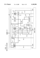
- the general purpose of the apparatus 110 shown in FIG. 2A and the control circuit 720 of FIG. 2B is to supply addresses or signals YAB on the address bus which is data output port 620c shown in FIG. 2B, for the purpose of accessing a circular memory buffer (not shown) having a certain fixed beginning address (stored in a beginning address register 320) and a certain fixed ending address (stored in an ending address register 420).
- the apparatus 110 comprises a first feedback circuit 120, a second feedback circuit 220, a beginning address register 320 and OR gate 322, an ending address register 420, a comparator circuit 520, a second multiplexer 620 and an And Gate circuit 622
- the first feedback circuit 120 includes a first register 122 (which will at times be referred to as "R0" since it holds the value of "R0" or the signal or data "R0” also known as the pointer value), a first phase delay register 124, a first adder 126, a first displacement register 128 and a first multiplexer 130.
- a data output port 122a of the first register 122 is connected to the data input port 124a of the first phase delay register 124.
- the signal YADE is located on the data output port 122a and the data input port 124a.
- the data output port 126a of the first phase delay register 124 is connected to a first data input port 126a of the first adder 126.
- the signal YA is located on the data output port 126a.
- the data output port 126b of the first displacement register 128 is connected to a second data input port 126b of the first adder 126.
- the signal YB is located on the data input port 126b.
- the data output port 130a of the first adder 126 is connected to a first data input port 130a of the first multiplexer 130.
- the signal YS is located on the first data input port 130a.
- the second data input port 130b of the first multiplexer 130 is connected to the modified data output port 320c from the beginning address register 320 after the output port 322a of the Or circuit 322.
- the signal RBB is located on the input port 130b.
- the beginning register 320 has an output port 320a which is split into output port 320b comprised of all the bits except the least significant bit, and output port 322b which is comprised of the least significant bit.
- the output port 322b is input to the OR gate 322 along with the input port 321a.
- the signal FORCLSB is located on the input port 321a.
- the single bit output port 322a from the OR gate 322 is combined with the output port 320b to form a complete output or word at input port 130b.
- the signal RBB is located on input port 130b and is the modified beginning address however it may be referred to as the beginning address for convenience.
- the second feedback circuit 220 includes a second register 222 (which at times will be referred to as "RTMP", since it holds the value of "RTMP” also known as the data or signal "RTMP”, also known as the temporary pointer register), a second phase delay register 224, a second adder 226, and a second displacement register 228.
- the data output port 222a of the second register is connected to the data input port 224b of the second phase delay register 224.
- the signal RBUS is located on the output port 222a.
- the data output port 224a of the second phase delay register 224 is connected to the second data input port 224a of the second adder 226.
- the signal YB2 is located on the second data input port 224a.
- the first data input port 228a of the second adder 226 is connected to the data output port 228a of the second displacement register 228.
- the signal YA2 is located on the output port 228a.
- the second register 222 also has a first data input port 222b which is connected to the output port 122a of the first register, and a second data input port 222c which is connected to the modified output port 320c from the beginning address register 320 and Or gate 322.
- the signal YADE is located on the data input port 222b.
- the signal REB is located on the data input port 222c.
- the data output port 222a of the second register 222 is also connected to a second data input port 520a of the comparison circuit 520.
- the first data input port 420a of the comparison circuit 520 is connected to the data output port 420a of the ending address register 420.
- the signal RE is located on the first data input port 420a.
- the data output port 122a from the first feedback circuit 120 and the data output port 222a from the second feedback circuit 220 are supplied as first and second data input ports, respectively, to the second multiplexer 620.
- the data output port 620a of the second multiplexer 620 is split into a data output port 620b of all the bits except the least significant bit and data output port 622a of the least significant bit.
- the data output port 622a is supplied as an input port to AND gate circuit 622 along with the input port 622b.
- the signal ZEROLSB is located on input port 622b.
- the output port 622c of the OR gate is combined with the output port 620b to form a complete output port 620c, which is the address bus.
- the YAB signal, or address bus signal is located on the output port 620c.
- control circuit 720 has the following input and output signals.
- RELSB Least significant bit of Ending Address contained in Ending address register 420 ("RE").
- RBLSB Least significant bit of Beginning Address contained in Beginning address register 320 ("RB").
- ROLSB Least significant bit of Address Pointer contained in first register 122 ("R0").
- EQ Output signal on output 520a of Comparison Circuit 520 which specifies whether the temporary address pointer in second register 222 ("RTMP") is equal (at times disregarding least significant bits) to the ending address in ending address register 420.
- RTMP temporary address pointer in second register 222
- Control Circuit 720 OUTPUT signals (Each signal has a value of "0" or "1" unless indicated):
- RTMP i.e. second register 222 not loaded from output signal YS2.
- RTMP (i.e. in second register 222) passes through multiplexer 620 and after modification as address output signal YAB.
- R0 (i.e. first register 122) passes through multiplexer 620 and after modification as address output signal YAB.
- the control circuit 720 in addition to the above input and output signals from and to the apparatus 110, keeps track of a variable called "STATE".
- the control circuit 720 executes a repetitive series of "STATEs” in order to implement an embodiment of the invention.
- the "STATEs” executed depend on whether the beginning address (RB) in beginning address register 320, the ending address (RE) in ending address register 420, and the pointer address (R0) in first register 122, are odd or even.
- RB beginning address
- RE ending address
- R0 pointer address
- FIGS. 3A-B, 4A-B, 5A-B, 6A-B, 7A-B, and 8A-B show the timing of output and input signals for apparatus 110 and control circuit 720, for Cases 1, 2, 3/4, 5/6, 7 and 8, respectively.
- YCLK is a clock signal which may be located on the control circuit 720.
- the first register 122 (R0) is loaded by control circuit 720 with an initial address
- the second register 222 (RTMP) is loaded by R0 value
- displacement constants YBCONST and YA2CONST are set to 2
- the first multiplexer 130 passes the input signal YS from the first adder 126 for incrementing the address
- the second multiplexer 620 passes the input signal R0 (or YADE) from R0 to the address bus YAB.
- Control circuit 720 sets these variables or signals to the following values (note the use of "i” after signals below to provide a clocked output.
- the “i” signals are pure combinational logic and are used as data to flips flops, not shown, which are triggered by the leading edge of the clock pulses CLK).
- the “i” signals are what is going to happen the next clock cycle. (The “i” variables or signals are shown in lower case as used in the computer program, attached):
- connection is used in a broad sense in this application to include inputs and outputs which are connected by wireless connections.
- the “signals” such as the signal RBUS and other signals shown in FIGS. 3A-8B, can each be termed “data” also.
- RBUS can be termed a “signal” or a piece of "data”, at the physical data output port 222a of the second register 222.
- the circuit disclosed in an embodiment of the present invention also has the following additional advantages over the FIG. 9 embodiment in Holmquist.
- pointer registers i.e. R0
- R0 pointer registers
- RE ending register
- EQ equality comparator output
- the output shown herein in FIG. 1 and labelled as "34" is determined in the current cycle by the comparator 46 output 54.
Abstract
Description
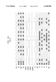
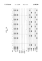
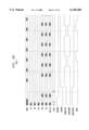
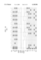
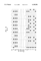
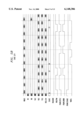
______________________________________
Table of Cases:
RB      RE       R0     Case    STATEs Executed
______________________________________
Even    Odd      Even   1       F, 0,
Even    Odd      Odd    2       F, 1, 0, 2
Even    Even     Even   3       F, 0, 3
Even    Even     Odd    4       F, 0, 3
Odd     Odd      Odd    5       F, 4, 0, 5, 6
Odd     Odd      Even   6       F, 4, 0, 5, 6
Odd     Even     Even   7       F, 0, 7
Odd     Even     Odd    8       F, 0, 8
______________________________________
(RB-even, RE-odd, R0-Even, EQU=0)
__________________________________________________________________________
Roldymi = 0:
R0 is loaded with the RBB on the leading edge of
the clock, not from output signal YM.
Rbforclsbi = 0:
rtmpldys2i = 0:
rtmpldrbbi = 0:
rtmpldyadei = 1:
RTMP (second register 222 is loaded with R0
(first register 122), from output signal YADE
just after R0 has been changed to 10, on
leading edge of clock.
ybconsti = 1:
YBCONST displacement takes on a value of 2.
ya2consti = 1:
YACONST displacement takes on a value of 2.
ymseli = 0:
First multiplexer 130 will allow data output, for
incrementing address, from First Adder 126 to pass
to YM output signal of first multiplexer 130.
yabzerolsbi = 0:
When this is 0 the AND circuit 622 does NOT
zero the least significant bit to be provided
as an address YAB output signal.
yabseli = 1:
When this is 1 it allows the R0 (first register
122) output port 122a to pass through the second
multiplexer 620 and to appear as output signal YAB.
Case 1 - Operation with EQU=0 (STATE = 0)
(RB - even, RE - odd, R0 - Even, EQU = 0)
Summary: R0 (first register 122) loaded with first incremented
address, RTMP (second register 222) loaded with second incremented
address, R0 (first register 122) passed as address bus signal YAB.
Control circuit 720 sets these variables to the following
values:
Roldymi = 1:
R0 (first register 122) is loaded with value from
output signal YM from the first multiplexer 130.
(output signal YM here provides incremented
address).
Rbforclsbi = 0:
rtmpldys2i = 1:
RTMP (second register 222) is loaded with
value from output signal YS2 from second
adder. (output signal YS2 provides
incremented address)
rtmpldrbbi = 0:
rtmpldyadei = 1:
ybconsti = 1:
YBCONST displacement = 2.
ya2consti = 1:
YACONST displacement = 2.
ymseli = 0:
First multiplexer 130 will allow data output, for
incrementing address, from First Adder 126 to pass
to output port 130c of first multiplexer 130 as YM
output signal.
yabzerolsbi = 0:
When this is 0 the AND circuit 622 does NOT
zero the least significant bit to be provided
as address as YAB output signal.
yabseli = 1:
When this is 1 it allows the output signal YADE
from R0 to pass through the second multiplexer 620
and to appear on output port 620c as address bus
signal YAB.
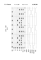
Case 1 - Operation with EQU=1 (STATE = 0)
(RB - even, RE - odd, R0 - Even, EQU = 1)
Summary: R0 loaded with beginning address, RTMP loaded with
beginning address, and R0 passes as address bus signal YAB.
Control circuit 720 sets these variables to the following
values:
Roldymi = 1:
R0 is loaded with value from output signal YM from
first multiplexer 130. (output signal YM here
provides beginning address).
Rbforclsbi = 0:
rtmpldys2i = 0:
rtmpldrbbi = 1:
RTMP is loaded with value from beginning
address register 320 as modified at output
port 320c.
rtmpldyadei = 0:
ybconsti = 1:
YBCONST displacement = 2.
ya2consti = 1:
YACONST displacement = 2.
ymseli = 1:
First multiplexer 130 will allow data output
signal, from beginning address register 320
modified, RBB to pass as YM output signal of first
multiplexer 130.
yabzerolsbi = 0:
When this is 0 the AND circuit 622 does NOT
zero the least significant bit to be provided
as address YAB output signal.
yabseli = 1:
When this is 1 it allows the R0 output signal YADE
to pass through the second multiplexer 620 and to
appear as address bus YAB signal.
Case 2 - First Initialization with EQU=0 (STATE = 1111 = F)
(RB - even, RE - odd, R0 - odd, EQU = 0)
Summary: See Case 1 initialization.
Case 2 - First Interim with EQU=0 (STATE = 0001)
(RB - even, RE - odd, R0 - odd, EQU = 0)
Summary: R0 (first register 122) loading suppressed, RTMP
(second register 222) loaded direct from control circuit 720,
YACONST displacement changes to 1, and RTMP put out as address bus
signal YAB.
Control circuit 720 sets these variables to the following
values:
roldymi = 0:
Suppress loading of R0 from output signal YM.
rbforclsbi = 0:
rtmpldys2i = 1:
This would load an incremented address into
RTMP. A clocked registered output.
rtmpldrbbi = 0:
rtmpldyadei = 0:
ybconsti = 1:
YBCONST displacement = 2.
ya2consti = 0:
YACONST displacement = 1.
ymseli = 0:
First multiplexer 130 will allow data output, from
incremented address from first adder 126 to pass as
YM output signal of first multiplexer 130.
yabzerolsbi = 0:
When this is 0 the AND 622 circuit does NOT
zero the least significant bit to be provided
as address on YAB output signal.
yabseli = 0:
When this is 0 it allows the RTMP output to pass
through the second multiplexer 620 and to appear as
address bus YAB signal.
Case 2 - Operational with EQU=0 (STATE = 0000)
(R0 - even, RE - odd, R0 - odd, EQU = 0)
Summary: R0 (first register 122) loaded with incremented
address from first adder 126, RTMP (second register 222) loaded
with incremented address from second adder 226, RTMP passes as
address bus YAB signal.
Control circuit 720 sets these variables to the following
values:
Roldymi = 1:
R0 loaded from output signal YM of first
multiplexer 130.
Rbforclsbi = 0:
rtmpldys2i = 1:
This would load an incremented address into
RTMP from second adder 226.
rtmpldrbbi = 0:
rtmpldyadei = 0:
ybconsti = 1:
YBCONST displacement = 2.
ya2consti = 1:
YACONST displacement = 2.
ymseli = 0:
First multiplexer 130 will allow data output signal
YS, from incremented address from first adder 126
to pass as YM output signal of first multiplexer
130.
yabzerolsbi = 0:
When this is 0 the AND circuit 622 does NOT
zero the least significant bit to be provided
as address as YAB output signal.
yabseli = 0:
When this is 0 it allows the RTMP output signal
RBUS to pass through the second multiplexer 620 and
to appear as address bus YAB signal.
Case 2 - Operational with EQU=1 (STATE = 0000)
(RB - even, RE - odd, R0 - odd, EQU = 1)
Summary: Only change from Operational with EQU = 0 is that
YACONST is set to 1. The registers R0 and RTMP are not set to the
beginning address value in STATE 0000, another STATE is needed.
Control circuit 720 sets these variables to the following
values:
Roldymi = 1:
R0 loaded from output YM signal of first
multiplexer 130.
Rbforclsbi = 0:
rtmpldys2i = 1:
This would load an incremented address into
RTMP from second adder 126.
rtmpldrbbi = 0:
rtmpldyadei = 0:
ybconsti = 1:
YBCONST displacement = 2.
ya2consti = 0:
YACONST displacement = 1.
ymseli = 0:
First multiplexer 130 will allow data output, from
incremented address from first adder 126 to pass as
YM output signal of first multiplexer 130.
yabzerolsbi = 0:
When this is 0 the AND circuit 622 (AND
circuit 622 includes an AND gate and a
inverter in front of one input) does NOT zero
the least significant bit to be provided as
address as YAB output signal.
yabseli = 0:
When this is 0 it allows the RTMP output to pass
through the second multiplexer 620 and to appear as
address bus YAB signal.
Case 2 - Restart with EQU=1 (STATE = 0010 = 2)
(RB - even, RE - odd, R0 - odd, EQU = 1)
Summary: R0 (first register 122) and RTMP (second register
222) loaded with beginning address modified, i.e. signal RBB, from
beginning address register 320.
Control circuit 720 sets these variables to the following
values:
Roldymi = 1:
R0 loaded from output YM signal of first
multiplexer 130.
Rbforclsbi = 1:
Force the least significant bit of RB on the
RBB bus to be set to "1".
rtmpldys2i = 0:
rtmpldrbbi = 1:
This would load RTMP beginning address from
register 320 modified (RBB).
rtmpldyadei = 0:
ybconsti = 1:
YBCONST displacement = 2.
ya2consti = 0:
YACONST displacement = 1.
ymseli = 1:
First multiplexer 130 will allow data output, from
beginning address register RBB (as modified) to
pass as YM output signal of first multiplexer 130.
yabzerolsbi = 1:
Force the least significant bit of output bus
where YAB signal appears to be cleared, i.e.
to be "0".
yabseli = 0:
When this is 0 it allows the RTMP output signal to
pass through the second multiplexer 620 and to
appear as address bus YAB signal.
Case 3 - First Initialization with EQU=1 (STATE = 1111 = F)
(RB - even, RE - even, R0 - even then odd, EQU = 1)
Summary: See Case 1 Initialization.
Case 3 - Operational with EQU=0 (STATE = 0000)
First Case 3 (RB - even, RE - even, R0 - even (herein even) then
odd, EQU = 1)
Summary: R0 and RTMP loaded with incremented addresses, and
RTMP passes as address bus YAB signal.
Control circuit 720 sets these variables to the following
values:
Roldymi = 1:
R0 loaded from output YM signal of first
multiplexer 130.
Rbforclsbi = 0:
rtmpldys2i = 1:
This would load RTMP with second adder 226
incremented address.
rtmpldrbbi = 0:
rtmpldyadei = 0:
ybconsti = 1:
YBCONST displacement = 2.
ya2consti = 1:
YACONST displacement = 2.
ymseli = 0:
First multiplexer 130 will allow data output, from
first adder 126 to pass as YM output signal of
first multiplexer 130.
yabzerolsbi = 0:
When this is 0 the AND circuit 622 does Not
zero the least significant bit to be provided
as address YAB output signal.
yabseli = 0:
When this is 0 it allows the RTMP output signal
(RBUS) to pass through the second multiplexer 620
and to appear as address bus YAB signal.
Case 3 - Operational with EQU=1 (STATE = 0000)
First Case 3 (RB - even, RE - even, R0 - even (herein even) then
odd, EQU = 1)
Summary: Loading of R0 suppressed, RTMP loaded with beginning
address, (as modified RBB) and RTMP output signal RBUS passes as
Address Bus YAB signal.
Control circuit 720 sets these variables to the following
values:
roldymi = 0:
Suppress R0 loading.
rbforclsbi = 0:
rtmpldys2i = 0:
rtmpldrbbi = 1:
This would load RTMP with modified beginning
address (RBB).
rtmpldyadei = 0:
ybconsti = 1:
YBCONST displacement = 2.
ya2consti = 1:
YACONST displacement = 2.
ymseli = 0:
First Adder 126 data output signal YS passes as YM
output signal.
yabzerolsbi = 0:
Address Bus YAB signal LSB not zeroed.
yabseli = 0:
RTMP output signal (RBUS) passes as Address Bus YAB
signal.
Case 3 - Restart with EQU=1 (STATE = 0011 = 3)
(R0 - even, RE - even, R0 - even (herein even) then odd, EQU = 1)
Summary: R0 loaded with beginning address, RTMP incremented,
and RTMP passes as Address bus YAB signal.
Control circuit 720 sets these variables to the following
values:
roldymi = 1:
R0 loaded from output YM signal.
rbforclsbi = 1:
Need to force R0 to (RB+1) by setting least
significant bit to keep, R0 correct after
wrap.
rtmpldys2i = 1:
RTMP loaded with incremented address from
second adder 226 YS2 output signal.
rtmpldrbbi = 0:
rtmpldyadei = 0:
ybconsti = 1:
YBCONST displacement = 2.
ya2consti = 1:
YA2CONST displacement = 2.
ymseli = 1:
Beginning address output RBB signal passes as YM
output signal.
yabzerolsbi = 0:
Address Bus YAB signal LSB not zeroed.
yabseli = 0:
RTMP output signal (RBUS) passes as Address Bus YAB
signal.
Case 4 - Operational with EQU=0 (STATE = 0011 = 3)
Second Case 4 (RB - even, RE - even, R0 - odd) then odd, EQU = 0)
Summary: R0 and RTMP loaded with incremented addresses, RTMP
passes as address bus YAB signal.
Control circuit 720 sets these variables to the following
values:
roldymi = 1:
R0 loaded from output YM signal.
rbforclsbi = 0:
rtmpldys2i = 1:
RTMP loaded with incremented address from
second adder 226, YS2 output signal.
rtmpldrbbi = 0:
rtmpldyadei = 0:
ybconsti = 1:
YBCONST displacement = 2.
ya2consti = 1:
YACONST displacement = 2.
ymseli = 0:
Incremented address from first adder 126 passes to
YM output signal.
yabzerolsbi = 0:
Address Bus YAB signal LSB not zeroed.
yabseli = 0:
RTMP output passes to Address Bus YAB signal.
Case 4 - Operational with EQU=1 (STATE = 0011 = 3)
Second Case 4 (RB - even, RE - even, R0 - odd) then odd, EQU = 1)
Summary: R0 and RTMP loaded with beginning address (RBB), and
RTMP passes to Address Bus 620c as YAB signal.
Control circuit 720 sets these variables to the following
values:
Roldymi = 1:
R0 loaded from output YM signal.
Rbforclsbi = 0:
rtmpldys2i = 0:
rtmpldrbbi = 1:
RTMP loaded with beginning address RBB.
rtmpldyadei = 0:
ybconsti = 1:
YBCONST displacement = 2.
ya2consti = 1:
YACONST displacement = 2.
ymseli = 1:
Beginning address passes as YM output signal.
yabzerolsbi = 0:
Address Bus YAB signal LSB not zeroed.
yabseli = 0:
RTMP output passes as Address Bus YAB signal.
Case 5 - First Initialization with EQU=1 (STATE = 1111 = F)
(RB - odd, RE - odd, R0 - odd (then even for case 6), EQU = 1)
Summary: See Case 1 Initialization.
Case 5- Interim (STATE = 0100 = 4)
(RB - odd, RE - odd, R0 - odd) then even for case G, EQU = 0)
Summary: R0 suppressed, RTMP loaded with incremented address,
and RTMP passes onto Address Bus YAB signal.
Control circuit 720 sets these variables to the following
values:
r0ldymi = 0:
Suppress R0 loading.
rbforclsbi = 0:
rtmpldys2i = 1:
RTMP loaded with incremented address from
second adder 226, YS2 output signal.
rtmpldrbbi = 0:
rtmpldyadei = 0:
ybconsti = 1:
YBCONST displacement = 2.
ya2consti = 1:
YACONST displacement = 2.
ymseli = 1:
Beginning address RBB passes as YM output signal.
yabzerolsbi = 1:
Address Bus YAB signal LSB zeroed.
yabseli = 0:
RTMP output signal (RBUS) passes as Address Bus YAB
signal.
Case 5- Interim (STATE = 0101 = 5)
(RB - odd, RE - odd, R0 - odd) then even for case 6, EQU = 0)
Summary: R0 loaded with beginning address RBB, RTMP loading
suppressed, and RTMP output passes onto address bus.
Control circuit 720 sets these variables to the following
values:
r0ldymi = 1:
R0 loaded from YM output signal.
Rbforclsbi = 0:
Suppress RTMP loading.
rtmpldys2i = 0:
rtmpldrbbi = 0:
rtmpldyadei = 0:
ybconsti = 1:
YBCONST displacement = 2.
ya2consti = 1:
YACONST displacement = 2.
ymseli = 1:
Beginning address, RBB passes as YM output signal.
yabzerolsbi = 0:
Address Bus YAB signal LSB not zeroed.
yabseli = 0:
RTMP output signal (RBUS) passes as Address Bus YAB
signal.
Case 5- Interim (STATE = 0110 = 6)
(RB - odd, RE - odd, R0 - odd) then even for case 6, EQU = 0)
Summary: R0 loaded with incremented address, RTMP loaded with
incremented address, displacements are set to 1, RTMP passes as
address bus YAB signal.
Control circuit 720 sets these variables to the following
values:
r0ldymi = 1:
R0 loaded from YM output signal.
rbforclsbi = 0:
rtmpldys2i = 1:
RTMP loaded from second adder 226 output YS2
signal.
rtmpldrbbi = 0:
rtmpldyadei = 0:
ybconsti = 0:
YBCONST displacement = 1.
ya2consti = 0:
YACONST displacement = 1.
ymseli = 0:
Incremented address from second adder 226 passes as
YM output signal.
yabzerolsbi = 1:
Address Bus YAB signal LSB zeroed.
yabseli = 0:
RTMP output signal (RBUS) passes as Address Bus YAB
signal.
Case 5- Operational, EQU = 0 (STATE = 0000)
(RB - odd, RE - odd, R0 - odd) then even for case 6, EQU = 0)
Summary: R0 and RTMP loaded with incremented addresses, and
RTMP passes out onto address bus YAB signal.
Control circuit 720 sets these variables to the following
values:
roldymi = 1:
Load R0 with output YM signal.
rbforclsbi = 0:
rtmpldys2i = 1:
RTMP loaded with incremented address from
second adder 226 YS2 output signal.
rtmpldrbbi = 0:
rtmpldyadei = 0:
ybconsti = 1:
YBCONST displacement = 2.
ya2consti = 1:
YACONST displacement = 2.
ymseli = 0:
Incremented address from first adder 126 passes as
YM output signal.
yabzerolsbi = 0:
Address Bus YAB signal LSB not zeroed.
yabseli = 0:
RTMP output signal (RBUS) passes as Address Bus YAB
signal.
Case 5- Operational, EQU = 1 (STATE = 0000)
(RB - odd, RE - odd, R0 - odd) then even for case 6, EQU = 1)
Summary: R0 loaded with Incremented address, RTMP loaded with
beginning address RBB, and RTMP output passes as address bus YAB
signal.
Control circuit 720 sets these variables to the following
values:
r0ldymi = 1:
Load R0 with output YM signal.
rbforclsbi = 0:
rtmpldys2i = 0:
rtmpldrbbi = 1:
RTMP loaded with beginning address RBB.
rtmpldyadei = 0:
ybconsti = 1:
YBCONST displacement = 2.
ya2consti = 1:
YACONST displacement = 2.
ymseli = 0:
Incremented address from first adder 126 passes as
YM output signal.
yabzerolsbi = 0:
Address Bus YAB signal LSB not zeroed.
yabseli = 0:
RTMP output passes as Address Bus YAB signal.
Case 6- Operational, EQU = 0 same as case 5, (STATE = 0000)
(RB - odd, RE - odd, R0 - even) then even for case 6, EQU = 0)
Summary: R0 and RTMP loaded with incremented addresses, and
RTMP passes out onto address bus YAB signal.
Control circuit 720 sets these variables to the following
values:
r0ldymi = 1:
Load R0 with output YM signal.
rbforclsbi = 0:
rtmpldys2i = 0:
RTMP loaded with incremented address from
second adder 226 YS2 output signal.
rtmpldrbbi = 0:
rtmpldyadei = 0:
ybconsti = 1:
YBCONST displacement = 2.
ya2consti = 1:
YA2CONST displacement = 2.
ymseli = 0:
Incremented address from first adder 126 passes as
YM output signal.
yabzerolsbi = 0:
Address Bus YAB signal LSB not zeroed.
yabseli = 0:
RTMP output signal (RBUS) passes as Address Bus YAB
signal.
Case 6- Operational, EQU = 1 (STATE = 0000)
(RB - odd, RE - odd, R0 - even) then even for case 6, EQU = 1)
Summary: R0 loaded with Modified Beginning address RBB, RTMP
loaded with beginning address, and RTMP output passes as address
bus YAB signal.
Control circuit 720 sets these variables to the following
values:
r0ldymi = 1:
Load R0 with output YM signal.
rbforclsbi = 0:
rtmpldys2i = 0:
rtmpldrbbi = 1:
RTMP loaded with beginning address, RBB.
rtmpldyadei = 0:
ybconsti = 1:
YBCONST displacement = 2.
ya2consti = 1:
YA2CONST displacement = 2.
ymseli = 1:
Beginning address passes as YM output signal.
yabzerolsbi = 0:
Address Bus YAB signal LSB not zeroed.
yabseli = 0:
RTMP output passes as Address Bus YAB signal.
Case 7 - First Initialization with EQU=1 (STATE = 1111 = F)
(RB - odd, RE - even, R0 - even)
Summary: See Case 1 Initialization.
Case 7 - Interim (STATE = 0111 = 7)
(RB - odd, RE - even, R0 - even)
Summary: R0 and RTMP loaded with incremented addresses, and
RTMP passes as address bus YAB signal.
Control circuit 720 sets these variables to the following
values:
roldymi = 1:
R0 loaded from YM output signal.
rbforclsbi = 0:
rtmpldys2i = 1:
RTMP loaded from second adder 226 output YS2
signal.
rtmpldrbbi = 0:
rtmpldyadei = 0:
ybconsti = 0:
YBCONST displacement = 1.
ya2consti = 0:
YA2CONST displacement = 1.
ymseli = 0:
Incremented address from second adder 226 passes as
YM output signal.
yabzerolsbi = 0:
Address Bus YAB signal LSB not zeroed.
yabseli = 0:
RTMP output signal (RBUS) passes as Address Bus YAB
signal.
Case 7- Operational , EQU = 0, (STATE = 0000)
(RB - odd, RE - even, R0 - even, EQU = 0)
Summary: R0 and RTMP loaded with incremented addresses, and
RTMP passes out onto address bus.
Control circuit 720 sets these variables to the following
values:
r0ldymi = 1:
Load R0 with output YM signal.
rbforclsbi = 0:
rtmpldys2i = 1:
RTMP loaded with incremented address from
second adder 226 YS2 output signal.
rtmpldrbbi = 0:
rtmpldyadei = 0:
ybconsti = 1:
YBCONST displacement = 2.
ya2consti = 1:
YACONST displacement = 2.
ymseli = 0:
Incremented address from first adder 126 passes as
YM output signal.
yabzerolsbi = 0:
Address Bus YAB signal LSB not zeroed.
yabseli = 0:
RTMP output signal (RBUS) passes as Address Bus YAB
signal.
Case 7- Operational, EQU = 1 (STATE = 0000)
(RB - odd, RE - even, R0 - even, EQU = 1)
Summary: R0 loaded with Beginning address, RTMP loaded with
beginning address, and RTMP output passes to address bus 620c.
Control circuit 720 sets these variables to the following
values:
r0ldymi = 1:
Load R0 with output YM signal.
rbforclsbi = 0:
rtmpldys2i = 0:
rtmpldrbbi = 1:
RTMP loaded with beginning address.
rtmpldyadei = 0:
ybconsti = 1:
YBCONST displacement = 2.
ya2consti = 1:
YA2CONST displacement = 2.
ymseli = 1:
Beginning address RBB passes as YM output signal.
yabzerolsbi = 0:
Address Bus YAB signal LSB not zeroed.
yabseli = 0:
RTMP output passes as Address Bus YAB signal.
Case 8 - First Initialization (STATE = 1111 = F)
(RB - odd, RE - even, R0 - odd)
Summary: See Case 1 Initialization.
Case 8 - Interim (STATE = 0111 = 8)
(RB - odd, RE - even, R0 - odd)
Summary: R0 loading suppressed. RTMP loaded with incremented
addresses, and RTMP passes as address bus YAB signal.
Control circuit 720 sets these variables to the following
values:
r0ldymi = 0:
R0 loading suppressed.
rbforclsbi = 0:
rtmpldys2i = 1:
RTMP loaded from second adder 226 output YS2
signal.
rtmpldrbbi = 0:
rtmpldyadei = 0:
ybconsti = 0:
YBCONST displacement = 1.
ya2consti = 0:
YA2CONST displacement = 1.
ymseli = 0:
Incremented address from second adder 226 passes as
YM output signal.
yabzerolsbi = 0:
Address Bus YAB signal LSB not zeroed.
yabseli = 0:
RTMP output passes as Address Bus YAB signal.
Case 8- Operational (variables set same as case 7 operational),
EQU = 0, (STATE = 0000)
(RB - odd, RE - even, R0 - odd, EQU = 0)
Summary: R0 and RTMP loaded with incremented addresses, and
RTMP passes out onto address bus YAB signal.
Control circuit 720 sets these variables to the following
values:
r0ldymi = 1:
Load R0 with output YM signal.
rbforclsbi = 0:
rtmpldys2i = 1:
RTMP loaded with incremented address from
second adder 226 YS2 output signal.
rtmpldrbbi = 0:
rtmpldyadei = 0:
ybconsti = 1:
YBCONST displacement = 2.
ya2consti = 1:
YACONST displacement = 2.
ymseli = 0:
Incremented address from first adder 126 passes as
YM output signal.
yabzerolsbi = 0:
Address Bus YAB signal LSB not zeroed.
yabseli = 0:
RTMP output passes as Address Bus YAB signal.
Case 8- Operational (variables set same as in case 7), EQU = 1
(STATE = 0000)
(RB - odd, RE - even, R0 - odd, EQU = 1)
Summary: R0 loaded with Beginning address RBB, RTMP loaded
with beginning address RBB, and RTMP output passes as address bus
YAB signal.
Control circuit 720 sets these variables to the following
values:
r0ldymi = 1:
Load R0 with output YM signal.
rbforclsbi = 0:
rtmpldys2i = 0:
rtmpldrbbi = 1:
RTMP loaded with beginning address, RBB.
rtmpldyadei = 0:
ybconsti = 1:
YBCONST displacement = 2.
ya2consti = 1:
YACONST displacement = 2.
ymseli = 1:
Beginning address passes as YM output signal.
yabzerolsbi = 0:
Address Bus YAB signal LSB not zeroed.
yabseli = 0:
RTMP output signal (RBUS) passes to Address Bus YAB
signal.
__________________________________________________________________________
Claims (12)
Priority Applications (1)
| Application Number | Priority Date | Filing Date | Title |
|---|---|---|---|
| US09/044,529 US6148386A (en) | 1998-03-19 | 1998-03-19 | Address generator circuity for a circular buffer |
Applications Claiming Priority (1)
| Application Number | Priority Date | Filing Date | Title |
|---|---|---|---|
| US09/044,529 US6148386A (en) | 1998-03-19 | 1998-03-19 | Address generator circuity for a circular buffer |
Publications (1)
| Publication Number | Publication Date |
|---|---|
| US6148386A true US6148386A (en) | 2000-11-14 |
Family
ID=21932898
Family Applications (1)
| Application Number | Title | Priority Date | Filing Date |
|---|---|---|---|
| US09/044,529 Expired - Fee Related US6148386A (en) | 1998-03-19 | 1998-03-19 | Address generator circuity for a circular buffer |
Country Status (1)
| Country | Link |
|---|---|
| US (1) | US6148386A (en) |
Cited By (4)
| Publication number | Priority date | Publication date | Assignee | Title |
|---|---|---|---|---|
| US20030002376A1 (en) * | 2001-06-29 | 2003-01-02 | Broadcom Corporation | Method and system for fast memory access |
| US20030172246A1 (en) * | 2002-03-11 | 2003-09-11 | Alexander Tessarolo | Circular addressing algorithms providing increased compatibility with one or more higher-level programming languages |
| US6725298B1 (en) * | 1999-06-17 | 2004-04-20 | Nec Electronics Corporation | Method and system for filter-processing by ensuring a memory space for a ring-buffer in digital signal processor |
| US20110131352A1 (en) * | 2009-12-02 | 2011-06-02 | International Business Machines Corporation | Ring Buffer |
Citations (5)
| Publication number | Priority date | Publication date | Assignee | Title |
|---|---|---|---|---|
| US3943492A (en) * | 1972-08-17 | 1976-03-09 | Oak Industries Inc. | Plural storage system |
| US4873667A (en) * | 1987-10-14 | 1989-10-10 | Northern Telecom Limited | FIFO buffer controller |
| US5381360A (en) * | 1993-09-27 | 1995-01-10 | Hitachi America, Ltd. | Modulo arithmetic addressing circuit |
| US5652903A (en) * | 1994-11-01 | 1997-07-29 | Motorola, Inc. | DSP co-processor for use on an integrated circuit that performs multiple communication tasks |
| US5765187A (en) * | 1991-04-05 | 1998-06-09 | Fujitsu Limited | Control system for a ring buffer which prevents overrunning and underrunning |
-
1998
- 1998-03-19 US US09/044,529 patent/US6148386A/en not_active Expired - Fee Related
Patent Citations (5)
| Publication number | Priority date | Publication date | Assignee | Title |
|---|---|---|---|---|
| US3943492A (en) * | 1972-08-17 | 1976-03-09 | Oak Industries Inc. | Plural storage system |
| US4873667A (en) * | 1987-10-14 | 1989-10-10 | Northern Telecom Limited | FIFO buffer controller |
| US5765187A (en) * | 1991-04-05 | 1998-06-09 | Fujitsu Limited | Control system for a ring buffer which prevents overrunning and underrunning |
| US5381360A (en) * | 1993-09-27 | 1995-01-10 | Hitachi America, Ltd. | Modulo arithmetic addressing circuit |
| US5652903A (en) * | 1994-11-01 | 1997-07-29 | Motorola, Inc. | DSP co-processor for use on an integrated circuit that performs multiple communication tasks |
Non-Patent Citations (2)
| Title |
|---|
| <jljackso@mail.dimensional.com> Re: Help! Strcpy()-like function that eliminates unwanted strings? News://comp.lang.c Jul. 10, 1996. |
| jljackso mail.dimensional.com Re: Help Strcpy() like function that eliminates unwanted strings News://comp.lang.c Jul. 10, 1996. * |
Cited By (9)
| Publication number | Priority date | Publication date | Assignee | Title |
|---|---|---|---|---|
| US6725298B1 (en) * | 1999-06-17 | 2004-04-20 | Nec Electronics Corporation | Method and system for filter-processing by ensuring a memory space for a ring-buffer in digital signal processor |
| US20030002376A1 (en) * | 2001-06-29 | 2003-01-02 | Broadcom Corporation | Method and system for fast memory access |
| US6912173B2 (en) * | 2001-06-29 | 2005-06-28 | Broadcom Corporation | Method and system for fast memory access |
| US20050180240A1 (en) * | 2001-06-29 | 2005-08-18 | Broadcom Corporation | Method and system for fast memory access |
| US20030172246A1 (en) * | 2002-03-11 | 2003-09-11 | Alexander Tessarolo | Circular addressing algorithms providing increased compatibility with one or more higher-level programming languages |
| US7039789B2 (en) * | 2002-03-11 | 2006-05-02 | Texas Instruments Incorporated | Circular addressing algorithms providing increased compatibility with one or more higher-level programming languages |
| US20110131352A1 (en) * | 2009-12-02 | 2011-06-02 | International Business Machines Corporation | Ring Buffer |
| US8291136B2 (en) * | 2009-12-02 | 2012-10-16 | International Business Machines Corporation | Ring buffer |
| US8516170B2 (en) * | 2009-12-02 | 2013-08-20 | International Business Machines Corporation | Control flow in a ring buffer |
Similar Documents
| Publication | Publication Date | Title |
|---|---|---|
| DE69233412T2 (en) | Device and computer program product for executing branch instructions | |
| KR100348951B1 (en) | Memory store from a register pair conditional | |
| US5222240A (en) | Method and apparatus for delaying writing back the results of instructions to a processor | |
| US6006315A (en) | Computer methods for writing a scalar value to a vector | |
| US10318300B2 (en) | Parsing-enhancement facility | |
| PT803091E (en) | INFORMATION SYSTEM | |
| JP2006079652A (en) | Data processing by multiple instruction sets | |
| US5669012A (en) | Data processor and control circuit for inserting/extracting data to/from an optional byte position of a register | |
| US6332152B1 (en) | Arithmetic unit and data processing unit | |
| US5787025A (en) | Method and system for performing arithmetic operations with single or double precision | |
| US6073228A (en) | Modulo address generator for generating an updated address | |
| US5757685A (en) | Data processing system capable of processing long word data | |
| US6148386A (en) | Address generator circuity for a circular buffer | |
| US20080148018A1 (en) | Shift Processing Unit | |
| US5539900A (en) | Information processing system | |
| US5276822A (en) | System with enhanced execution of address-conflicting instructions using immediate data latch for holding immediate data of a preceding instruction | |
| US5938758A (en) | Microprocessor having function of prefetching instruction | |
| US4641278A (en) | Memory device with a register interchange function | |
| EP0278529A2 (en) | Multiplication circuit capable of operating at a high speed with a small amount of hardware | |
| US4975835A (en) | Variable length data processing apparatus for consecutively processing variable-length data responsive to one instruction | |
| EP0334131B1 (en) | Data processor performing operation on data having length shorter than one-word length | |
| US7631166B1 (en) | Processing instruction without operand by inferring related operation and operand address from previous instruction for extended precision computation | |
| US4212058A (en) | Computer store mechanism | |
| US6005502A (en) | Method for reducing the number of bits needed for the representation of constant values in a data processing device | |
| JP2530873B2 (en) | Instruction prefetch address update circuit |
Legal Events
| Date | Code | Title | Description |
|---|---|---|---|
| AS | Assignment |
Owner name: LUCENT TECHNOLOGIES INC., NEW JERSEY Free format text: ASSIGNMENT OF ASSIGNORS INTEREST;ASSIGNORS:RHODES, DOUGLAS;THIERBACH, MARK;REEL/FRAME:009055/0218 Effective date: 19980312 |
|
| FEPP | Fee payment procedure |
Free format text: PAYOR NUMBER ASSIGNED (ORIGINAL EVENT CODE: ASPN); ENTITY STATUS OF PATENT OWNER: LARGE ENTITY |
|
| AS | Assignment |
Owner name: THE CHASE MANHATTAN BANK, AS COLLATERAL AGENT, TEX Free format text: CONDITIONAL ASSIGNMENT OF AND SECURITY INTEREST IN PATENT RIGHTS;ASSIGNOR:LUCENT TECHNOLOGIES INC. (DE CORPORATION);REEL/FRAME:011722/0048 Effective date: 20010222 |
|
| REMI | Maintenance fee reminder mailed | ||
| LAPS | Lapse for failure to pay maintenance fees | ||
| STCH | Information on status: patent discontinuation |
Free format text: PATENT EXPIRED DUE TO NONPAYMENT OF MAINTENANCE FEES UNDER 37 CFR 1.362 |
|
| FP | Lapsed due to failure to pay maintenance fee |
Effective date: 20041114 |
|
| AS | Assignment |
Owner name: LUCENT TECHNOLOGIES INC., NEW JERSEY Free format text: TERMINATION AND RELEASE OF SECURITY INTEREST IN PATENT RIGHTS;ASSIGNOR:JPMORGAN CHASE BANK, N.A. (FORMERLY KNOWN AS THE CHASE MANHATTAN BANK), AS ADMINISTRATIVE AGENT;REEL/FRAME:018590/0287 Effective date: 20061130 |