EP0504837B1 - Verfahren und Vorrichtung für die Herstellung eines Silizium-Einkristalls - Google Patents
Verfahren und Vorrichtung für die Herstellung eines Silizium-Einkristalls Download PDFInfo
- Publication number
- EP0504837B1 EP0504837B1 EP92104679A EP92104679A EP0504837B1 EP 0504837 B1 EP0504837 B1 EP 0504837B1 EP 92104679 A EP92104679 A EP 92104679A EP 92104679 A EP92104679 A EP 92104679A EP 0504837 B1 EP0504837 B1 EP 0504837B1
- Authority
- EP
- European Patent Office
- Prior art keywords
- single crystal
- silicon single
- main chamber
- disposed
- silicon
- Prior art date
- Legal status (The legal status is an assumption and is not a legal conclusion. Google has not performed a legal analysis and makes no representation as to the accuracy of the status listed.)
- Expired - Lifetime
Links
- XUIMIQQOPSSXEZ-UHFFFAOYSA-N Silicon Chemical compound [Si] XUIMIQQOPSSXEZ-UHFFFAOYSA-N 0.000 title claims description 87
- 229910052710 silicon Inorganic materials 0.000 title claims description 87
- 239000010703 silicon Substances 0.000 title claims description 87
- 239000013078 crystal Substances 0.000 title claims description 86
- 238000000034 method Methods 0.000 title claims description 24
- VYPSYNLAJGMNEJ-UHFFFAOYSA-N silicon dioxide Inorganic materials O=[Si]=O VYPSYNLAJGMNEJ-UHFFFAOYSA-N 0.000 claims description 18
- 239000012212 insulator Substances 0.000 claims description 17
- 239000010453 quartz Substances 0.000 claims description 15
- OKTJSMMVPCPJKN-UHFFFAOYSA-N Carbon Chemical compound [C] OKTJSMMVPCPJKN-UHFFFAOYSA-N 0.000 claims description 9
- 238000010438 heat treatment Methods 0.000 claims description 9
- 239000000155 melt Substances 0.000 claims description 7
- 229910002804 graphite Inorganic materials 0.000 claims description 6
- 239000010439 graphite Substances 0.000 claims description 6
- 239000011810 insulating material Substances 0.000 claims description 6
- 230000007246 mechanism Effects 0.000 claims description 6
- 238000010926 purge Methods 0.000 claims description 6
- 239000002131 composite material Substances 0.000 claims description 3
- 230000000717 retained effect Effects 0.000 claims description 3
- 230000015556 catabolic process Effects 0.000 description 33
- 235000012431 wafers Nutrition 0.000 description 26
- 230000002950 deficient Effects 0.000 description 12
- 230000000052 comparative effect Effects 0.000 description 10
- 230000007547 defect Effects 0.000 description 7
- 238000009826 distribution Methods 0.000 description 6
- 230000009467 reduction Effects 0.000 description 6
- 238000004519 manufacturing process Methods 0.000 description 4
- 238000010276 construction Methods 0.000 description 3
- 229910052814 silicon oxide Inorganic materials 0.000 description 3
- 239000000126 substance Substances 0.000 description 3
- XKRFYHLGVUSROY-UHFFFAOYSA-N Argon Chemical compound [Ar] XKRFYHLGVUSROY-UHFFFAOYSA-N 0.000 description 2
- 238000002474 experimental method Methods 0.000 description 2
- 239000011261 inert gas Substances 0.000 description 2
- 238000003754 machining Methods 0.000 description 2
- 238000002844 melting Methods 0.000 description 2
- 230000008018 melting Effects 0.000 description 2
- 238000005498 polishing Methods 0.000 description 2
- 229910021420 polycrystalline silicon Inorganic materials 0.000 description 2
- LIVNPJMFVYWSIS-UHFFFAOYSA-N silicon monoxide Chemical group [Si-]#[O+] LIVNPJMFVYWSIS-UHFFFAOYSA-N 0.000 description 2
- 229920000049 Carbon (fiber) Polymers 0.000 description 1
- LIXXICXIKUPJBX-UHFFFAOYSA-N [Pt].[Rh].[Pt] Chemical compound [Pt].[Rh].[Pt] LIXXICXIKUPJBX-UHFFFAOYSA-N 0.000 description 1
- 229910052786 argon Inorganic materials 0.000 description 1
- QVGXLLKOCUKJST-UHFFFAOYSA-N atomic oxygen Chemical compound [O] QVGXLLKOCUKJST-UHFFFAOYSA-N 0.000 description 1
- 229910052799 carbon Inorganic materials 0.000 description 1
- 239000004917 carbon fiber Substances 0.000 description 1
- 238000001816 cooling Methods 0.000 description 1
- 238000000151 deposition Methods 0.000 description 1
- 230000008021 deposition Effects 0.000 description 1
- 230000000694 effects Effects 0.000 description 1
- 238000000407 epitaxy Methods 0.000 description 1
- 238000005530 etching Methods 0.000 description 1
- 239000007789 gas Substances 0.000 description 1
- 230000006872 improvement Effects 0.000 description 1
- 230000010354 integration Effects 0.000 description 1
- 239000000463 material Substances 0.000 description 1
- 238000005259 measurement Methods 0.000 description 1
- VNWKTOKETHGBQD-UHFFFAOYSA-N methane Chemical compound C VNWKTOKETHGBQD-UHFFFAOYSA-N 0.000 description 1
- 230000003287 optical effect Effects 0.000 description 1
- 230000003647 oxidation Effects 0.000 description 1
- 238000007254 oxidation reaction Methods 0.000 description 1
- 239000001301 oxygen Substances 0.000 description 1
- 229910052760 oxygen Inorganic materials 0.000 description 1
- 229920005591 polysilicon Polymers 0.000 description 1
- KMUONIBRACKNSN-UHFFFAOYSA-N potassium dichromate Chemical compound [K+].[K+].[O-][Cr](=O)(=O)O[Cr]([O-])(=O)=O KMUONIBRACKNSN-UHFFFAOYSA-N 0.000 description 1
- 230000008569 process Effects 0.000 description 1
- 239000004065 semiconductor Substances 0.000 description 1
- 239000000758 substrate Substances 0.000 description 1
- 238000011179 visual inspection Methods 0.000 description 1
- XLYOFNOQVPJJNP-UHFFFAOYSA-N water Substances O XLYOFNOQVPJJNP-UHFFFAOYSA-N 0.000 description 1
Images



Classifications
-
- C—CHEMISTRY; METALLURGY
- C30—CRYSTAL GROWTH
- C30B—SINGLE-CRYSTAL GROWTH; UNIDIRECTIONAL SOLIDIFICATION OF EUTECTIC MATERIAL OR UNIDIRECTIONAL DEMIXING OF EUTECTOID MATERIAL; REFINING BY ZONE-MELTING OF MATERIAL; PRODUCTION OF A HOMOGENEOUS POLYCRYSTALLINE MATERIAL WITH DEFINED STRUCTURE; SINGLE CRYSTALS OR HOMOGENEOUS POLYCRYSTALLINE MATERIAL WITH DEFINED STRUCTURE; AFTER-TREATMENT OF SINGLE CRYSTALS OR A HOMOGENEOUS POLYCRYSTALLINE MATERIAL WITH DEFINED STRUCTURE; APPARATUS THEREFOR
- C30B29/00—Single crystals or homogeneous polycrystalline material with defined structure characterised by the material or by their shape
- C30B29/02—Elements
- C30B29/06—Silicon
-
- C—CHEMISTRY; METALLURGY
- C30—CRYSTAL GROWTH
- C30B—SINGLE-CRYSTAL GROWTH; UNIDIRECTIONAL SOLIDIFICATION OF EUTECTIC MATERIAL OR UNIDIRECTIONAL DEMIXING OF EUTECTOID MATERIAL; REFINING BY ZONE-MELTING OF MATERIAL; PRODUCTION OF A HOMOGENEOUS POLYCRYSTALLINE MATERIAL WITH DEFINED STRUCTURE; SINGLE CRYSTALS OR HOMOGENEOUS POLYCRYSTALLINE MATERIAL WITH DEFINED STRUCTURE; AFTER-TREATMENT OF SINGLE CRYSTALS OR A HOMOGENEOUS POLYCRYSTALLINE MATERIAL WITH DEFINED STRUCTURE; APPARATUS THEREFOR
- C30B15/00—Single-crystal growth by pulling from a melt, e.g. Czochralski method
- C30B15/14—Heating of the melt or the crystallised materials
-
- Y—GENERAL TAGGING OF NEW TECHNOLOGICAL DEVELOPMENTS; GENERAL TAGGING OF CROSS-SECTIONAL TECHNOLOGIES SPANNING OVER SEVERAL SECTIONS OF THE IPC; TECHNICAL SUBJECTS COVERED BY FORMER USPC CROSS-REFERENCE ART COLLECTIONS [XRACs] AND DIGESTS
- Y10—TECHNICAL SUBJECTS COVERED BY FORMER USPC
- Y10S—TECHNICAL SUBJECTS COVERED BY FORMER USPC CROSS-REFERENCE ART COLLECTIONS [XRACs] AND DIGESTS
- Y10S117/00—Single-crystal, oriented-crystal, and epitaxy growth processes; non-coating apparatus therefor
- Y10S117/90—Apparatus characterized by composition or treatment thereof, e.g. surface finish, surface coating
-
- Y—GENERAL TAGGING OF NEW TECHNOLOGICAL DEVELOPMENTS; GENERAL TAGGING OF CROSS-SECTIONAL TECHNOLOGIES SPANNING OVER SEVERAL SECTIONS OF THE IPC; TECHNICAL SUBJECTS COVERED BY FORMER USPC CROSS-REFERENCE ART COLLECTIONS [XRACs] AND DIGESTS
- Y10—TECHNICAL SUBJECTS COVERED BY FORMER USPC
- Y10T—TECHNICAL SUBJECTS COVERED BY FORMER US CLASSIFICATION
- Y10T117/00—Single-crystal, oriented-crystal, and epitaxy growth processes; non-coating apparatus therefor
- Y10T117/10—Apparatus
- Y10T117/1024—Apparatus for crystallization from liquid or supercritical state
- Y10T117/1032—Seed pulling
- Y10T117/1068—Seed pulling including heating or cooling details [e.g., shield configuration]
Definitions
- the present invention relates to a method according to the preamble of claim 1 and apparatus as according to the preamble of claims 3 and 7 for producing a silicon single crystal having an excellent dielectric breakdown strength of the silicon oxide film formed thereon.
- a silicon single crystal grown by a pulling method commonly called the Czochralski (CZ) method is produced by an apparatus which comprises a main chamber having a side wall and a top wall disposed on an upper end of the side wall and having an open central portion extending upwardly so as to form a neck portion at an upper end of the main chamber, a quartz crucible disposed in the main chamber with a heater and a thermal shield disposed between the quartz crucible and the side wall of the main chamber, and a gate valve, a pull chamber and a crystal pulling mechanism that are disposed above the neck of the main chamber for pulling a growing silicon single crystal from a silicon melt retained in the quartz crucible.
- CZ Czochralski
- CZ wafers single crystal wafers prepared from the Czochralski-grown silicon single crystal have an oxide film dielectric breakdown strength which is much smaller than that of single crystal wafers (FZ wafers) prepared from a silicon single crystal grown by the float-zone (FZ) method and wafers (epitaxial wafers) with a silicon film grown by epitaxy on a single crystal substrate prepared by the CZ method.
- FZ wafers single crystal wafers
- FZ wafers float-zone
- wafers epitaxy on a single crystal substrate prepared by the CZ method.
- the CZ wafers are widely used as a material for fabricating electronic devices.
- MOS device having a highly reliable gate oxide film had increased. Since the reliability of the gate oxide film is influenced very much by the oxide film dielectric breakdown strength, there is a great need for a CZ wafer having an excellent oxide film dielectric breakdown strength.
- a CZ wafer having an excellent oxide film dielectric breakdown strength can be produced by controlling the pulling rate (i.e., the crystal growth rate) of a silicon single crystal below 0.8 mm/min.
- US-A-4 956 153 shows an apparatus for growing a single crystal of semiconductor silicon by the Czochralski method which apparatus comprises a heat resistant and heat insulating covering board, which are heated in order to prevent deposition of silicon monoxide which could otherwise deposit there and eventually fall off and contaminate the silicon melt located underneath.
- the temperature gradient of the melt of silicon at and in the vicinity of the interface with the growing single crystal is increased by efficiently removing the heat from the interface, which is achieved by a cooling effect by means of argon gas flowing through the heat insulating cylindrical tube.
- the provision of a certain temperature gradient for achieving silicon single crystals having a good oxide film dielectric breakdown strength is not known.
- the grown silicon single crystal has an insufficient silicon oxide film dielectric breakdown strength.
- the pulling rate is set in the range of 0.8 - 2 mm/min. This combination increases the oxide film dielectric breakdown strength and productivity of the silicon single crystal. A pulling rate (i.e., a crystal growth rate) less than 0.8 mm/min lowers the productivity of the silicon single crystal. Conversely, a pulling rate greater than 2 mm/min may affect the oxide film dielectric breakdown strength.
- Another object of the present invention is to provide an apparatus for carrying out the method. This object is solved by apparatuses of the initially specified type having the features as set out in the characterising portions of independent claims 3 or 7.
- the heat insulator extends between a lower end of the neck portion of the main chamber and an upper end of the thermal shield. From the viewpoint of the heat insulating efficiency, a heat insulator having a dome-like shape is preferable.
- the heat insulator preferably has a composite structure composed of a graphite and a heat-insulating material. The graphite constitutes an inner lining of the heat-insulating material.
- a purge tube depending from a lower end of the neck may be provided for increasing the temperature gradient of only a portion of the growing silicon single crystal located near the silicon melt surface.
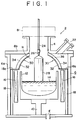
- FIG. 1 shows an apparatus 2 for producing a silicon single crystal grown by Czochralski (CZ) method according to a first embodiment of this invention.
- the apparatus 2 includes a main chamber 6 having a reduced diameter portion or neck 4 at its upper end.
- the main chamber 6 has an annular side wall 6a and an upper wall 6b disposed on an upper end of the side wall 6a.
- the upper wall 6b has an open central portion extending upwardly to form the neck portion 4 of the main chamber 6.
- a pull chamber (not shown) is disposed above the main chamber 6 with a gate valve 8 disposed therebetween.
- a crystal pulling mechanism (not shown) for pulling a growing silicon crystal 28.
- the pull chamber and the crystal pulling mechanism are known in the art and, hence, description and illustration thereof can be omitted.
- the main chamber 6 receives therein a quartz crucible 12 rotatably supported by a vertical support shaft 10.
- the quartz crucible 12 contains a melt 14 of polycrystalline silicon.
- the quartz crucible 12 is heated by a heater 16 disposed around the quartz crucible 12.
- the heater 16 surrounded by a thermal shield 18 extending along an inside surface of the side wall 6a of the main chamber 6.
- the top wall 6b of the main chamber 6 is provided with a view port 22 for enabling observation of the interior of the main chamber 6.
- the main chamber 6 as a whole has a water jacket structure to prevent undue temperature rise.
- a pulling means comprising a pull shaft 24 extends vertically downward from the crystal lift mechanism through the pull chamber into the main chamber 6.
- a seed crystal 26 is attached to a forward end of the pull shaft 24.
- the pull shaft 24 is vertically movable to dip the seed crystal 26 into the silicon melt 14 and then gradually pull the seed crystal 26 upwardly from the silicon melt 14 while rotating the seed crystal 26, so that a silicon single crystal 28 grown by the CZ method is produced.
- the pull shaft 24 may be replaced by a flexible pulling means such as a pull wire.
- Reference character H designates a hot zone extending above the silicon melt 14 in the quartz crucible 12.
- the hot zone H is surrounded by an upper portion of the side wall 6a and the upper wall 6b of the main chamber 6.
- the main chamber 6 has an exhaust hole E connected with a vacuum pump (not shown).
- the exhaust hole E is used for exhausting an inert gas filled in the main chamber 6 and controlling the pressure of the inert gas.
- the apparatus 2 further includes a heat insulator 30 for keeping the temperature of an upper part of the hot zone H.
- the heat insulator 30 has a composite structure composed of a graphite 32 and a heat-insulating material 34 such as a carbon fiber heat-insulator sold under the tradename "KURECA” manufactured by Kureha Chemical Industry Co., Ltd.
- the graphite 32 constitutes an inner lining of the heat-insulating material 34.
- the heat insulator 30 has a dome-like shape and extends between a lower end of the neck portion 4 and an upper end or an upper end extension 18a of the thermal shield plate 18 to interconnect the neck portion 4 and the thermal shield plate 18.
- the heat insulator 30 has a view hole 36 aligned with the view port 22 for the purpose of observing the interior of the main chamber 6.
- the shape of the heat insulator 30 is not limited to the dome-like shape.
- the heat insulator 30 may be formed in a cup-like shape composed of a vertical portion extending along the inside surface of the side wall 6a, and a horizontal portion lying over an inside surface of the top wall 6b.
- the dome-like heat insulator 30, serving as means for keeping the temperature of the upper part of the hot zone H, may be replaced by a second heater 38 for heating the growing silicon single crystal 28, as shown in FIG. 2.
- the second heater 38 is disposed above the heater 16 (main heater) for heating the quartz crucible 12.
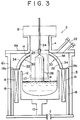
- the apparatus further includes a purge tube 40 (FIG. 3) which may be provided in combination with the dome-like heat insulator 30 shown in FIG. 1, or alternatively in combination with the second heater 38 shown in FIG. 2.
- the purge tube 40 depends from a lower end of the neck portion 4 so as to cover a portion of the growing silicon single crystal 28 located adjacent to the melt surface for increasing the temperature gradient only of this portion of the growing silicon single crystal 28.
- a silicon single crystal grown by Czochralski (CZ) method was pulled under the following conditions by using a conventional CZ equipment. During the pulling process, the silicon single crystal was removed from a furnace. After a platinum-rhodium platinum thermocouple was embedded in the removed silicon single crystal, the temperature distribution of a portion of the silicon single crystal extending upwardly from the silicon melt surface was measured. The results obtained are shown in FIG. 4. As indicated by the broken line (Prior Art) shown in FIG. 4, a portion of the growing silicon single crystal having a temperature ranging from 1150 to 1420°C (i.e., the melting point of silicon) had a length (equal to the distance from the melt surface) not greater than 280 mm.
- CZ Czochralski
- the pulling rate (crystal growth rate) was changed within the range of 0.4 - 1.6 mm/min to form various samples of silicon single crystal.
- the samples were processed into silicon wafers by effected the same machining processes and chemical polishing as done in the fabrication of commercial silicon wafers of 600 - 700 ⁇ m thick.
- the silicon wafers were inspected to determine the defect density and the oxide film dielectric breakdown strength in conjunction with the crystal growth rate (pulling rate). The results obtained are shown in FIGS. 5 - 7.
- each wafer was etched for 30 min by a preferential etching method [2 g: K2Cr2O7, 30 mL: H2O, 100 mL: HF, Secco'd Aragona, : J. Electrochem. Soc., 119, 948 (1972)].
- a preferential etching method [2 g: K2Cr2O7, 30 mL: H2O, 100 mL: HF, Secco'd Aragona, : J. Electrochem. Soc., 119, 948 (1972)].
- each of the devices had a polysilicon gate having an area of 8 mm, and a 25 nm (250 ⁇ ) oxide layer formed by oxidation at 900°C for 100 min in dry oxygen atmosphere.
- a dielectric breakdown test was made for each device and a device whose oxide layer having a dielectric breakdown strength greater than 8 MV/cm was evaluated as a non-defective device. Then, a percentage of the non-defective devices was given as representing the oxide film dielectric breakdown strength.
- FIG. 5 The relation between the crystal growth rate and the density of wave marks counted as specified above with respect to the silicon wafers according to the Comparative Example is shown in FIG. 5.
- the wave mark density is 20 pieces/cm when the pulling rate is as low as 0.4 mm/min.
- the wave mark density is increased to more than 1000 pieces/cm.
- the relation between the wave mark density and the percent non-defective of oxide film dielectric breakdown strength taken with respect to the silicon wafers of the Comparative Example is shown in FIG. 6.
- the distribution of circles (Prior Art) shown in FIG. 6 indicates that those silicon wafers having a high wave mark density such as 1000 pieces/cm have a percent non-defective of oxide film dielectric breakdown strength nearly equal to 40%.
- the silicon wafers having a wave mark density of about 200 pieces/cm have a percent non-defective of oxide film dielectric breakdown strength approximately equal to 80%.
- the relation between the crystal growth rate and the percent non-defective of oxide film dielectric breakdown strength of the silicon wafers according to the Comparative Example is shown in FIG. 7.
- the percent non-defective of oxide film dielectric breakdown strength is 80% when the crystal growth rate is relatively low such as 0.4 mm/min.
- the percent non-defective of oxide film dielectric breakdown strength is reduced to about 50%.
- a low crystal growth rate is an essential condition in order to produce a silicon single crystal having an excellent oxide film dielectric breakdown strength.
- the low crystal growth rate results in a considerable reduction in productivity of the silicon single crystal and hence is not practically useful.
- a silicon single crystal grown by the CZ method was produced under the same conditions as the Comparative Example with the exception that the conventional CZ equipment was replaced by the apparatus of the present invention described above.
- a measurement was made in the same manner as the Comparative Example for determining the temperature distribution of a portion of the silicon single crystal disposed above the melt surface.
- the results obtained are shown in FIG. 4.
- a portion of the silicon single crystal in the temperature range of from 1150 to 1420°C i.e., the melting point of silicon
- two samples of silicon single crystal were pulled at different rates 0.9 mm/min and 1.2 mm/min, respectively. These samples were processed into 600 - 700 ⁇ m thickness silicon wafers by effecting the same machining processes and chemical polishing as done in the Comparative Example and also in the fabrication of commercial silicon wafers.
- the defect density and oxide film dielectric break-down strength of the fabricated silicon wafers were inspected in conjunction with the crystal growth rate (pulling rate). The results obtained are shown in FIGS. 5 through 7.
- the wave mark density observed at the crystal growth rate of 1.2 mm/min is 100 pieces/cm which is smaller by one digit than the wave mark density of Comparative Example (Prior Art).
- An additional reduction in wave mark density (20 pieces/cm) is obtained when the crystal growth rate is 0.9 mm/min.
- Two triangles shown in FIG. 6 indicate that the silicon wafers according to the Inventive Example have a wave mark density smaller than 100 pieces/cm and a percent non-defective of oxide film dielectric breakdown strength equal to 80%.
- the percent non-defective of oxide film dielectric breakdown strength of the Inventive Example is not smaller than 80% irrespective of the crystal growth rate.
- a comparison made with respect to the same crystal growth rate 1.2 mm/min indicates that the Inventive Example (having a longer thermal history in the temperature range above 1150°) has an oxide film dielectric breakdown strength which is twice as large as that of the Comparative Example (having a shorter thermal history in the temperature range above 1150°C).
- a silicon single crystal having an excellent oxide film dielectric breakdown strength can be produced stably with high yield and high productivity.
Landscapes
- Chemical & Material Sciences (AREA)
- Engineering & Computer Science (AREA)
- Crystallography & Structural Chemistry (AREA)
- Materials Engineering (AREA)
- Metallurgy (AREA)
- Organic Chemistry (AREA)
- Crystals, And After-Treatments Of Crystals (AREA)
Claims (8)
- Ein Verfahren zum Herstellen eines durch das Czochralski-Verfahren gewachsenen Silizium-Einkristalls, wobei der Silizium-Einkristall durch Ziehen nach oben aus einer Siliziumschmelze (14) gewachsen wird,
gekennzeichnet durch
Einstellen und Aufrechterhalten der Ziehbedingungen derart, daß ein Teil des wachsenden Silizium-Einkristalls (28), der eine Temperatur in dem Bereich von 1420°C bis 1150°C aufweist, eine Länge von mehr als 280 mm aufweist, wobei diese Länge von der Oberfläche der Schmelze nach oben gemessen wird. - Ein Verfahren gemäß Anspruch 1, wobei der wachsende Silizium-Einkristall (28) bei einer Ziehgeschwindigkeit in dem Bereich von 0,8 - 2 mm/min gezogen wird.
- Eine Vorrichtung zum Ausführen des Verfahrens nach Anspruch 1 mit:einer Hauptkammer (6), die eine Seitenwand (6a) und eine an einem oberen Ende der Seitenwand (6a) angebrachte obere Wand (6b) aufweist, wobei die obere Wand (6b) einen offenen zentralen Schnitt aufweist, der sich derart nach oben erstreckt, daß ein Halsabschnitt (4) an einem oberen Ende der Hauptkammer (6) gebildet wird;einem Quarztiegel (12), der in der Hauptkammer (6) vorgesehen ist, mit einer Heizvorrichtung (16) und einem in der dargelegten Reihenfolge vorgesehenen thermischen Schild (18), das zwischen dem Quarztiegel (12) und der Seitenwand (6a) der Hauptkammer (6) vorgesehen ist; undeinem Pfortenventil (8), einer Ziehkammer und einem Kristallanhebemechanismus, die oberhalb des Halsabschnitts (4) der Hauptkammer (6) in der dargelegten Reihenfolge vorgesehen sind, zum Ziehen eines wachsenden Silizium-Einkristalls (28) nach oben aus einer Siliziumschmelze (14), die sich in dem Quarztiegel (12) befindet,dadurch gekennzeichnet,daß eine Wärmeisolationsvorrichtung (30) in der Hauptkammer (6) vorgesehen ist zum Aufrechterhalten einer hohen Temperatur eines Bereiches, der den wachsenden Silizium-Einkristall (28) umgibt, wobei der Bereich dadurch weiter nach oben von der Oberfläche der Siliziumschmelze ausgedehnt wird, um dadurch den wachsenden Kristall (28) über eine Länge von wenigstens 280 mm, die von der Oberfläche (14) der Schmelze nach oben gemessen wird, bei einer Temperatur in dem Bereich zwischen 1150°C und 1420°C zu halten.
- Eine Vorrichtung gemäß Anspruch 3, dadurch gekennzeichnet, daß ein unteres Ende des Halsabschnitts (4) und ein oberes Ende (18a) des thermischen Schilds (18) durch die Wärmeisolationsvorrichtung (30) verbunden sind.
- Eine Vorrichtung gemäß Anspruch 3 oder 4, wobei die Wärmeisolationsvorrichtung eine kuppelartige Form aufweist.
- Eine Vorrichtung gemäß einem der vorhergehenden Ansprüche 3 - 5, wobei die Wärmeisolationsvorrichtung (30) eine zusammengesetzte Bauart aufweist, die aus Graphit (32) und einem Wärmeisolationsmaterial (34) zusammengesetzt ist, wobei der Graphit (32) eine innere Auskleidung des Wärmeisolationsmaterials (34) bildet.
- Eine Vorrichtung zum Ausführen des Verfahrens nach Anspruch 1 mit:einer Hauptkammer (6), die eine Seitenwand (6a) und eine auf einem oberen Ende der Seitenwand (6a) vorgesehene obere Wand (6b) aufweist, wobei die obere Wand einen offenen zentralen Bereich aufweist, der sich nach oben derart erstreckt, daß ein Halsabschnitt (4) an einem oberen Ende der Hauptkammer (6) gebildet wird;einem Quarztiegel (12), der in der Hauptkammer (6) angeordnet ist, mit einer Heizeinrichtung (16) und einem in der genannten Reihenfolge vorgesehenen thermischen Schild (18), das zwischen dem Quarztiegel (12) und der Seitenwand (6a) der Hauptkammer (6) angeordnet ist; undeinem Pfortenventil (8), einer Ziehkammer und einem Kristallanhebemechanismus, die über dem Halsabschnitt (4) der Hauptkammer (6) in der genannten Reihenfolge vorgesehen sind zum Ziehen eines wachsenden Silizium-Einkristalls (28) nach oben aus einer Siliziumschmelze (14), die sich in dem Quarztiegel (12) befindet,dadurch gekennzeichnet,eine zweite Heizvorrichtung (38) über der ersten Heizvorrichtung (16) vorgesehen ist zum Heizen des wachsenden Silizium-Einkristalls (28) derart, daß der wachsende Silizium-Einkristall (28) eine Temperatur in dem Bereich von 1420°C bis 1150°C über eine Länge von wenigstens 280 mm aufweist, die von der Oberfläche der Siliziumschmelze nach oben gemessen wird.
- Eine Vorrichtung gemäß einem der vorhergehenden Ansprüche 3 - 7, die weiter ein Spülrohr (40) enthält, das von einem unteren Ende des Halsabschnitts (4) herabhängt zum Erhöhen des Temperaturgradienten dx/dT lediglich eines Teils des wachsenden Silizium-Einkristalls (28), der in der Nähe der Oberfläche der Siliziumschmelze gelegen ist.
Applications Claiming Priority (2)
| Application Number | Priority Date | Filing Date | Title |
|---|---|---|---|
| JP81837/91 | 1991-03-20 | ||
| JP3081837A JP3016897B2 (ja) | 1991-03-20 | 1991-03-20 | シリコン単結晶の製造方法及び装置 |
Publications (3)
| Publication Number | Publication Date |
|---|---|
| EP0504837A2 EP0504837A2 (de) | 1992-09-23 |
| EP0504837A3 EP0504837A3 (en) | 1993-02-17 |
| EP0504837B1 true EP0504837B1 (de) | 1996-01-10 |
Family
ID=13757585
Family Applications (1)
| Application Number | Title | Priority Date | Filing Date |
|---|---|---|---|
| EP92104679A Expired - Lifetime EP0504837B1 (de) | 1991-03-20 | 1992-03-18 | Verfahren und Vorrichtung für die Herstellung eines Silizium-Einkristalls |
Country Status (4)
| Country | Link |
|---|---|
| US (1) | US5248378A (de) |
| EP (1) | EP0504837B1 (de) |
| JP (1) | JP3016897B2 (de) |
| DE (1) | DE69207454T2 (de) |
Families Citing this family (59)
| Publication number | Priority date | Publication date | Assignee | Title |
|---|---|---|---|---|
| JP2862158B2 (ja) * | 1993-08-27 | 1999-02-24 | 信越半導体株式会社 | シリコン単結晶の製造装置 |
| JP3006368B2 (ja) * | 1993-10-18 | 2000-02-07 | 住友金属工業株式会社 | 酸化膜耐圧特性に優れたシリコン単結晶の製造方法および製造装置 |
| DE4414947C2 (de) * | 1993-12-16 | 1998-12-17 | Wacker Siltronic Halbleitermat | Verfahren zum Ziehen eines Einkristalls aus Silicium |
| IT1280041B1 (it) * | 1993-12-16 | 1997-12-29 | Wacker Chemitronic | Procedimento per il tiraggio di un monocristallo di silicio |
| US5501172A (en) * | 1994-03-11 | 1996-03-26 | Shin-Etsu Handotai Co., Ltd. | Method of growing silicon single crystals |
| US5550374A (en) * | 1994-05-12 | 1996-08-27 | Memc Electronic Materials, Inc. | Methods and apparatus for determining interstitial oxygen content of relatively large diameter silicon crystals by infrared spectroscopy |
| JP3285111B2 (ja) * | 1994-12-05 | 2002-05-27 | 信越半導体株式会社 | 結晶欠陥の少ないシリコン単結晶の製造方法 |
| JP3982844B2 (ja) * | 1995-01-12 | 2007-09-26 | 株式会社日立国際電気 | 半導体製造装置及び半導体の製造方法 |
| JPH08337490A (ja) * | 1995-06-09 | 1996-12-24 | Shin Etsu Handotai Co Ltd | 結晶欠陥の少ないシリコン単結晶及びその製造方法 |
| JP3006669B2 (ja) * | 1995-06-20 | 2000-02-07 | 信越半導体株式会社 | 結晶欠陥の均一なシリコン単結晶の製造方法およびその製造装置 |
| JP4020987B2 (ja) * | 1996-01-19 | 2007-12-12 | 信越半導体株式会社 | ウエーハ周辺部に結晶欠陥がないシリコン単結晶およびその製造方法 |
| US5840120A (en) * | 1996-01-22 | 1998-11-24 | Memc Electronic Materials, Inc. | Apparatus for controlling nucleation of oxygen precipitates in silicon crystals |
| JP3533812B2 (ja) * | 1996-02-14 | 2004-05-31 | 信越半導体株式会社 | チョクラルスキー法による結晶製造装置、結晶製造方法、およびこの方法から製造される結晶 |
| JPH09255485A (ja) * | 1996-03-15 | 1997-09-30 | Shin Etsu Handotai Co Ltd | シリコン単結晶の製造方法および種結晶 |
| DE19622664A1 (de) * | 1996-06-05 | 1997-12-11 | Wacker Siltronic Halbleitermat | Verfahren und Vorrichtung zur Herstellung von Einkristallen |
| US5779791A (en) * | 1996-08-08 | 1998-07-14 | Memc Electronic Materials, Inc. | Process for controlling thermal history of Czochralski-grown silicon |
| US5827367A (en) * | 1996-09-13 | 1998-10-27 | Seh America | Apparatus for improving mechanical strength of the neck section of czochralski silicon crystal |
| US6045610A (en) * | 1997-02-13 | 2000-04-04 | Samsung Electronics Co., Ltd. | Methods of manufacturing monocrystalline silicon ingots and wafers by controlling pull rate profiles in a hot zone furnance |
| SG64470A1 (en) | 1997-02-13 | 1999-04-27 | Samsung Electronics Co Ltd | Methods of manufacturing monocrystalline silicon ingots and wafers by controlling pull rate profiles in a hot zone furnace and ingots and wafers manufactured thereby |
| US6485807B1 (en) | 1997-02-13 | 2002-11-26 | Samsung Electronics Co., Ltd. | Silicon wafers having controlled distribution of defects, and methods of preparing the same |
| US6503594B2 (en) | 1997-02-13 | 2003-01-07 | Samsung Electronics Co., Ltd. | Silicon wafers having controlled distribution of defects and slip |
| TW574445B (en) * | 1997-03-19 | 2004-02-01 | Komatsu Denshi Kinzoku Kk | Defect-control method of silicon single-crystal |
| US6379642B1 (en) | 1997-04-09 | 2002-04-30 | Memc Electronic Materials, Inc. | Vacancy dominated, defect-free silicon |
| MY120036A (en) * | 1997-04-09 | 2005-08-30 | Memc Electronic Materials | Low defect density, self- interstitial dominated silicon. |
| DE69841714D1 (de) | 1997-04-09 | 2010-07-22 | Memc Electronic Materials | Silicium mit niedriger Fehlerdichte und idealem Sauerstoffniederschlag |
| WO1999010570A1 (fr) * | 1997-08-26 | 1999-03-04 | Sumitomo Metal Industries, Ltd. | Cristal unique de silicium de grande qualite et procede de fabrication |
| JP3992800B2 (ja) * | 1997-09-22 | 2007-10-17 | Sumco Techxiv株式会社 | 単結晶製造装置および単結晶の製造方法 |
| US5922127A (en) * | 1997-09-30 | 1999-07-13 | Memc Electronic Materials, Inc. | Heat shield for crystal puller |
| US6340392B1 (en) | 1997-10-24 | 2002-01-22 | Samsung Electronics Co., Ltd. | Pulling methods for manufacturing monocrystalline silicone ingots by controlling temperature at the center and edge of an ingot-melt interface |
| JP4567192B2 (ja) * | 1998-06-26 | 2010-10-20 | エムイーエムシー・エレクトロニック・マテリアルズ・インコーポレイテッド | 結晶成長装置用電気抵抗ヒータ及びその使用方法 |
| CN1307654A (zh) * | 1998-06-26 | 2001-08-08 | Memc电子材料有限公司 | 生长低缺陷密度、自填隙为主的硅的拉晶设备 |
| EP1090166B1 (de) | 1998-06-26 | 2002-03-27 | MEMC Electronic Materials, Inc. | Verfahren zur herstellung fehlerfreier siliziumkristalle von willkürlichem grossen durchmesser |
| WO2000013211A2 (en) | 1998-09-02 | 2000-03-09 | Memc Electronic Materials, Inc. | Silicon on insulator structure from low defect density single crystal silicon |
| US6312516B2 (en) | 1998-10-14 | 2001-11-06 | Memc Electronic Materials, Inc. | Process for preparing defect free silicon crystals which allows for variability in process conditions |
| DE69908965T2 (de) | 1998-10-14 | 2004-05-13 | Memc Electronic Materials, Inc. | Wärmegetempertes einkristallines silizium mit niedriger fehlerdichte |
| WO2000022197A1 (en) | 1998-10-14 | 2000-04-20 | Memc Electronic Materials, Inc. | Epitaxial silicon wafers substantially free of grown-in defects |
| JP4233651B2 (ja) * | 1998-10-29 | 2009-03-04 | 信越半導体株式会社 | シリコン単結晶ウエーハ |
| US6197111B1 (en) | 1999-02-26 | 2001-03-06 | Memc Electronic Materials, Inc. | Heat shield assembly for crystal puller |
| US6632277B2 (en) | 1999-07-14 | 2003-10-14 | Seh America, Inc. | Optimized silicon wafer gettering for advanced semiconductor devices |
| US6454852B2 (en) | 1999-07-14 | 2002-09-24 | Seh America, Inc. | High efficiency silicon wafer optimized for advanced semiconductor devices |
| US6395085B2 (en) | 1999-07-14 | 2002-05-28 | Seh America, Inc. | Purity silicon wafer for use in advanced semiconductor devices |
| US6285011B1 (en) | 1999-10-12 | 2001-09-04 | Memc Electronic Materials, Inc. | Electrical resistance heater for crystal growing apparatus |
| US6482263B1 (en) | 2000-10-06 | 2002-11-19 | Memc Electronic Materials, Inc. | Heat shield assembly for crystal pulling apparatus |
| US7105050B2 (en) | 2000-11-03 | 2006-09-12 | Memc Electronic Materials, Inc. | Method for the production of low defect density silicon |
| US6858307B2 (en) | 2000-11-03 | 2005-02-22 | Memc Electronic Materials, Inc. | Method for the production of low defect density silicon |
| EP2295619B1 (de) | 2001-01-26 | 2014-04-23 | MEMC Electronic Materials, Inc. | Verfahren zur Herstellung von Silizium mit niedriger Defektdichte und mit leerstellendominiertem Kern, der im wesentlichen frei von oxidationsinduzierten Stapelfehlern ist |
| US6663709B2 (en) | 2001-06-26 | 2003-12-16 | Memc Electronic Materials, Inc. | Crystal puller and method for growing monocrystalline silicon ingots |
| KR101181052B1 (ko) * | 2002-11-12 | 2012-09-07 | 엠이엠씨 일렉트로닉 머티리얼즈, 인크. | 단결정 잉곳을 성장시키는 크리스탈 풀러 및 방법 |
| US7021696B2 (en) * | 2002-11-14 | 2006-04-04 | Asc Incorporated | Convertible top latch |
| KR20040044146A (ko) * | 2002-11-19 | 2004-05-27 | 가부시끼가이샤 도꾸야마 | 플루오르화 금속용 단결정 인출 장치 |
| CN103147122B (zh) | 2006-05-19 | 2016-01-20 | Memc电子材料有限公司 | 控制cz生长过程中由硅单晶侧面诱发的附聚点缺陷和氧簇的形成 |
| JP5163101B2 (ja) * | 2007-12-25 | 2013-03-13 | 信越半導体株式会社 | 単結晶製造装置および製造方法 |
| JP5039076B2 (ja) * | 2008-03-24 | 2012-10-03 | 株式会社東芝 | エピタキシャルウェーハの製造装置及び製造方法 |
| CN101665977B (zh) * | 2009-09-21 | 2011-10-19 | 浙江碧晶科技有限公司 | 一种用于拉晶炉的热屏蔽装置 |
| CN104245580B (zh) * | 2012-03-09 | 2016-09-28 | 菲罗索拉硅太阳能公司 | 硅精制装置 |
| KR101540232B1 (ko) * | 2013-09-11 | 2015-07-29 | 주식회사 엘지실트론 | 잉곳성장장치 |
| DE112015003765B4 (de) * | 2014-09-12 | 2022-02-03 | Shin-Etsu Handotai Co., Ltd. | Verfahren zum Herstellen eines Einkristalls |
| WO2016041063A1 (en) * | 2014-09-15 | 2016-03-24 | Materiaux Nieka Inc. | Method and apparatus for preparing an analytical sample by fusion |
| US10060046B2 (en) * | 2014-09-19 | 2018-08-28 | Corner Star Limited | Crystal puller for inhibiting melt contamination |
Family Cites Families (14)
| Publication number | Priority date | Publication date | Assignee | Title |
|---|---|---|---|---|
| JPS57191293A (en) * | 1981-05-18 | 1982-11-25 | Nippon Telegr & Teleph Corp <Ntt> | Drawing up signle crystal and its device |
| JPS58217492A (ja) * | 1982-06-08 | 1983-12-17 | Hitachi Metals Ltd | 結晶成長装置 |
| JPS6046993A (ja) * | 1983-08-23 | 1985-03-14 | Sumitomo Electric Ind Ltd | 単結晶引上装置 |
| JPS6153187A (ja) * | 1984-08-24 | 1986-03-17 | Sony Corp | 単結晶成長装置 |
| DE3432467C1 (de) * | 1984-09-04 | 1986-03-27 | Kernforschungsanlage Jülich GmbH, 5170 Jülich | Stab- und Tiegelhalterung |
| JPS62138386A (ja) * | 1985-12-11 | 1987-06-22 | Shin Etsu Handotai Co Ltd | 単結晶の引上装置 |
| SU1592414A1 (ru) * | 1986-11-26 | 1990-09-15 | Vni Pk T I Elektrotermicheskog | Cпocoб bыpaщиbahия пpoфилиpobahhыx kpиctaллob tугoплabkиx coeдиhehий и уctpoйctbo для eгo ocущectbлehия |
| JPS63315589A (ja) * | 1987-06-16 | 1988-12-23 | Osaka Titanium Seizo Kk | 単結晶製造装置 |
| JPH0639352B2 (ja) * | 1987-09-11 | 1994-05-25 | 信越半導体株式会社 | 単結晶の製造装置 |
| US4981549A (en) * | 1988-02-23 | 1991-01-01 | Mitsubishi Kinzoku Kabushiki Kaisha | Method and apparatus for growing silicon crystals |
| JPH0248491A (ja) * | 1988-08-05 | 1990-02-19 | Nec Yamaguchi Ltd | 半導体単結晶製造装置 |
| US5037775A (en) * | 1988-11-30 | 1991-08-06 | Mcnc | Method for selectively depositing single elemental semiconductor material on substrates |
| DE69012727T2 (de) * | 1989-03-31 | 1995-02-09 | Canon Kk | Verfahren zur herstellung eines polykristallinen filmes mittels chemischen dampfniederschlags. |
| JPH02140980U (de) * | 1989-04-20 | 1990-11-26 |
-
1991
- 1991-03-20 JP JP3081837A patent/JP3016897B2/ja not_active Expired - Fee Related
-
1992
- 1992-03-17 US US07/852,612 patent/US5248378A/en not_active Expired - Lifetime
- 1992-03-18 EP EP92104679A patent/EP0504837B1/de not_active Expired - Lifetime
- 1992-03-18 DE DE69207454T patent/DE69207454T2/de not_active Expired - Lifetime
Also Published As
| Publication number | Publication date |
|---|---|
| EP0504837A3 (en) | 1993-02-17 |
| DE69207454D1 (de) | 1996-02-22 |
| JP3016897B2 (ja) | 2000-03-06 |
| US5248378A (en) | 1993-09-28 |
| DE69207454T2 (de) | 1996-05-23 |
| EP0504837A2 (de) | 1992-09-23 |
| JPH0570283A (ja) | 1993-03-23 |
Similar Documents
| Publication | Publication Date | Title |
|---|---|---|
| US5248378A (en) | Method and apparatus for producing silicon single crystal | |
| EP0308308B1 (de) | Einrichtung für Czochralski-Einkristallzüchtung | |
| KR100432206B1 (ko) | 결정결함이균일한분포를갖는실리콘단결정봉의제조방법및그제조장치 | |
| KR102032535B1 (ko) | 단결정 실리콘 판상체 및 그의 제조 방법 | |
| US20030021894A1 (en) | Method of producing high-purity polycrystallin silicon | |
| SG172582A1 (en) | Silicon wafer and method for producing the same | |
| JP2686223B2 (ja) | 単結晶製造装置 | |
| EP1536044B1 (de) | Herstellungsverfahren von epitaktischem silicium wafer | |
| US20060191468A1 (en) | Process for producing single crystal | |
| US5925147A (en) | Process for producing single crystals | |
| Chen et al. | New capping technique for zone‐melting recrystallization of silicon‐on‐insulator films | |
| KR100827872B1 (ko) | 실리콘 반도체 단결정의 제조장치 및 제조방법 | |
| JP2800867B2 (ja) | シリコン単結晶の製造装置 | |
| KR20030081364A (ko) | 응집된 고유 점 결함이 실질적으로 없는 저-철 단결정실리콘을 준비하기 위한 장치 및 방법 | |
| JP4048660B2 (ja) | Czシリコン単結晶の製造方法 | |
| JP2735740B2 (ja) | シリコン単結晶の製造方法 | |
| JP2800482B2 (ja) | シリコン単結晶の製造方法 | |
| EP0648867B1 (de) | Vorrichtung zur Herstellung von Silizium-Einkristallen durch das Czochralski-Verfahren | |
| JP2002293691A (ja) | シリコン単結晶の製造方法及びシリコン単結晶並びにシリコンウエーハ | |
| JPH09278581A (ja) | 単結晶製造装置および単結晶製造方法 | |
| JPH09309787A (ja) | 単結晶引上げ装置用水冷筒 | |
| JP2735741B2 (ja) | シリコン単結晶の製造方法 | |
| KR102696714B1 (ko) | 실리콘 단결정의 제조 방법 및 실리콘 단결정 | |
| JP2002234794A (ja) | シリコン単結晶引上方法及びシリコンウェーハ | |
| JPH0364478B2 (de) |
Legal Events
| Date | Code | Title | Description |
|---|---|---|---|
| PUAI | Public reference made under article 153(3) epc to a published international application that has entered the european phase |
Free format text: ORIGINAL CODE: 0009012 |
|
| AK | Designated contracting states |
Kind code of ref document: A2 Designated state(s): DE FR GB |
|
| PUAL | Search report despatched |
Free format text: ORIGINAL CODE: 0009013 |
|
| AK | Designated contracting states |
Kind code of ref document: A3 Designated state(s): DE FR GB |
|
| 17P | Request for examination filed |
Effective date: 19930527 |
|
| 17Q | First examination report despatched |
Effective date: 19940805 |
|
| GRAA | (expected) grant |
Free format text: ORIGINAL CODE: 0009210 |
|
| AK | Designated contracting states |
Kind code of ref document: B1 Designated state(s): DE FR GB |
|
| REF | Corresponds to: |
Ref document number: 69207454 Country of ref document: DE Date of ref document: 19960222 |
|
| ET | Fr: translation filed | ||
| PLBE | No opposition filed within time limit |
Free format text: ORIGINAL CODE: 0009261 |
|
| STAA | Information on the status of an ep patent application or granted ep patent |
Free format text: STATUS: NO OPPOSITION FILED WITHIN TIME LIMIT |
|
| 26N | No opposition filed | ||
| PGFP | Annual fee paid to national office [announced via postgrant information from national office to epo] |
Ref country code: FR Payment date: 19990309 Year of fee payment: 8 |
|
| PGFP | Annual fee paid to national office [announced via postgrant information from national office to epo] |
Ref country code: GB Payment date: 19990318 Year of fee payment: 8 |
|
| PG25 | Lapsed in a contracting state [announced via postgrant information from national office to epo] |
Ref country code: GB Free format text: LAPSE BECAUSE OF NON-PAYMENT OF DUE FEES Effective date: 20000318 |
|
| GBPC | Gb: european patent ceased through non-payment of renewal fee |
Effective date: 20000318 |
|
| PG25 | Lapsed in a contracting state [announced via postgrant information from national office to epo] |
Ref country code: FR Free format text: LAPSE BECAUSE OF NON-PAYMENT OF DUE FEES Effective date: 20001130 |
|
| REG | Reference to a national code |
Ref country code: FR Ref legal event code: ST |
|
| PGFP | Annual fee paid to national office [announced via postgrant information from national office to epo] |
Ref country code: DE Payment date: 20110316 Year of fee payment: 20 |
|
| REG | Reference to a national code |
Ref country code: DE Ref legal event code: R071 Ref document number: 69207454 Country of ref document: DE |
|
| REG | Reference to a national code |
Ref country code: DE Ref legal event code: R071 Ref document number: 69207454 Country of ref document: DE |
|
| PG25 | Lapsed in a contracting state [announced via postgrant information from national office to epo] |
Ref country code: DE Free format text: LAPSE BECAUSE OF EXPIRATION OF PROTECTION Effective date: 20120319 |