EP0493738A1 - Support d'information avec circuit intégré - Google Patents
Support d'information avec circuit intégré Download PDFInfo
- Publication number
- EP0493738A1 EP0493738A1 EP91121612A EP91121612A EP0493738A1 EP 0493738 A1 EP0493738 A1 EP 0493738A1 EP 91121612 A EP91121612 A EP 91121612A EP 91121612 A EP91121612 A EP 91121612A EP 0493738 A1 EP0493738 A1 EP 0493738A1
- Authority
- EP
- European Patent Office
- Prior art keywords
- adhesive layer
- carrier
- carrier element
- casting compound
- hot
- Prior art date
- Legal status (The legal status is an assumption and is not a legal conclusion. Google has not performed a legal analysis and makes no representation as to the accuracy of the status listed.)
- Granted
Links
Images


Classifications
-
- G—PHYSICS
- G06—COMPUTING; CALCULATING OR COUNTING
- G06K—GRAPHICAL DATA READING; PRESENTATION OF DATA; RECORD CARRIERS; HANDLING RECORD CARRIERS
- G06K19/00—Record carriers for use with machines and with at least a part designed to carry digital markings
- G06K19/06—Record carriers for use with machines and with at least a part designed to carry digital markings characterised by the kind of the digital marking, e.g. shape, nature, code
- G06K19/067—Record carriers with conductive marks, printed circuits or semiconductor circuit elements, e.g. credit or identity cards also with resonating or responding marks without active components
- G06K19/07—Record carriers with conductive marks, printed circuits or semiconductor circuit elements, e.g. credit or identity cards also with resonating or responding marks without active components with integrated circuit chips
- G06K19/077—Constructional details, e.g. mounting of circuits in the carrier
- G06K19/07718—Constructional details, e.g. mounting of circuits in the carrier the record carrier being manufactured in a continuous process, e.g. using endless rolls
-
- G—PHYSICS
- G06—COMPUTING; CALCULATING OR COUNTING
- G06K—GRAPHICAL DATA READING; PRESENTATION OF DATA; RECORD CARRIERS; HANDLING RECORD CARRIERS
- G06K19/00—Record carriers for use with machines and with at least a part designed to carry digital markings
- G06K19/06—Record carriers for use with machines and with at least a part designed to carry digital markings characterised by the kind of the digital marking, e.g. shape, nature, code
- G06K19/067—Record carriers with conductive marks, printed circuits or semiconductor circuit elements, e.g. credit or identity cards also with resonating or responding marks without active components
- G06K19/07—Record carriers with conductive marks, printed circuits or semiconductor circuit elements, e.g. credit or identity cards also with resonating or responding marks without active components with integrated circuit chips
- G06K19/077—Constructional details, e.g. mounting of circuits in the carrier
- G06K19/07745—Mounting details of integrated circuit chips
-
- H—ELECTRICITY
- H01—ELECTRIC ELEMENTS
- H01L—SEMICONDUCTOR DEVICES NOT COVERED BY CLASS H10
- H01L2224/00—Indexing scheme for arrangements for connecting or disconnecting semiconductor or solid-state bodies and methods related thereto as covered by H01L24/00
- H01L2224/01—Means for bonding being attached to, or being formed on, the surface to be connected, e.g. chip-to-package, die-attach, "first-level" interconnects; Manufacturing methods related thereto
- H01L2224/42—Wire connectors; Manufacturing methods related thereto
- H01L2224/44—Structure, shape, material or disposition of the wire connectors prior to the connecting process
- H01L2224/45—Structure, shape, material or disposition of the wire connectors prior to the connecting process of an individual wire connector
- H01L2224/45001—Core members of the connector
- H01L2224/45099—Material
- H01L2224/451—Material with a principal constituent of the material being a metal or a metalloid, e.g. boron (B), silicon (Si), germanium (Ge), arsenic (As), antimony (Sb), tellurium (Te) and polonium (Po), and alloys thereof
- H01L2224/45117—Material with a principal constituent of the material being a metal or a metalloid, e.g. boron (B), silicon (Si), germanium (Ge), arsenic (As), antimony (Sb), tellurium (Te) and polonium (Po), and alloys thereof the principal constituent melting at a temperature of greater than or equal to 400°C and less than 950°C
- H01L2224/45124—Aluminium (Al) as principal constituent
-
- H—ELECTRICITY
- H01—ELECTRIC ELEMENTS
- H01L—SEMICONDUCTOR DEVICES NOT COVERED BY CLASS H10
- H01L2224/00—Indexing scheme for arrangements for connecting or disconnecting semiconductor or solid-state bodies and methods related thereto as covered by H01L24/00
- H01L2224/01—Means for bonding being attached to, or being formed on, the surface to be connected, e.g. chip-to-package, die-attach, "first-level" interconnects; Manufacturing methods related thereto
- H01L2224/42—Wire connectors; Manufacturing methods related thereto
- H01L2224/44—Structure, shape, material or disposition of the wire connectors prior to the connecting process
- H01L2224/45—Structure, shape, material or disposition of the wire connectors prior to the connecting process of an individual wire connector
- H01L2224/45001—Core members of the connector
- H01L2224/45099—Material
- H01L2224/451—Material with a principal constituent of the material being a metal or a metalloid, e.g. boron (B), silicon (Si), germanium (Ge), arsenic (As), antimony (Sb), tellurium (Te) and polonium (Po), and alloys thereof
- H01L2224/45138—Material with a principal constituent of the material being a metal or a metalloid, e.g. boron (B), silicon (Si), germanium (Ge), arsenic (As), antimony (Sb), tellurium (Te) and polonium (Po), and alloys thereof the principal constituent melting at a temperature of greater than or equal to 950°C and less than 1550°C
- H01L2224/45144—Gold (Au) as principal constituent
-
- H—ELECTRICITY
- H01—ELECTRIC ELEMENTS
- H01L—SEMICONDUCTOR DEVICES NOT COVERED BY CLASS H10
- H01L2224/00—Indexing scheme for arrangements for connecting or disconnecting semiconductor or solid-state bodies and methods related thereto as covered by H01L24/00
- H01L2224/01—Means for bonding being attached to, or being formed on, the surface to be connected, e.g. chip-to-package, die-attach, "first-level" interconnects; Manufacturing methods related thereto
- H01L2224/42—Wire connectors; Manufacturing methods related thereto
- H01L2224/47—Structure, shape, material or disposition of the wire connectors after the connecting process
- H01L2224/48—Structure, shape, material or disposition of the wire connectors after the connecting process of an individual wire connector
- H01L2224/4805—Shape
- H01L2224/4809—Loop shape
- H01L2224/48091—Arched
-
- H—ELECTRICITY
- H01—ELECTRIC ELEMENTS
- H01L—SEMICONDUCTOR DEVICES NOT COVERED BY CLASS H10
- H01L2924/00—Indexing scheme for arrangements or methods for connecting or disconnecting semiconductor or solid-state bodies as covered by H01L24/00
- H01L2924/01—Chemical elements
- H01L2924/01079—Gold [Au]
Definitions
- the invention relates to a data carrier with an integrated circuit according to the preamble of claim 1 and a method for producing such a data carrier.
- Data carriers with an integrated circuit are used, for example, as identification, credit or booking cards or the like.
- One way of producing such cards is to glue a so-called module or carrier element into a correspondingly adapted recess in the card body.
- the modules or carrier elements which are preferably punched out on an endless film, generally consist of a substrate on which one or more integrated circuits are connected to conductor tracks.
- the conductor tracks lead to contact areas located on the substrate, which enable communication with corresponding devices.
- the IC module and the conductor tracks leading from the IC module to the contact areas are preferably surrounded by a casting compound. Many methods for connecting the module to the card body have already become known.
- the hot-melt adhesive layer has a double function. It serves not only to connect the carrier element to the card, but also to form a boundary frame for the casting compound.
- an adhesive layer is applied to the substrate prepared with the IC component, the conductor tracks and the contact areas, which has a cutout in the area of the IC component.
- the area formed by the recess is then filled with a casting compound, the metering of the compound in this way it is set that the IC module is completely enclosed, but the adhesive layer, which limits the casting compound, remains completely free.
- a thermally activated adhesive layer for connecting a carrier element to a card body is also known from EP-A 0 334 733.
- a two-stage recess is provided in the card body.
- a first recess serves to receive the substrate, while a second, deeper recess arranged within the first is provided for receiving the integrated circuit.
- the carrier element is glued to the card body on the shoulder area of the deeper recess.
- a ring-shaped hot-melt adhesive film used for gluing is inserted into the recess beforehand. After inserting the carrier element, it is connected to the card body using heat and pressure.
- the adhesive ring is punched independently of the carrier element and inserted in advance into the recess in the card, all tolerances in the dimensions of the recess in the adhesive ring and the carrier element have an influence on the position of the carrier element and the adhesive ring in the recess, that is to say, as a rule, not the entire available adhesive surface is used, which inevitably results in a lower strength in the connection between the carrier element and the card.
- an epoxy resin drop located on the bottom of the blind hole of the recess also connects to the IC module.
- This measure is intended to ensure that the cured resin improves the mechanical resistance of the bottom area of the recess.
- the measure seems to have the disadvantage, however, that the IC module with a corresponding Bending stress of the card in the bottom area of the blind hole is exposed to strong mechanical punctual stress due to the stiffening of the hardened epoxy resin.
- the bond between the carrier element and the card body produced by the hot-melt adhesive layer is subjected to greater stress in the case of bending loads due to the stiffening in the bottom region of the blind hole. This can lead to the detachment of the adhesive layer on the carrier element or on the card.
- the invention has for its object to achieve a very good and permanent connection when bonding a carrier element in data carriers with the aid of a thermally activated hot-melt adhesive layer while at the same time providing good protection for the integrated circuit against mechanical loads.
- an endless film is assumed, on which integrated circuits are mounted and provided with a casting compound.
- This continuous film is brought together with a thermally activated adhesive film.
- the adhesive film has openings which are dimensioned and positioned in relation to the carrier film in such a way that the adhesive layer at least partially covers not only the carrier film but also the casting compound in the edge regions.
- the carrier elements are punched out of the continuous material together with the adhesive layer.
- the carrier element thus provided with an adhesive layer is connected to the card material in a two-stage recess in a data carrier using heat and pressure.
- the available adhesive surface in the recess is fully utilized regardless of tolerances in any case.
- Man achieves a uniform, large-area and permanent connection between the carrier element and the card body.
- a cavity remains between the casting compound of the carrier element on the one hand and the bottom region of the blind hole of the recess on the other.
- the IC module with the casting compound has a certain freedom of movement even when the card body is subjected to corresponding bending stresses, as a result of which the IC module is relieved of stress when the card is subjected to bending stress. Pressure loads in the area of the carrier elements are not transferred directly to the IC module.
- the thermal load on the card material in the bottom area during the installation of the carrier element is very low. It has been shown that, because of this, the back of the card surface opposite the carrier element has no warpage or deformation in the region of the base. This is particularly important if, for example, the back of the card is to be printed, for which purpose a particularly flat surface is desirable.
- the carrier element is always connected to the card body in the edge region of the cast body via the adhesive layer, as a result of which the adhesion between the carrier element and the card body can be improved overall.
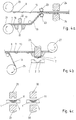
- the identity card 1 shows, in an exemplary embodiment of a data carrier, an identification card 1 with a built-in carrier element 11, on the surface of which the contact surfaces 9 lie.
- the identity card 1 can be made up of a single layer or also of several layers.
- FIG. 2 shows a sectional view of a section of a hot-melt adhesive tape 17 connected to the carrier film 8.
- the carrier film 8 serves to hold the IC chips 5 in a regular arrangement.
- the IC module 5 is connected in a recess 13 in the carrier film 8 directly to a conductive layer 15, for example with the aid of an adhesive.
- the desired contact design with the contact surfaces 9 can be etched out of the conductive layer 15.
- the cutouts 12 in the carrier film 8 allow access to the contact areas 9. In this way, an electrical connection between the connection points of the IC module 5 and the corresponding contact areas 9 can be established in a simple manner.
- the so-called wire bonding technique was used, in which fine gold wires or aluminum wires establish the electrical connection (conductor tracks 14).
- a casting compound 10 is applied to the side of the carrier film 8 opposite the contact surfaces 9 and is of such a size that the IC component 5, the conductor tracks 14 and the connection points between the conductor tracks 14 and the contact surfaces 9 in the recesses 12 of the casting compound 10 are included.
- a hardening resin can be used as casting compound 10.
- the hot adhesive tape 17 arranged on the second side of the carrier film 8 consists of a carrier tape 16 with a hot adhesive layer 7 located thereon and is firmly connected to the carrier film 8 by means of this.
- the hot-melt adhesive tape 17 is provided with openings 19 at regular intervals.
- the size of the openings 19 in the hot-melt adhesive tape 17 is dimensioned such that the casting compound 10 located on the carrier film 8 is at least partially covered by the hot-melt adhesive tape 17 in the edge region.
- the carrier tape 16 is pulled off before the mounting of the carrier element 11 in an identification card.
- Fig. 3 shows the completed ID card 1 in section along the line AA shown in Fig. 1.
- the correspondingly shaped two-stage recess 3 in the card 1 for the installation of the carrier element 11 has, in its central region, a blind hole 2 for receiving the IC component 10 cast with a casting resin.
- the two-stage recess 3 can, for example, in one with the associated deeper blind hole 2 a plastic plate existing card body are milled.
- the card 1 consists of several layers, for example a core layer and an upper and lower cover layer, the upper cover layer and the core layer are provided with a corresponding opening in order to be able to embed the carrier element with a precise fit.
- the overlap of the casting compound 10 by the adhesive layer 7 also leads to the step edge 6 in the recess 3 being covered by the hot-melt adhesive layer 7. Embossments of this edge 6 on the back of the card 4, which can occur when heat and pressure are required to install the carrier element 11 in the card 1, are minimized or avoided in this way.
- This buffer or protective function is performed by the adhesive layer 7 with respect to the edges 6 even with corresponding mechanical loads in daily use of the card 1.
- the overlap leads to the fact that the casting compound 10 is also connected to the card body 1 via the adhesive layer 7, which is the Connection of the carrier element 11 with the card body 1 is still improved overall.
- the opening 19 in the adhesive layer 7 in the region of the blind hole 2 leads to the fact that the carrier element 11 in the region of the casting compound 10 is not connected to the bottom of the blind hole 2 and that less heat is transferred to the comparatively thin rear wall 4 during the installation of the carrier element 11 Card is transferred. As a result, warping or deformation of the thin rear wall 4 of the card 1 can be avoided.
- the opening 19 in the adhesive layer 7 also leads to the fact that in the region of the blind hole 2 below the casting compound 10, a cavity remains which allows the carrier element 11 to move freely enables. In the case of bending stresses on the card 1, this relieves the stress on the IC module 5.
- the cavity also enables a certain margin of tolerance with respect to the thickness of the molding compound 10 to be allowed.
- FIG. 4a shows the carrier film 8 which is unwound from a roll 20 and has the IC components mounted thereon and subsequently cast with a casting resin 10.
- the openings 19 are punched out of the hot-melt adhesive tape 17 at regular intervals using a corresponding punching tool 22.
- the hot adhesive tape 17 provided with the openings 19 is brought together with the carrier film 8 for further processing by means of corresponding guide rollers 23, the punched openings 19 in the hot adhesive tape 17 being able to be used for clocked transport.
- the casting compounds 10 provided on the carrier film 8 in accordance with the arrangement of the IC components are at least partially covered by the hot-melt adhesive tape 17.
- the hot adhesive tape 17 can be connected to the carrier film 8 under the action of heat and pressure with the aid of a heat seal stamp 24.
- a plurality of heat seal stamps 24 can also be used, which then operate in parallel with the same cycle.
- the laminate, consisting of the carrier film 8 and the hot adhesive tape 17, can be wound up on a roll, not shown, for storage. The laminate can also be fed directly to the following process steps.
- 4b shows a punching tool 26 with which the carrier elements 11 are punched out of the laminate together with the hot-melt adhesive layer 7 from the carrier film 8 or from the hot-melt adhesive tape 17.
- the carrier tape 16 is pulled off before the punching process and wound on the roll 25.
- the carrier element 11 underlaid with the hot-melt adhesive layer 7 can also be held by the punching tool 26 and installed in the card body 1 provided with a two-stage recess 3.
- the grid remaining after the carrier elements 11 and the hot-melt adhesive layers 7 have been punched out are wound up on the roll 27.
- the opening in the hot-melt adhesive tape is punched out circularly.
- other contours are possible.
- FIG. 5 shows a hot-melt adhesive tape 17 from which elements 31 are punched out along the dashed lines, as described above.
- a circular opening 33 is punched with a channel 32 which leads from the opening 33 to the punched edge of the element 31 indicated by dashed lines.
- a hermetic seal of the cavity remaining in the blind hole 2 of the card 1 is avoided by the channel 32. Any overpressure that may arise in this cavity under the influence of heat, which can put stress on the card and module, is compensated for via the channel.
- the channel 32 can be dimensioned in such a way that even in the finished card, an opening remains which connects the cavity with the surroundings of the card
Applications Claiming Priority (2)
| Application Number | Priority Date | Filing Date | Title |
|---|---|---|---|
| DE4040770 | 1990-12-19 | ||
| DE4040770A DE4040770C2 (de) | 1990-12-19 | 1990-12-19 | Datenträger mit integriertem Schaltkreis |
Publications (2)
| Publication Number | Publication Date |
|---|---|
| EP0493738A1 true EP0493738A1 (fr) | 1992-07-08 |
| EP0493738B1 EP0493738B1 (fr) | 1997-07-09 |
Family
ID=6420778
Family Applications (1)
| Application Number | Title | Priority Date | Filing Date |
|---|---|---|---|
| EP91121612A Expired - Lifetime EP0493738B1 (fr) | 1990-12-19 | 1991-12-17 | Support d'information avec circuit intégré |
Country Status (6)
| Country | Link |
|---|---|
| EP (1) | EP0493738B1 (fr) |
| JP (1) | JP3248932B2 (fr) |
| AT (1) | ATE155270T1 (fr) |
| DE (2) | DE4040770C2 (fr) |
| ES (1) | ES2106048T3 (fr) |
| SG (1) | SG52281A1 (fr) |
Cited By (12)
| Publication number | Priority date | Publication date | Assignee | Title |
|---|---|---|---|---|
| DE4427802C1 (de) * | 1994-08-05 | 1995-10-26 | Beiersdorf Ag | Thermoaktivierbare Klebfolie zur Herstellung eines Datenträgers |
| EP0724228A2 (fr) * | 1995-01-26 | 1996-07-31 | Giesecke & Devrient GmbH | Procédé de montage d'un module électronique dans un corps de carte |
| US5637858A (en) * | 1993-12-23 | 1997-06-10 | Giesecke & Devrient Gmbh | Method for producing identity cards |
| EP0842995A1 (fr) | 1995-05-27 | 1998-05-20 | Beiersdorf Aktiengesellschaft | Adhésif thermoplastique |
| EP0742926B1 (fr) * | 1994-02-04 | 1998-07-08 | Giesecke & Devrient GmbH | Support de donnees a module electronique et son procede de fabrication |
| EP0789323A3 (fr) * | 1996-02-12 | 1999-09-22 | Marconi Communications Limited | Carte à contact |
| WO2001001341A1 (fr) * | 1999-06-29 | 2001-01-04 | Orga Kartensysteme Gmbh | Element support pour module a circuit integre |
| FR2845805A1 (fr) * | 2002-10-10 | 2004-04-16 | Gemplus Card Int | Adhesif d'encartage formant navette |
| KR100480522B1 (ko) * | 1995-08-01 | 2005-08-31 | 오스트리아 카드 플라스틱카르텐 운트 아우스바이스시스템게젤샤프트 엠베하 | 컴포넌트보유모듈및코일을갖는데이터캐리어와이데이터캐리어의제조방법 |
| KR100487175B1 (ko) * | 1995-08-01 | 2005-09-02 | 오스트리아 카드 플라스틱카르텐 운트 아우스바이스시스템게젤샤프트 엠베하 | 전자구성요소를포함하는모듈과코일을가지는데이터캐리어와,그제조방법 |
| WO2022243432A1 (fr) * | 2021-05-21 | 2022-11-24 | Zwipe As | Fabrication d'une carte à puce |
| GB2607113A (en) * | 2021-05-21 | 2022-11-30 | Zwipe As | Manufacturing a smartcard |
Families Citing this family (7)
| Publication number | Priority date | Publication date | Assignee | Title |
|---|---|---|---|---|
| DE4122049A1 (de) * | 1991-07-03 | 1993-01-07 | Gao Ges Automation Org | Verfahren zum einbau eines traegerelements |
| DE4340847A1 (de) * | 1993-11-26 | 1995-06-01 | Optosys Gmbh Berlin | Chipmodul und Verfahren zur Herstellung eines Chipmoduls |
| JPH09315061A (ja) * | 1996-06-03 | 1997-12-09 | Minolta Co Ltd | Icカードおよびicカード装着装置 |
| FR2791035B1 (fr) * | 1999-03-19 | 2001-07-27 | Allibert Equipement | Procede de conditionnement d'une etiquette electronique, etiquette et piece plastique correspondantes |
| ATE261846T1 (de) * | 1999-12-31 | 2004-04-15 | Allibert Equipement | Verfahren zum herstellen eines elektronischen etiketts sowie die korrespondierende chipkarte |
| DE10357837B4 (de) * | 2003-12-09 | 2013-08-08 | Sennheiser Electronic Gmbh & Co. Kg | Verfahren zur Oberflächenmontage von akustischen Wandlern |
| DE102012001346A1 (de) | 2012-01-24 | 2013-07-25 | Giesecke & Devrient Gmbh | Verfahren zum Herstellen eines Datenträgers |
Citations (4)
| Publication number | Priority date | Publication date | Assignee | Title |
|---|---|---|---|---|
| GB2112324A (en) * | 1981-12-24 | 1983-07-20 | Gao Ges Automation Org | An identification card with an ic module |
| DE3248385A1 (de) * | 1982-12-28 | 1984-06-28 | GAO Gesellschaft für Automation und Organisation mbH, 8000 München | Ausweiskarte mit integriertem schaltkreis |
| EP0268830A2 (fr) * | 1986-11-20 | 1988-06-01 | GAO Gesellschaft für Automation und Organisation mbH | Support de données avec circuit intégré et procédé pour sa fabrication |
| EP0201952B1 (fr) * | 1985-04-12 | 1990-09-19 | Philips Composants | Procédé et dispositif pour fabriquer une carte d'identification électronique |
Family Cites Families (3)
| Publication number | Priority date | Publication date | Assignee | Title |
|---|---|---|---|---|
| JPS58116496A (ja) * | 1981-12-29 | 1983-07-11 | Nippon Kayaku Co Ltd | アミドn置換ブレオマイシン類 |
| DE3723547C2 (de) * | 1987-07-16 | 1996-09-26 | Gao Ges Automation Org | Trägerelement zum Einbau in Ausweiskarten |
| FR2629236B1 (fr) * | 1988-03-22 | 1991-09-27 | Schlumberger Ind Sa | Procede de realisation d'une carte a memoire electronique et carte telle qu'obtenue par la mise en oeuvre dudit procede |
-
1990
- 1990-12-19 DE DE4040770A patent/DE4040770C2/de not_active Expired - Fee Related
-
1991
- 1991-12-16 JP JP33221091A patent/JP3248932B2/ja not_active Expired - Fee Related
- 1991-12-17 SG SG1996001953A patent/SG52281A1/en unknown
- 1991-12-17 DE DE59108771T patent/DE59108771D1/de not_active Expired - Lifetime
- 1991-12-17 EP EP91121612A patent/EP0493738B1/fr not_active Expired - Lifetime
- 1991-12-17 AT AT91121612T patent/ATE155270T1/de not_active IP Right Cessation
- 1991-12-17 ES ES91121612T patent/ES2106048T3/es not_active Expired - Lifetime
Patent Citations (4)
| Publication number | Priority date | Publication date | Assignee | Title |
|---|---|---|---|---|
| GB2112324A (en) * | 1981-12-24 | 1983-07-20 | Gao Ges Automation Org | An identification card with an ic module |
| DE3248385A1 (de) * | 1982-12-28 | 1984-06-28 | GAO Gesellschaft für Automation und Organisation mbH, 8000 München | Ausweiskarte mit integriertem schaltkreis |
| EP0201952B1 (fr) * | 1985-04-12 | 1990-09-19 | Philips Composants | Procédé et dispositif pour fabriquer une carte d'identification électronique |
| EP0268830A2 (fr) * | 1986-11-20 | 1988-06-01 | GAO Gesellschaft für Automation und Organisation mbH | Support de données avec circuit intégré et procédé pour sa fabrication |
Cited By (15)
| Publication number | Priority date | Publication date | Assignee | Title |
|---|---|---|---|---|
| US5637858A (en) * | 1993-12-23 | 1997-06-10 | Giesecke & Devrient Gmbh | Method for producing identity cards |
| EP0742926B1 (fr) * | 1994-02-04 | 1998-07-08 | Giesecke & Devrient GmbH | Support de donnees a module electronique et son procede de fabrication |
| US5888624A (en) * | 1994-02-04 | 1999-03-30 | Giesecke & Devrient Gmbh | Data carrier with an electronic module and a method for producing the same |
| DE4427802C1 (de) * | 1994-08-05 | 1995-10-26 | Beiersdorf Ag | Thermoaktivierbare Klebfolie zur Herstellung eines Datenträgers |
| EP0724228A3 (fr) * | 1995-01-26 | 1998-01-07 | Giesecke & Devrient GmbH | Procédé de montage d'un module électronique dans un corps de carte |
| EP0724228A2 (fr) * | 1995-01-26 | 1996-07-31 | Giesecke & Devrient GmbH | Procédé de montage d'un module électronique dans un corps de carte |
| US5951810A (en) * | 1995-01-26 | 1999-09-14 | Giesecke & Devrient Gmbh | Method for mounting an electronic module in a card body |
| EP0842995A1 (fr) | 1995-05-27 | 1998-05-20 | Beiersdorf Aktiengesellschaft | Adhésif thermoplastique |
| KR100480522B1 (ko) * | 1995-08-01 | 2005-08-31 | 오스트리아 카드 플라스틱카르텐 운트 아우스바이스시스템게젤샤프트 엠베하 | 컴포넌트보유모듈및코일을갖는데이터캐리어와이데이터캐리어의제조방법 |
| KR100487175B1 (ko) * | 1995-08-01 | 2005-09-02 | 오스트리아 카드 플라스틱카르텐 운트 아우스바이스시스템게젤샤프트 엠베하 | 전자구성요소를포함하는모듈과코일을가지는데이터캐리어와,그제조방법 |
| EP0789323A3 (fr) * | 1996-02-12 | 1999-09-22 | Marconi Communications Limited | Carte à contact |
| WO2001001341A1 (fr) * | 1999-06-29 | 2001-01-04 | Orga Kartensysteme Gmbh | Element support pour module a circuit integre |
| FR2845805A1 (fr) * | 2002-10-10 | 2004-04-16 | Gemplus Card Int | Adhesif d'encartage formant navette |
| WO2022243432A1 (fr) * | 2021-05-21 | 2022-11-24 | Zwipe As | Fabrication d'une carte à puce |
| GB2607113A (en) * | 2021-05-21 | 2022-11-30 | Zwipe As | Manufacturing a smartcard |
Also Published As
| Publication number | Publication date |
|---|---|
| DE4040770C2 (de) | 1999-11-11 |
| SG52281A1 (en) | 1998-09-28 |
| ES2106048T3 (es) | 1997-11-01 |
| JP3248932B2 (ja) | 2002-01-21 |
| EP0493738B1 (fr) | 1997-07-09 |
| ATE155270T1 (de) | 1997-07-15 |
| DE4040770A1 (de) | 1992-06-25 |
| DE59108771D1 (de) | 1997-08-14 |
| JPH04314598A (ja) | 1992-11-05 |
Similar Documents
| Publication | Publication Date | Title |
|---|---|---|
| EP0493738B1 (fr) | Support d'information avec circuit intégré | |
| EP0554916B1 (fr) | Module de circuit intégré | |
| EP0723245B1 (fr) | Produit semi-fini à module électronique | |
| EP0140230B1 (fr) | Support d'enregistrement portant un circuit intégré et procédé de production | |
| DE102005058101B4 (de) | Chipkarte und Verfahren zur Herstellung einer Chipkarte | |
| EP1271399B1 (fr) | Porteur de données avec circuit intégré | |
| DE3153769C2 (de) | Trägerelement zum Einbau in Ausweiskarten | |
| EP2260683B1 (fr) | Procédé de fabrication d'un module électronique | |
| DE102004011702B4 (de) | Verfahren zur Herstellung eines Kartenkörpers für eine kontaktlose Chipkarte | |
| EP0521502B1 (fr) | Procédé pour l'installation d'un support | |
| EP0869453A2 (fr) | Procédé de fabrication de carte à puce | |
| WO1997005569A1 (fr) | Support de donnees comportant un module pourvu d'un composant et d'une bobine, et procede de fabrication dudit support de donnees | |
| EP0842493B1 (fr) | Support de donnees muni d'un module comportant un composant et d'une bobine, procede de production d'un support de donnees de ce type et module approprie | |
| DE69824679T2 (de) | Kontaktlose elektronische Karte und Verfahren zur Herstellung einer solchen Karte | |
| EP0843358A2 (fr) | Module électronique à type mince et carte à puce | |
| DE19651566A1 (de) | Chip-Modul sowie Verfahren zu dessen Herstellung | |
| EP0842492A1 (fr) | Support de donnees sous forme de carte pour applications sans contact, comportant un composant et un systeme de transmission pour applications sans contact, procede permettant de produire un support de donnees sous forme de carte de ce type et module approprie | |
| EP0791446B1 (fr) | Procédé et moule d'injection de matières plastiques pour la fabrication d'un article composite | |
| DE19532755C1 (de) | Chipmodul, insbesondere für den Einbau in Chipkarten, und Verfahren zur Herstellung eines derartigen Chipmoduls | |
| DE69929981T2 (de) | Verfahren zum herstellen einer kontaktlosen chipkarte | |
| DE602004004647T2 (de) | Verfahren zum zusammenbauen eines elektronischen komponent auf einem substrat | |
| DE10236666A1 (de) | Verfahren zum Herstellen von Kontaktlosen und/oder gemischten Chipkarten | |
| EP0569417B1 (fr) | Procede pour fabriquer un support de donnees portable | |
| EP1436777B1 (fr) | Procede de production d'un support de donnees et support de donnees produit selon ce procede | |
| DE19918852C1 (de) | Chipkarte mit Flip-Chip und Verfahren zu ihrer Herstellung |
Legal Events
| Date | Code | Title | Description |
|---|---|---|---|
| PUAI | Public reference made under article 153(3) epc to a published international application that has entered the european phase |
Free format text: ORIGINAL CODE: 0009012 |
|
| AK | Designated contracting states |
Kind code of ref document: A1 Designated state(s): AT BE CH DE ES FR GB IT LI LU NL SE |
|
| 17P | Request for examination filed |
Effective date: 19921216 |
|
| 17Q | First examination report despatched |
Effective date: 19950906 |
|
| GRAG | Despatch of communication of intention to grant |
Free format text: ORIGINAL CODE: EPIDOS AGRA |
|
| GRAH | Despatch of communication of intention to grant a patent |
Free format text: ORIGINAL CODE: EPIDOS IGRA |
|
| GRAH | Despatch of communication of intention to grant a patent |
Free format text: ORIGINAL CODE: EPIDOS IGRA |
|
| GRAA | (expected) grant |
Free format text: ORIGINAL CODE: 0009210 |
|
| AK | Designated contracting states |
Kind code of ref document: B1 Designated state(s): AT BE CH DE ES FR GB IT LI LU NL SE |
|
| REF | Corresponds to: |
Ref document number: 155270 Country of ref document: AT Date of ref document: 19970715 Kind code of ref document: T |
|
| RIN1 | Information on inventor provided before grant (corrected) |
Inventor name: BARAK, RENEE-LUCIA Inventor name: HAGHIRI, YAHYA |
|
| REG | Reference to a national code |
Ref country code: CH Ref legal event code: EP |
|
| REF | Corresponds to: |
Ref document number: 59108771 Country of ref document: DE Date of ref document: 19970814 |
|
| ITF | It: translation for a ep patent filed |
Owner name: STUDIO ING. ALFREDO RAIMONDI |
|
| REG | Reference to a national code |
Ref country code: CH Ref legal event code: NV Representative=s name: PATENTANWAELTE SCHAAD, BALASS, MENZL & PARTNER AG |
|
| ET | Fr: translation filed | ||
| GBT | Gb: translation of ep patent filed (gb section 77(6)(a)/1977) |
Effective date: 19971002 |
|
| REG | Reference to a national code |
Ref country code: ES Ref legal event code: FG2A Ref document number: 2106048 Country of ref document: ES Kind code of ref document: T3 |
|
| PG25 | Lapsed in a contracting state [announced via postgrant information from national office to epo] |
Ref country code: LU Free format text: LAPSE BECAUSE OF NON-PAYMENT OF DUE FEES Effective date: 19971217 |
|
| PLBI | Opposition filed |
Free format text: ORIGINAL CODE: 0009260 |
|
| PLBF | Reply of patent proprietor to notice(s) of opposition |
Free format text: ORIGINAL CODE: EPIDOS OBSO |
|
| PLAB | Opposition data, opponent's data or that of the opponent's representative modified |
Free format text: ORIGINAL CODE: 0009299OPPO |
|
| 26 | Opposition filed |
Opponent name: SOCIETE GEMPLUS CARD INTERNATIONAL Effective date: 19980407 |
|
| R26 | Opposition filed (corrected) |
Opponent name: GEMPLUS Effective date: 19980407 |
|
| NLR1 | Nl: opposition has been filed with the epo |
Opponent name: SOCIETE GEMPLUS CARD INTERNATIONAL |
|
| NLR1 | Nl: opposition has been filed with the epo |
Opponent name: GEMPLUS |
|
| PLBF | Reply of patent proprietor to notice(s) of opposition |
Free format text: ORIGINAL CODE: EPIDOS OBSO |
|
| TPAD | Observations filed by third parties |
Free format text: ORIGINAL CODE: EPIDOS TIPA |
|
| PLBO | Opposition rejected |
Free format text: ORIGINAL CODE: EPIDOS REJO |
|
| APAC | Appeal dossier modified |
Free format text: ORIGINAL CODE: EPIDOS NOAPO |
|
| APAE | Appeal reference modified |
Free format text: ORIGINAL CODE: EPIDOS REFNO |
|
| APAC | Appeal dossier modified |
Free format text: ORIGINAL CODE: EPIDOS NOAPO |
|
| REG | Reference to a national code |
Ref country code: GB Ref legal event code: IF02 |
|
| PGFP | Annual fee paid to national office [announced via postgrant information from national office to epo] |
Ref country code: BE Payment date: 20030107 Year of fee payment: 12 |
|
| APCC | Communication from the board of appeal sent |
Free format text: ORIGINAL CODE: EPIDOS OBAPO |
|
| APCA | Receipt of observations in appeal recorded |
Free format text: ORIGINAL CODE: EPIDOSNOBA4O |
|
| RAP2 | Party data changed (patent owner data changed or rights of a patent transferred) |
Owner name: GIESECKE & DEVRIENT GMBH |
|
| NLT2 | Nl: modifications (of names), taken from the european patent patent bulletin |
Owner name: GIESECKE & DEVRIENT GMBH |
|
| PG25 | Lapsed in a contracting state [announced via postgrant information from national office to epo] |
Ref country code: BE Free format text: LAPSE BECAUSE OF NON-PAYMENT OF DUE FEES Effective date: 20031231 |
|
| APBU | Appeal procedure closed |
Free format text: ORIGINAL CODE: EPIDOSNNOA9O |
|
| PLBN | Opposition rejected |
Free format text: ORIGINAL CODE: 0009273 |
|
| STAA | Information on the status of an ep patent application or granted ep patent |
Free format text: STATUS: OPPOSITION REJECTED |
|
| 27O | Opposition rejected |
Effective date: 20040307 |
|
| BERE | Be: lapsed |
Owner name: G.- FUR AUTOMATION UND ORGANISATION M.B.H. *GAO Effective date: 20031231 |
|
| NLR2 | Nl: decision of opposition |
Effective date: 20040307 |
|
| APAH | Appeal reference modified |
Free format text: ORIGINAL CODE: EPIDOSCREFNO |
|
| PGFP | Annual fee paid to national office [announced via postgrant information from national office to epo] |
Ref country code: SE Payment date: 20051222 Year of fee payment: 15 |
|
| PG25 | Lapsed in a contracting state [announced via postgrant information from national office to epo] |
Ref country code: SE Free format text: LAPSE BECAUSE OF NON-PAYMENT OF DUE FEES Effective date: 20061218 |
|
| EUG | Se: european patent has lapsed | ||
| PGFP | Annual fee paid to national office [announced via postgrant information from national office to epo] |
Ref country code: NL Payment date: 20071213 Year of fee payment: 17 |
|
| NLV4 | Nl: lapsed or anulled due to non-payment of the annual fee |
Effective date: 20090701 |
|
| PG25 | Lapsed in a contracting state [announced via postgrant information from national office to epo] |
Ref country code: NL Free format text: LAPSE BECAUSE OF NON-PAYMENT OF DUE FEES Effective date: 20090701 |
|
| PGFP | Annual fee paid to national office [announced via postgrant information from national office to epo] |
Ref country code: AT Payment date: 20101220 Year of fee payment: 20 Ref country code: FR Payment date: 20110107 Year of fee payment: 20 |
|
| PGFP | Annual fee paid to national office [announced via postgrant information from national office to epo] |
Ref country code: CH Payment date: 20101223 Year of fee payment: 20 |
|
| PGFP | Annual fee paid to national office [announced via postgrant information from national office to epo] |
Ref country code: GB Payment date: 20101221 Year of fee payment: 20 |
|
| PGFP | Annual fee paid to national office [announced via postgrant information from national office to epo] |
Ref country code: IT Payment date: 20101229 Year of fee payment: 20 Ref country code: DE Payment date: 20110225 Year of fee payment: 20 |
|
| PGFP | Annual fee paid to national office [announced via postgrant information from national office to epo] |
Ref country code: ES Payment date: 20101222 Year of fee payment: 20 |
|
| REG | Reference to a national code |
Ref country code: DE Ref legal event code: R071 Ref document number: 59108771 Country of ref document: DE |
|
| REG | Reference to a national code |
Ref country code: DE Ref legal event code: R071 Ref document number: 59108771 Country of ref document: DE |
|
| REG | Reference to a national code |
Ref country code: CH Ref legal event code: PL |
|
| REG | Reference to a national code |
Ref country code: GB Ref legal event code: PE20 Expiry date: 20111216 |
|
| PG25 | Lapsed in a contracting state [announced via postgrant information from national office to epo] |
Ref country code: GB Free format text: LAPSE BECAUSE OF EXPIRATION OF PROTECTION Effective date: 20111216 |
|
| REG | Reference to a national code |
Ref country code: ES Ref legal event code: FD2A Effective date: 20120305 |
|
| REG | Reference to a national code |
Ref country code: AT Ref legal event code: MK07 Ref document number: 155270 Country of ref document: AT Kind code of ref document: T Effective date: 20111217 |
|
| PG25 | Lapsed in a contracting state [announced via postgrant information from national office to epo] |
Ref country code: ES Free format text: LAPSE BECAUSE OF EXPIRATION OF PROTECTION Effective date: 20111218 |
|
| PG25 | Lapsed in a contracting state [announced via postgrant information from national office to epo] |
Ref country code: DE Free format text: LAPSE BECAUSE OF EXPIRATION OF PROTECTION Effective date: 20111218 |