EP0493738A1 - Record carrier with integrated circuit - Google Patents
Record carrier with integrated circuit Download PDFInfo
- Publication number
- EP0493738A1 EP0493738A1 EP91121612A EP91121612A EP0493738A1 EP 0493738 A1 EP0493738 A1 EP 0493738A1 EP 91121612 A EP91121612 A EP 91121612A EP 91121612 A EP91121612 A EP 91121612A EP 0493738 A1 EP0493738 A1 EP 0493738A1
- Authority
- EP
- European Patent Office
- Prior art keywords
- adhesive layer
- carrier
- carrier element
- casting compound
- hot
- Prior art date
- Legal status (The legal status is an assumption and is not a legal conclusion. Google has not performed a legal analysis and makes no representation as to the accuracy of the status listed.)
- Granted
Links
- 238000005266 casting Methods 0.000 claims abstract description 40
- 239000012790 adhesive layer Substances 0.000 claims abstract description 36
- 150000001875 compounds Chemical class 0.000 claims abstract description 28
- 239000000758 substrate Substances 0.000 claims abstract description 12
- 238000004519 manufacturing process Methods 0.000 claims abstract description 7
- 239000000969 carrier Substances 0.000 claims abstract description 4
- 239000004831 Hot glue Substances 0.000 claims description 27
- 239000010410 layer Substances 0.000 claims description 24
- 239000004822 Hot adhesive Substances 0.000 claims description 13
- 239000004020 conductor Substances 0.000 claims description 11
- 238000000034 method Methods 0.000 claims description 11
- 238000004080 punching Methods 0.000 claims description 8
- 239000000109 continuous material Substances 0.000 claims description 5
- 230000004913 activation Effects 0.000 claims 1
- 239000002390 adhesive tape Substances 0.000 claims 1
- 239000002131 composite material Substances 0.000 claims 1
- 230000002093 peripheral effect Effects 0.000 claims 1
- 229920005989 resin Polymers 0.000 abstract description 5
- 239000011347 resin Substances 0.000 abstract description 5
- 229940125773 compound 10 Drugs 0.000 description 11
- ZLVXBBHTMQJRSX-VMGNSXQWSA-N jdtic Chemical compound C1([C@]2(C)CCN(C[C@@H]2C)C[C@H](C(C)C)NC(=O)[C@@H]2NCC3=CC(O)=CC=C3C2)=CC=CC(O)=C1 ZLVXBBHTMQJRSX-VMGNSXQWSA-N 0.000 description 11
- 239000000853 adhesive Substances 0.000 description 7
- 230000001070 adhesive effect Effects 0.000 description 7
- 238000005452 bending Methods 0.000 description 5
- 238000004026 adhesive bonding Methods 0.000 description 3
- 239000002313 adhesive film Substances 0.000 description 3
- 238000009434 installation Methods 0.000 description 3
- 239000000463 material Substances 0.000 description 3
- 238000001816 cooling Methods 0.000 description 2
- 239000012792 core layer Substances 0.000 description 2
- 239000003822 epoxy resin Substances 0.000 description 2
- 230000006870 function Effects 0.000 description 2
- 229920000647 polyepoxide Polymers 0.000 description 2
- XAGFODPZIPBFFR-UHFFFAOYSA-N aluminium Chemical compound [Al] XAGFODPZIPBFFR-UHFFFAOYSA-N 0.000 description 1
- 229910052782 aluminium Inorganic materials 0.000 description 1
- 238000004891 communication Methods 0.000 description 1
- 238000013461 design Methods 0.000 description 1
- 238000011161 development Methods 0.000 description 1
- 230000018109 developmental process Effects 0.000 description 1
- 239000003292 glue Substances 0.000 description 1
- PCHJSUWPFVWCPO-UHFFFAOYSA-N gold Chemical compound [Au] PCHJSUWPFVWCPO-UHFFFAOYSA-N 0.000 description 1
- 239000010931 gold Substances 0.000 description 1
- 229910052737 gold Inorganic materials 0.000 description 1
- 238000000465 moulding Methods 0.000 description 1
- 239000004033 plastic Substances 0.000 description 1
- 238000012545 processing Methods 0.000 description 1
- 230000009993 protective function Effects 0.000 description 1
- 239000002356 single layer Substances 0.000 description 1
- 238000003860 storage Methods 0.000 description 1
Images


Classifications
-
- G—PHYSICS
- G06—COMPUTING; CALCULATING OR COUNTING
- G06K—GRAPHICAL DATA READING; PRESENTATION OF DATA; RECORD CARRIERS; HANDLING RECORD CARRIERS
- G06K19/00—Record carriers for use with machines and with at least a part designed to carry digital markings
- G06K19/06—Record carriers for use with machines and with at least a part designed to carry digital markings characterised by the kind of the digital marking, e.g. shape, nature, code
- G06K19/067—Record carriers with conductive marks, printed circuits or semiconductor circuit elements, e.g. credit or identity cards also with resonating or responding marks without active components
- G06K19/07—Record carriers with conductive marks, printed circuits or semiconductor circuit elements, e.g. credit or identity cards also with resonating or responding marks without active components with integrated circuit chips
- G06K19/077—Constructional details, e.g. mounting of circuits in the carrier
- G06K19/07718—Constructional details, e.g. mounting of circuits in the carrier the record carrier being manufactured in a continuous process, e.g. using endless rolls
-
- G—PHYSICS
- G06—COMPUTING; CALCULATING OR COUNTING
- G06K—GRAPHICAL DATA READING; PRESENTATION OF DATA; RECORD CARRIERS; HANDLING RECORD CARRIERS
- G06K19/00—Record carriers for use with machines and with at least a part designed to carry digital markings
- G06K19/06—Record carriers for use with machines and with at least a part designed to carry digital markings characterised by the kind of the digital marking, e.g. shape, nature, code
- G06K19/067—Record carriers with conductive marks, printed circuits or semiconductor circuit elements, e.g. credit or identity cards also with resonating or responding marks without active components
- G06K19/07—Record carriers with conductive marks, printed circuits or semiconductor circuit elements, e.g. credit or identity cards also with resonating or responding marks without active components with integrated circuit chips
- G06K19/077—Constructional details, e.g. mounting of circuits in the carrier
- G06K19/07745—Mounting details of integrated circuit chips
-
- H—ELECTRICITY
- H01—ELECTRIC ELEMENTS
- H01L—SEMICONDUCTOR DEVICES NOT COVERED BY CLASS H10
- H01L2224/00—Indexing scheme for arrangements for connecting or disconnecting semiconductor or solid-state bodies and methods related thereto as covered by H01L24/00
- H01L2224/01—Means for bonding being attached to, or being formed on, the surface to be connected, e.g. chip-to-package, die-attach, "first-level" interconnects; Manufacturing methods related thereto
- H01L2224/42—Wire connectors; Manufacturing methods related thereto
- H01L2224/44—Structure, shape, material or disposition of the wire connectors prior to the connecting process
- H01L2224/45—Structure, shape, material or disposition of the wire connectors prior to the connecting process of an individual wire connector
- H01L2224/45001—Core members of the connector
- H01L2224/45099—Material
- H01L2224/451—Material with a principal constituent of the material being a metal or a metalloid, e.g. boron (B), silicon (Si), germanium (Ge), arsenic (As), antimony (Sb), tellurium (Te) and polonium (Po), and alloys thereof
- H01L2224/45117—Material with a principal constituent of the material being a metal or a metalloid, e.g. boron (B), silicon (Si), germanium (Ge), arsenic (As), antimony (Sb), tellurium (Te) and polonium (Po), and alloys thereof the principal constituent melting at a temperature of greater than or equal to 400°C and less than 950°C
- H01L2224/45124—Aluminium (Al) as principal constituent
-
- H—ELECTRICITY
- H01—ELECTRIC ELEMENTS
- H01L—SEMICONDUCTOR DEVICES NOT COVERED BY CLASS H10
- H01L2224/00—Indexing scheme for arrangements for connecting or disconnecting semiconductor or solid-state bodies and methods related thereto as covered by H01L24/00
- H01L2224/01—Means for bonding being attached to, or being formed on, the surface to be connected, e.g. chip-to-package, die-attach, "first-level" interconnects; Manufacturing methods related thereto
- H01L2224/42—Wire connectors; Manufacturing methods related thereto
- H01L2224/44—Structure, shape, material or disposition of the wire connectors prior to the connecting process
- H01L2224/45—Structure, shape, material or disposition of the wire connectors prior to the connecting process of an individual wire connector
- H01L2224/45001—Core members of the connector
- H01L2224/45099—Material
- H01L2224/451—Material with a principal constituent of the material being a metal or a metalloid, e.g. boron (B), silicon (Si), germanium (Ge), arsenic (As), antimony (Sb), tellurium (Te) and polonium (Po), and alloys thereof
- H01L2224/45138—Material with a principal constituent of the material being a metal or a metalloid, e.g. boron (B), silicon (Si), germanium (Ge), arsenic (As), antimony (Sb), tellurium (Te) and polonium (Po), and alloys thereof the principal constituent melting at a temperature of greater than or equal to 950°C and less than 1550°C
- H01L2224/45144—Gold (Au) as principal constituent
-
- H—ELECTRICITY
- H01—ELECTRIC ELEMENTS
- H01L—SEMICONDUCTOR DEVICES NOT COVERED BY CLASS H10
- H01L2224/00—Indexing scheme for arrangements for connecting or disconnecting semiconductor or solid-state bodies and methods related thereto as covered by H01L24/00
- H01L2224/01—Means for bonding being attached to, or being formed on, the surface to be connected, e.g. chip-to-package, die-attach, "first-level" interconnects; Manufacturing methods related thereto
- H01L2224/42—Wire connectors; Manufacturing methods related thereto
- H01L2224/47—Structure, shape, material or disposition of the wire connectors after the connecting process
- H01L2224/48—Structure, shape, material or disposition of the wire connectors after the connecting process of an individual wire connector
- H01L2224/4805—Shape
- H01L2224/4809—Loop shape
- H01L2224/48091—Arched
-
- H—ELECTRICITY
- H01—ELECTRIC ELEMENTS
- H01L—SEMICONDUCTOR DEVICES NOT COVERED BY CLASS H10
- H01L2924/00—Indexing scheme for arrangements or methods for connecting or disconnecting semiconductor or solid-state bodies as covered by H01L24/00
- H01L2924/01—Chemical elements
- H01L2924/01079—Gold [Au]
Definitions
- the invention relates to a data carrier with an integrated circuit according to the preamble of claim 1 and a method for producing such a data carrier.
- Data carriers with an integrated circuit are used, for example, as identification, credit or booking cards or the like.
- One way of producing such cards is to glue a so-called module or carrier element into a correspondingly adapted recess in the card body.
- the modules or carrier elements which are preferably punched out on an endless film, generally consist of a substrate on which one or more integrated circuits are connected to conductor tracks.
- the conductor tracks lead to contact areas located on the substrate, which enable communication with corresponding devices.
- the IC module and the conductor tracks leading from the IC module to the contact areas are preferably surrounded by a casting compound. Many methods for connecting the module to the card body have already become known.
- the hot-melt adhesive layer has a double function. It serves not only to connect the carrier element to the card, but also to form a boundary frame for the casting compound.
- an adhesive layer is applied to the substrate prepared with the IC component, the conductor tracks and the contact areas, which has a cutout in the area of the IC component.
- the area formed by the recess is then filled with a casting compound, the metering of the compound in this way it is set that the IC module is completely enclosed, but the adhesive layer, which limits the casting compound, remains completely free.
- a thermally activated adhesive layer for connecting a carrier element to a card body is also known from EP-A 0 334 733.
- a two-stage recess is provided in the card body.
- a first recess serves to receive the substrate, while a second, deeper recess arranged within the first is provided for receiving the integrated circuit.
- the carrier element is glued to the card body on the shoulder area of the deeper recess.
- a ring-shaped hot-melt adhesive film used for gluing is inserted into the recess beforehand. After inserting the carrier element, it is connected to the card body using heat and pressure.
- the adhesive ring is punched independently of the carrier element and inserted in advance into the recess in the card, all tolerances in the dimensions of the recess in the adhesive ring and the carrier element have an influence on the position of the carrier element and the adhesive ring in the recess, that is to say, as a rule, not the entire available adhesive surface is used, which inevitably results in a lower strength in the connection between the carrier element and the card.
- an epoxy resin drop located on the bottom of the blind hole of the recess also connects to the IC module.
- This measure is intended to ensure that the cured resin improves the mechanical resistance of the bottom area of the recess.
- the measure seems to have the disadvantage, however, that the IC module with a corresponding Bending stress of the card in the bottom area of the blind hole is exposed to strong mechanical punctual stress due to the stiffening of the hardened epoxy resin.
- the bond between the carrier element and the card body produced by the hot-melt adhesive layer is subjected to greater stress in the case of bending loads due to the stiffening in the bottom region of the blind hole. This can lead to the detachment of the adhesive layer on the carrier element or on the card.
- the invention has for its object to achieve a very good and permanent connection when bonding a carrier element in data carriers with the aid of a thermally activated hot-melt adhesive layer while at the same time providing good protection for the integrated circuit against mechanical loads.
- an endless film is assumed, on which integrated circuits are mounted and provided with a casting compound.
- This continuous film is brought together with a thermally activated adhesive film.
- the adhesive film has openings which are dimensioned and positioned in relation to the carrier film in such a way that the adhesive layer at least partially covers not only the carrier film but also the casting compound in the edge regions.
- the carrier elements are punched out of the continuous material together with the adhesive layer.
- the carrier element thus provided with an adhesive layer is connected to the card material in a two-stage recess in a data carrier using heat and pressure.
- the available adhesive surface in the recess is fully utilized regardless of tolerances in any case.
- Man achieves a uniform, large-area and permanent connection between the carrier element and the card body.
- a cavity remains between the casting compound of the carrier element on the one hand and the bottom region of the blind hole of the recess on the other.
- the IC module with the casting compound has a certain freedom of movement even when the card body is subjected to corresponding bending stresses, as a result of which the IC module is relieved of stress when the card is subjected to bending stress. Pressure loads in the area of the carrier elements are not transferred directly to the IC module.
- the thermal load on the card material in the bottom area during the installation of the carrier element is very low. It has been shown that, because of this, the back of the card surface opposite the carrier element has no warpage or deformation in the region of the base. This is particularly important if, for example, the back of the card is to be printed, for which purpose a particularly flat surface is desirable.
- the carrier element is always connected to the card body in the edge region of the cast body via the adhesive layer, as a result of which the adhesion between the carrier element and the card body can be improved overall.
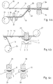
- the identity card 1 shows, in an exemplary embodiment of a data carrier, an identification card 1 with a built-in carrier element 11, on the surface of which the contact surfaces 9 lie.
- the identity card 1 can be made up of a single layer or also of several layers.
- FIG. 2 shows a sectional view of a section of a hot-melt adhesive tape 17 connected to the carrier film 8.
- the carrier film 8 serves to hold the IC chips 5 in a regular arrangement.
- the IC module 5 is connected in a recess 13 in the carrier film 8 directly to a conductive layer 15, for example with the aid of an adhesive.
- the desired contact design with the contact surfaces 9 can be etched out of the conductive layer 15.
- the cutouts 12 in the carrier film 8 allow access to the contact areas 9. In this way, an electrical connection between the connection points of the IC module 5 and the corresponding contact areas 9 can be established in a simple manner.
- the so-called wire bonding technique was used, in which fine gold wires or aluminum wires establish the electrical connection (conductor tracks 14).
- a casting compound 10 is applied to the side of the carrier film 8 opposite the contact surfaces 9 and is of such a size that the IC component 5, the conductor tracks 14 and the connection points between the conductor tracks 14 and the contact surfaces 9 in the recesses 12 of the casting compound 10 are included.
- a hardening resin can be used as casting compound 10.
- the hot adhesive tape 17 arranged on the second side of the carrier film 8 consists of a carrier tape 16 with a hot adhesive layer 7 located thereon and is firmly connected to the carrier film 8 by means of this.
- the hot-melt adhesive tape 17 is provided with openings 19 at regular intervals.
- the size of the openings 19 in the hot-melt adhesive tape 17 is dimensioned such that the casting compound 10 located on the carrier film 8 is at least partially covered by the hot-melt adhesive tape 17 in the edge region.
- the carrier tape 16 is pulled off before the mounting of the carrier element 11 in an identification card.
- Fig. 3 shows the completed ID card 1 in section along the line AA shown in Fig. 1.
- the correspondingly shaped two-stage recess 3 in the card 1 for the installation of the carrier element 11 has, in its central region, a blind hole 2 for receiving the IC component 10 cast with a casting resin.
- the two-stage recess 3 can, for example, in one with the associated deeper blind hole 2 a plastic plate existing card body are milled.
- the card 1 consists of several layers, for example a core layer and an upper and lower cover layer, the upper cover layer and the core layer are provided with a corresponding opening in order to be able to embed the carrier element with a precise fit.
- the overlap of the casting compound 10 by the adhesive layer 7 also leads to the step edge 6 in the recess 3 being covered by the hot-melt adhesive layer 7. Embossments of this edge 6 on the back of the card 4, which can occur when heat and pressure are required to install the carrier element 11 in the card 1, are minimized or avoided in this way.
- This buffer or protective function is performed by the adhesive layer 7 with respect to the edges 6 even with corresponding mechanical loads in daily use of the card 1.
- the overlap leads to the fact that the casting compound 10 is also connected to the card body 1 via the adhesive layer 7, which is the Connection of the carrier element 11 with the card body 1 is still improved overall.
- the opening 19 in the adhesive layer 7 in the region of the blind hole 2 leads to the fact that the carrier element 11 in the region of the casting compound 10 is not connected to the bottom of the blind hole 2 and that less heat is transferred to the comparatively thin rear wall 4 during the installation of the carrier element 11 Card is transferred. As a result, warping or deformation of the thin rear wall 4 of the card 1 can be avoided.
- the opening 19 in the adhesive layer 7 also leads to the fact that in the region of the blind hole 2 below the casting compound 10, a cavity remains which allows the carrier element 11 to move freely enables. In the case of bending stresses on the card 1, this relieves the stress on the IC module 5.
- the cavity also enables a certain margin of tolerance with respect to the thickness of the molding compound 10 to be allowed.
- FIG. 4a shows the carrier film 8 which is unwound from a roll 20 and has the IC components mounted thereon and subsequently cast with a casting resin 10.
- the openings 19 are punched out of the hot-melt adhesive tape 17 at regular intervals using a corresponding punching tool 22.
- the hot adhesive tape 17 provided with the openings 19 is brought together with the carrier film 8 for further processing by means of corresponding guide rollers 23, the punched openings 19 in the hot adhesive tape 17 being able to be used for clocked transport.
- the casting compounds 10 provided on the carrier film 8 in accordance with the arrangement of the IC components are at least partially covered by the hot-melt adhesive tape 17.
- the hot adhesive tape 17 can be connected to the carrier film 8 under the action of heat and pressure with the aid of a heat seal stamp 24.
- a plurality of heat seal stamps 24 can also be used, which then operate in parallel with the same cycle.
- the laminate, consisting of the carrier film 8 and the hot adhesive tape 17, can be wound up on a roll, not shown, for storage. The laminate can also be fed directly to the following process steps.
- 4b shows a punching tool 26 with which the carrier elements 11 are punched out of the laminate together with the hot-melt adhesive layer 7 from the carrier film 8 or from the hot-melt adhesive tape 17.
- the carrier tape 16 is pulled off before the punching process and wound on the roll 25.
- the carrier element 11 underlaid with the hot-melt adhesive layer 7 can also be held by the punching tool 26 and installed in the card body 1 provided with a two-stage recess 3.
- the grid remaining after the carrier elements 11 and the hot-melt adhesive layers 7 have been punched out are wound up on the roll 27.
- the opening in the hot-melt adhesive tape is punched out circularly.
- other contours are possible.
- FIG. 5 shows a hot-melt adhesive tape 17 from which elements 31 are punched out along the dashed lines, as described above.
- a circular opening 33 is punched with a channel 32 which leads from the opening 33 to the punched edge of the element 31 indicated by dashed lines.
- a hermetic seal of the cavity remaining in the blind hole 2 of the card 1 is avoided by the channel 32. Any overpressure that may arise in this cavity under the influence of heat, which can put stress on the card and module, is compensated for via the channel.
- the channel 32 can be dimensioned in such a way that even in the finished card, an opening remains which connects the cavity with the surroundings of the card
Landscapes
- Engineering & Computer Science (AREA)
- Computer Hardware Design (AREA)
- Microelectronics & Electronic Packaging (AREA)
- Physics & Mathematics (AREA)
- General Physics & Mathematics (AREA)
- Theoretical Computer Science (AREA)
- Credit Cards Or The Like (AREA)
- Stabilization Of Oscillater, Synchronisation, Frequency Synthesizers (AREA)
- Structures Or Materials For Encapsulating Or Coating Semiconductor Devices Or Solid State Devices (AREA)
Abstract
Description
Die Erfindung betrifft einen Datenträger mit integriertem Schaltkreis gemäß dem Oberbegriff des Anspruchs 1 sowie ein Verfahren zur Herstellung eines solchen Datenträgers.The invention relates to a data carrier with an integrated circuit according to the preamble of
Datenträger mit integriertem Schaltkreis werden beispielsweise als Identifikations-, Kredit- oder Buchungskarten oder dergleichen eingesetzt. Eine Möglichkeit zur Herstellung solcher Karten besteht darin, ein sogenanntes Modul oder Trägerelement in eine entsprechend angepaßte Aussparung des Kartenkörpers einzukleben. Die Module oder Trägerelemente, die vorzugsweise ans einem Endlosfilm ausgestanzt werden, bestehen im allgemeinen aus einem Substrat, auf dem ein oder mehrere integrierte Schaltkreise mit Leiterbahnen verbunden sind. Die Leiterbahnen führen zu auf dem Substrat befindlichen Kontaktflächen, die die Kommunikation mit entsprechenden Geräten ermöglichen. Vorzugsweise sind der IC-Baustein und die vom IC-Baustein zu den Kontaktflächen führenden Leiterbahnen von einer Gußmasse umgeben. Es sind bereits viele Verfahren bekannt geworden zur Verbindung des Moduls mit dem Kartenkörper.Data carriers with an integrated circuit are used, for example, as identification, credit or booking cards or the like. One way of producing such cards is to glue a so-called module or carrier element into a correspondingly adapted recess in the card body. The modules or carrier elements, which are preferably punched out on an endless film, generally consist of a substrate on which one or more integrated circuits are connected to conductor tracks. The conductor tracks lead to contact areas located on the substrate, which enable communication with corresponding devices. The IC module and the conductor tracks leading from the IC module to the contact areas are preferably surrounded by a casting compound. Many methods for connecting the module to the card body have already become known.
Aus der EP-A 0 299 530 ist es beispielsweise bekannt, das Trägerelement mit Hilfe einer thermoaktivierbaren Klebeschicht in einer angepaßten Aussparung der Karte mit dem Kartenkörper zu verbinden. Bei der bekannten Lösung hat die Heißklebeschicht eine Doppelfunktion. Sie dient nicht nur dazu, das Trägerelement mit der Karte zu verbinden, sondern auch dazu, einen Begrenzungsrahmen für die Gußmasse zu bilden. Dazu wird auf dem mit dem IC-Baustein, den Leiterbahnen und den Kontaktflächen vorbereiteten Substrat eine Klebeschicht aufgebracht, die im Bereich des IC-Bausteins eine Aussparung aufweist. Anschließend wird der durch die Aussparung gebildete Bereich mit einer Gußmasse gefüllt, wobei die Dosierung der Masse derart eingestellt ist, daß der IC-Baustein vollständig eingeschlossen ist, die Klebeschicht aber, die die Gußmasse begrenzt, vollständig frei bleibt.From EP-A 0 299 530 it is known, for example, to connect the carrier element to the card body with the aid of a thermally activated adhesive layer in an adapted recess in the card. In the known solution, the hot-melt adhesive layer has a double function. It serves not only to connect the carrier element to the card, but also to form a boundary frame for the casting compound. For this purpose, an adhesive layer is applied to the substrate prepared with the IC component, the conductor tracks and the contact areas, which has a cutout in the area of the IC component. The area formed by the recess is then filled with a casting compound, the metering of the compound in this way it is set that the IC module is completely enclosed, but the adhesive layer, which limits the casting compound, remains completely free.
Die Verwendung einer thermoaktivierbaren Klebeschicht zur Verbindung eines Trägerelements mit einem Kartenkörper ist auch aus der EP-A 0 334 733 bekannt. Bei dieser bekannten Lösung ist im Kartenkörper eine zweistufige Aussparung vorgesehen. Eine erste Aussparung dient der Aufnahme des Substrats, während eine zweite innerhalb der ersten angeordnete tiefere Aussparung für die Aufnahme des integrierten Schaltkreises vorgesehen ist. Auf dem Schulterbereich der tieferen Aussparung ist das Trägerelement mit dem Kartenkörper verklebt. Ein zur Verklebung eingesetzter, ringförmig gestanzter Heißklebefilm wird vorab in die Aussparung eingesetzt. Nach dem Einsetzen des Trägerlements wird dieses unter Anwendung von Wärme und Druck mit dem Kartenkörper verbunden.The use of a thermally activated adhesive layer for connecting a carrier element to a card body is also known from EP-A 0 334 733. In this known solution, a two-stage recess is provided in the card body. A first recess serves to receive the substrate, while a second, deeper recess arranged within the first is provided for receiving the integrated circuit. The carrier element is glued to the card body on the shoulder area of the deeper recess. A ring-shaped hot-melt adhesive film used for gluing is inserted into the recess beforehand. After inserting the carrier element, it is connected to the card body using heat and pressure.
Da der Klebering unabhängig vom Trägerelement gestanzt und vorab in die Aussparung der Karte eingesetzt wird, haben alle Toleranzen in den Abmaßen der Aussparung des Kleberings und des Trägerelements Einfluß auf die Lage von Trägerelement und Klebering in der Aussparung, das heißt, daß in der Regel nicht die gesamte zur Verfügung stehende Klebefläche genutzt wird, was zwangsläufig eine geringere Festigkeit in der Verbindung zwischen Trägerelement und Karte zur Folge hat.Since the adhesive ring is punched independently of the carrier element and inserted in advance into the recess in the card, all tolerances in the dimensions of the recess in the adhesive ring and the carrier element have an influence on the position of the carrier element and the adhesive ring in the recess, that is to say, as a rule, not the entire available adhesive surface is used, which inevitably results in a lower strength in the connection between the carrier element and the card.
Bei der Verklebung des Trägerelements mit dem Kartenkörper unter Einwirkung von Wärme und Druck verbindet sich auch ein auf dem Boden des Sacklochs der Aussparung befindlicher Epoxydharztropfen mit dem IC-Baustein. Mit dieser Maßnahme soll erreicht werden, daß das ausgehärtete Harz die mechanische Resistenz des Bodenbereichs der Aussparung verbessert. Die Maßnahme scheint aber den Nachteil zu haben, daß der IC-Baustein bei einer entsprechenden Biegebeanspruchung der Karte im Bodenbereich des Sacklochs durch die Versteifung des ausgehärteten Epoxydharzes einer starken mechanischen punktuellen Belastung ausgesetzt ist. Des weiteren wird der durch die Heißklebeschicht hergestellte Verbund zwischen Trägerelement und Kartenkörper bei Biegebelastungen aufgrund der Versteifung im Bodenbereich des Sacklochs stärker beansprucht. Dies kann zur Ablösung der Klebeschicht am Trägerelement oder an der Karte führen.When the carrier element is glued to the card body under the action of heat and pressure, an epoxy resin drop located on the bottom of the blind hole of the recess also connects to the IC module. This measure is intended to ensure that the cured resin improves the mechanical resistance of the bottom area of the recess. The measure seems to have the disadvantage, however, that the IC module with a corresponding Bending stress of the card in the bottom area of the blind hole is exposed to strong mechanical punctual stress due to the stiffening of the hardened epoxy resin. Furthermore, the bond between the carrier element and the card body produced by the hot-melt adhesive layer is subjected to greater stress in the case of bending loads due to the stiffening in the bottom region of the blind hole. This can lead to the detachment of the adhesive layer on the carrier element or on the card.
Der Erfindung liegt die Aufgabe zugrunde, bei einer Verklebung eines Trägerelements in Datenträgern mit Hilfe einer thermoaktivierbaren Heißklebeschicht eine sehr gute und dauerhafte Verbindung zu erzielen bei gleichzeitig gutem Schutz des integrierten Schaltkreises gegen mechanische Belastungen.The invention has for its object to achieve a very good and permanent connection when bonding a carrier element in data carriers with the aid of a thermally activated hot-melt adhesive layer while at the same time providing good protection for the integrated circuit against mechanical loads.
Die Aufgabe wird durch die im kennzeichnenden Teil des Hauptanspruchs angegebenen Merkmale gelöst.The object is achieved by the features specified in the characterizing part of the main claim.
Bei der Erfindung wird von einem Endlosfilm ausgegangen, auf dem integrierte Schaltkreise montiert und mit einer Gußmasse versehen sind. Dieser Endlosfilm wird mit einem thermoaktivierbaren Klebefilm zusammengeführt. Der Klebefilm hat Öffnungen, die derart bemessen und zum Trägerfilm positioniert werden, daß die Klebeschicht nicht nur den Trägerfilm, sondern auch die Gußmasse in den Randbereichen zumindest teilweise überdeckt. Die Trägerelemente werden gemeinsam mit der Klebeschicht aus dem Endlosmaterial gestanzt. Das so mit einer Klebeschicht versehene Trägerelement wird unter Anwendung von Wärme und Druck in einer zweistufigen Aussparung eines Datenträgers mit dem Kartenmaterial verbunden.In the invention, an endless film is assumed, on which integrated circuits are mounted and provided with a casting compound. This continuous film is brought together with a thermally activated adhesive film. The adhesive film has openings which are dimensioned and positioned in relation to the carrier film in such a way that the adhesive layer at least partially covers not only the carrier film but also the casting compound in the edge regions. The carrier elements are punched out of the continuous material together with the adhesive layer. The carrier element thus provided with an adhesive layer is connected to the card material in a two-stage recess in a data carrier using heat and pressure.
Mit der erfindungsgemäßen Lösung wird die zur Verfügung stehende Klebefläche in der Aussparung unabhängig von Toleranzen in jedem Fall vollständig ausgenutzt. Man erzielt damit eine gleichmäßige, großflächige und dauerhafte Verbindung zwischen Trägerelement und Kartenkörper. Aufgrund der Aussparung in der Klebeschicht verbleibt ein Hohlraum zwischen der Gußmasse des Trägerelements einerseits und dem Bodenbereich des Sacklochs der Aussparung andererseits. Durch diesen Hohlraum hat der IC-Baustein mit der Vergußmasse auch bei entsprechenden Biegebeanspruchungen des Kartenkörpers eine gewisse Bewegungsfreiheit, wodurch der IC-Baustein bei Biegebeanspruchungen der Karte entlastet wird. Druckbelastungen im Bereich der Trägerelemente werden nicht direkt auf den IC-Baustein übertragen. Da zwischen dem Gußkörper und dem im allgemeinen sehr dünnen Bodenbereich der Aussparung keine Verbindung hergestellt wird, ist die thermische Belastung des Kartenmaterials im Bodenbereich während des Einbaus des Trägerelements sehr gering. Es hat sich gezeigt, daß aufgrund dessen die dem Trägerelement gegenüberliegende rückseitige Kartenoberfläche im Bereich des Bodens keinerlei Verzüge oder Deformationen aufweist. Dies ist besonders dann von Bedeutung, wenn die Kartenrückseite beispielsweise bedruckt werden soll, wozu eine besonders plane Oberfläche wünschenswert ist.With the solution according to the invention, the available adhesive surface in the recess is fully utilized regardless of tolerances in any case. Man achieves a uniform, large-area and permanent connection between the carrier element and the card body. Because of the recess in the adhesive layer, a cavity remains between the casting compound of the carrier element on the one hand and the bottom region of the blind hole of the recess on the other. As a result of this cavity, the IC module with the casting compound has a certain freedom of movement even when the card body is subjected to corresponding bending stresses, as a result of which the IC module is relieved of stress when the card is subjected to bending stress. Pressure loads in the area of the carrier elements are not transferred directly to the IC module. Since no connection is made between the cast body and the generally very thin bottom area of the recess, the thermal load on the card material in the bottom area during the installation of the carrier element is very low. It has been shown that, because of this, the back of the card surface opposite the carrier element has no warpage or deformation in the region of the base. This is particularly important if, for example, the back of the card is to be printed, for which purpose a particularly flat surface is desirable.
Bei der erfindungsgemäßen Vorgehensweise wird das Trägerelement immer auch im Randbereich des Gußkörpers über die Klebeschicht mit dem Kartenkörper verbunden, wodurch die Haftung zwischen Trägerelement und Kartenkörper insgesamt noch verbessert werden kann.In the procedure according to the invention, the carrier element is always connected to the card body in the edge region of the cast body via the adhesive layer, as a result of which the adhesion between the carrier element and the card body can be improved overall.
Weitere Vorteile und Weiterbildungen der Erfindung ergeben sich aus den Unteransprüchen sowie den Ausführungsbeispielen, die nachfolgend anhand der Figuren beschrieben werden. Darin zeigen:
- Fig. 1
- eine Ausweiskarte mit eingebautem Trägerelement in der Draufsicht,
- Fig. 2
- einen Trägerfilm mit darauf angeordneten IC-Bausteinen und mit einem Heißklebeband im Schnitt,
- Fig. 3
- eine Ausweiskarte mit eingebautem Trägerelement gemäß Fig. 1 im Schnitt,
- Fig. 4a - 4c
- ein Verfahren zur Herstellung einer Ausweiskarte gemäß Fig. 3 und
- Fig. 5
- eine Heißklebeschicht.
- Fig. 1
- an identification card with built-in carrier element in plan view,
- Fig. 2
- a carrier film with IC components arranged on it and with a hot adhesive tape in section,
- Fig. 3
- an ID card with built-in support element according to FIG. 1 in section,
- Figures 4a - 4c
- a method for producing an ID card according to FIG. 3 and
- Fig. 5
- a hot glue layer.
Fig. 1 zeigt in einer beispielhaften Ausführungsform eines Datenträgers eine Ausweiskarte 1 mit eingebautem Trägerelement 11, auf dessen Oberfläche die Kontaktflächen 9 liegen. Die Ausweiskarte 1 kann aus einer einzigen Schicht oder auch aus mehreren Schichten aufgebaut sein.1 shows, in an exemplary embodiment of a data carrier, an
Fig. 2 zeigt in einer Schnittdarstellung einen Ausschnitt eines mit dem Trägerfilm 8 verbundenen Heißklebebandes 17. Der Trägerfilm 8 dient zur Aufnahme der IC-Bausteine 5 in regelmäßiger Anordnung. In dem gezeigten Ausführungsbeispiel ist der IC-Baustein 5 in einer Aussparung 13 des Trägerfilms 8 direkt mit einer leitenden Schicht 15, beispielsweise mit Hilfe eines Klebstoffes, verbunden. Aus der leitenden Schicht 15 kann das gewünschte Kontaktdesign mit den Kontaktflächen 9 ausgeätzt werden. Die Aussparungen 12 im Trägerfilm 8 ermöglichen den Zugang zu den Kontaktflächen 9. So kann auf einfache Weise eine elektrische Verbindung zwischen den Anschlußpunkten des IC-Bausteins 5 und den entsprechenden Kontaktflächen 9 hergestellt werden. In dem gezeigten Ausführungsbeispiel wurde die sogenannte Drahtbondtechnik eingesetzt, bei der feine Golddrähte oder Aluminiumdrähte die elektrische Verbindung (Leiterbahnen 14) herstellen. Zum Schutz vor mechanischen Belastungen wird eine Gußmasse 10 auf der den Kontaktflächen 9 gegenüberliegenden Seite des Trägerfilms 8 aufgebracht, die eine solche Größe hat, daß der IC-Baustein 5, die Leiterbahnen 14 und die in den Aussparungen 12 liegenden Verbindungspunkte zwischen den Leiterbahnen 14 und den Kontaktflächen 9 von der Gußmasse 10 eingeschlossen sind. Als Gußmasse 10 kann ein aushärtendes Harz verwendet werden. Das auf der zweiten Seite des Trägerfilms 8 angeordnete Heißklebeband 17 besteht aus einem Trägerband 16 mit einer darauf befindlichen Heißklebschicht 7 und ist mittels dieser mit dem Trägerfilm 8 fest verbunden. Das Heißklebeband 17 ist in regelmäßigen Abständen mit Öffnungen 19 versehen. Die Größe der Öffnungen 19 im Heißklebeband 17 ist derart bemessen, daß die auf dem Trägerfilm 8 befindliche Gußmasse 10 im Randbereich zumindest teilweise vom Heißklebeband 17 überdeckt wird. Das Trägerband 16 wird vor dem Einbau des Trägerelementes 11 in eine Ausweiskarte abgezogen.2 shows a sectional view of a section of a hot-melt
Fig. 3 zeigt die fertiggestellte Ausweiskarte 1 im Schnitt gemäß der in Fig. 1 gezeigten Linie A-A. Die für den Einbau des Trägerelements 11 entsprechend geformte zweistufige Aussparung 3 in der Karte 1 besitzt in ihrem Mittenbereich ein Sackloch 2 zur Aufnahme des mit einem Gießharz vergossenen IC-Bausteins 10. Die zweistufige Aussparung 3 kann mit dem dazugehörigen tieferen Sackloch 2 beispielsweise in einem aus einer Kunststoffplatte bestehenden Kartenkörper gefräst werden. Besteht die Karte 1 aus mehreren Schichten, beispielsweise aus einer Kernschicht und einer oberen und unteren Deckschicht, so wird die obere Deckschicht und die Kernschicht mit einer entsprechenden Öffnung versehen, um das Trägerelement paßgenau einbetten zu können. Das in den Fig. 1 und 3 gezeigte Trägerelement 11 wurde unter der Einwirkung von Wärme und Druck mit Hilfe der Heißklebeschicht 7 mit dem Körper der Karte 1 dauerhaft verbunden, wobei die Heißklebeschicht 7 das Substrat 8a, welches aus dem in Fig. 2 dargestellten Trägerfilm 8 ausgestanzt wurde, vollständig und die Gußmasse 10 zumindest teilweise bedeckt. Dadurch, daß die Heißklebeschicht 7 gemeinsam mit dem Trägerfilm 8 gestanzt wird und die Klebeschicht 7 die Gußmasse 10 in den Randbereichen überlappt, wird unabhängig von Toleranzen bei der Herstellung der Aussparung 3 immer die gesamte zur Verfügung stehende Klebefläche zur Befestigung des Trägerelements 11 mit dem Kartenkörper 1 genutzt. Dies führt zu einer entsprechend festen und dauerhaften Verbindung zwischen Trägerelement 11 und der Karte 1. Die Überlappung der Gußmasse 10 durch die Klebschicht 7 führt auch dazu, daß die Stufenkante 6 in der Aussparung 3 von der Heißklebeschicht 7 abgedeckt wird. Durchprägungen dieser Kante 6 auf die Kartenrückseite 4, die sich bei der notwendigen Einwirkung von Wärme und Druck zum Einbau des Trägerelementes 11 in die Karte 1 einstellen können, werden auf diese Weise minimiert bzw. vermieden. Diese Puffer- bzw. Schutzfunktion erfüllt die Klebeschicht 7 bezüglich der Kanten 6 auch bei entsprechenden mechanischen Belastungen im täglichen Gebrauch der Karte 1. Schließlich führt die Überlappung dazu, daß auch die Gußmasse 10 über die Klebeschicht 7 mit dem Kartenkörper 1 verbunden wird, was die Verbindung des Trägerelements 11 mit dem Kartenkörper 1 insgesamt noch verbessert.Fig. 3 shows the completed
Die Öffnung 19 in der Klebeschicht 7 im Bereich des Sacklochs 2 führt dazu, daß des Trägerelement 11 im Bereich der Gußmasse 10 nicht mit dem Boden des Sacklochs 2 verbunden wird und daß während des Einbaus des Trägerelements 11 weniger Wärme an die vergleichsweise dünne Rückwandung 4 der Karte übertragen wird. Dadurch können Verzüge bzw. Deformationen der dünnen Rückwand 4 der Karte 1 vermieden werden. Die Öffnung 19 in der Klebeschicht 7 führt weiterhin dazu, daß im Bereich des Sacklochs 2 unterhalb der Gußmasse 10 ein Hohlraum verbleibt, der eine gewisse Bewegungsfreiheit des Trägerelements 11 ermöglicht. Dies wirkt sich bei Biegebeanspruchungen der Karte 1 entlastend auf die den IC-Baustein 5 aus. Der Hohlraum ermöglicht es außerdem, daß ein gewisser Toleranzspielraum hinsichtlich der Dicke der Gußmasse 10 zugelassen werden kann.The
Anhand der Fig. 4a bis 4c soll nachfolgend ein Verfahren zur Herstellung des erfindungsgemäßen Datenträgers erläutert werden. Die Fig. 4a zeigt den von einer Rolle 20 abgespulten in Endlosform vorliegenden Trägerfilm 8 mit den darauf montierten und im Anschluß mit einem Gießharz 10 vergossenen IC-Bausteinen. Das Heißklebeband 17, bestehend aus dem Trägerband 16 mit der darauf befindlichen Heißklebeschicht 7, liegt ebenfalls in Endlosform vor und wird von der Rolle 21 ebenfalls abgespult. Aus dem Heißklebeband 17 werden mit einem entsprechenden Stanzwerkzeug 22 in regelmäßigen Abständen die Öffnungen 19 ausgestanzt. Das mit den Öffnungen 19 versehene Heißklebeband 17 wird mit dem Trägerfilm 8 zur weiteren Verarbeitung mittels entsprechenden Führungsrollen 23 paßgenau zusammengeführt, wobei die Stanzöffnungen 19 im Heißklebeband 17 zum getakteten Transport genutzt werden können. Die auf dem Trägerfilm 8 entsprechend der Anordnung der IC-Bausteine vorgesehenen Gußmassen 10 werden zumindest teilweise vom Heißklebeband 17 überdeckt. Nach erfolgter Positionierung kann das Heißklebeband 17 unter der Einwirkung von Wärme und Druck mit Hilfe eines Heißsiegelstempels 24 mit dem Trägerfilm 8 verbunden werden. Zu diesem Zweck können auch mehrere Heißsiegelstempel 24 eingesetzt werden, die dann im Parallelbetrieb mit gleichem Takt arbeiten. Das Laminat, bestehend aus dem Trägerfilm 8 und dem Heißklebeband 17, kann zur Lagerhaltung auf einer nicht dargestellten Rolle aufgewickelt werden. Das Laminat kann aber auch direkt den folgenden Verfahrensschritten zugeführt werden.A method for producing the data carrier according to the invention will be explained below with reference to FIGS. 4a to 4c. FIG. 4a shows the
Die Fig. 4b zeigt ein Stanzwerkzeug 26, mit dem aus dem Laminat die Trägerelemente 11 gemeinsam mit der Heißklebeschicht 7 aus dem Trägerfilm 8 bzw. aus dem Heißklebeband 17 ausgestanzt werden. Das Trägerband 16 wird vor dem Stanzvorgang abgezogen und auf der Rolle 25 aufgewickelt. Das mit der Heißklebeschicht 7 unterlegte Trägerelement 11 kann von dem Stanzwerkzeug 26 auch gehalten und in den mit einer zweistufigen Aussparung 3 versehenen Kartenkörper 1 eingebaut werden. Das nach dem Ausstanzen der Trägerelemente 11 und Heißklebeschichten 7 verbleibende Gitter wird auf der Rolle 27 aufgewickelt.4b shows a
Die Fig. 4c zeigt den Stempel 28, mit dem das Trägerelement 11 mittels der Heißklebeschicht 7 mit der Karte 1 verbunden wird. Die Rückseite der Karte 1 kann hierbei mit Hilfe eines entsprechenden Kühlstempels 29 gekühlt werden. Dies hat den Vorteil, daß die Verklebung mit relativ hohen Temperaturen erfolgen kann, die ein schnelles und gutes Verkleben garantieren, ohne daß die Kartenrückseite 4 vor allem im dünnen Bodenbereich des Sacklochs einer hohen Temperatur ausgesetzt ist.4c shows the
Zur weiteren Verbesserung der Planlage des Datenträgers 1 im Bereich des Trägerelements 11 und der Oberflächenbeschaffenheit im dünnen Bodenbereich des Sacklochs 2 hat es sich als vorteilhaft erwiesen, wenn der Datenträger 1 in einer letzten Station unter Druck mit Hilfe geeigneter Kühlstempel 30 abgekühlt wird.To further improve the flatness of the
Bei den bisher beschriebenen Ausführungsformen ist die Öffnung im Heißklebeband kreisrund gestanzt. Je nach Wahl des Stanzwerkzeugs sind andere Konturen möglich.In the embodiments described so far, the opening in the hot-melt adhesive tape is punched out circularly. Depending on the choice of punching tool, other contours are possible.
Die Fig. 5 zeigt ein Heißklebeband 17, aus dem entlang der strichlierten Linien Elemente 31, wie oben beschrieben, ausgestanzt werden. In jedem Element 31 ist eine kreisförmige Öffnung 33 gestanzt mit einem Kanal 32, der von der Öffnung 33 zum strichliert angedeuteten Stanzrand des Elements 31 führt. Durch den Kanal 32 wird eine hermetische Abdichtung des im Sackloch 2 der Karte 1 verbleibenden Hohlraums vermieden. Ein in diesem Hohlraum unter der Einwirkung von Wärme möglicherweise entstehender Überdruck, der eine Belastung für Karte und Modul sein kann, wird über den Kanal ausgeglichen. Der Kanal 32 kann abhängig von der Dicke des Klebefilms derart dimensioniert werden, daß auch bei der fertiggestellten Karte eine Öffnung bestehen bleibt, die den Hohlraum mit der Umgebung der Karte verbindetFIG. 5 shows a hot-melt
Bei Karten mit dünnen Wandstärken im Bodenbereich, die aufgrund ihres Einsatzgebiets vergleichsweise hohen und auch niedrigen Temperaturen ausgesetzt sein können, wird eine Deformation des Kartenmaterials im Bereich des Hohlraums vermieden, wenn sich ein Druckausgleich über den Kanal 32 einstellen kann. Mit einer leicht modifizierten Stanzung gemäß Fig. 5 kann diese, die dauerhafte Stabilität der Karte fördernde Funktion erreicht werden.With cards with thin wall thicknesses in the base area, which due to their area of application can be exposed to comparatively high and also low temperatures, a deformation of the card material in the area of the cavity is avoided if a pressure equalization can be established via the
Claims (11)
Applications Claiming Priority (2)
| Application Number | Priority Date | Filing Date | Title |
|---|---|---|---|
| DE4040770A DE4040770C2 (en) | 1990-12-19 | 1990-12-19 | Data carrier with integrated circuit |
| DE4040770 | 1990-12-19 |
Publications (2)
| Publication Number | Publication Date |
|---|---|
| EP0493738A1 true EP0493738A1 (en) | 1992-07-08 |
| EP0493738B1 EP0493738B1 (en) | 1997-07-09 |
Family
ID=6420778
Family Applications (1)
| Application Number | Title | Priority Date | Filing Date |
|---|---|---|---|
| EP91121612A Expired - Lifetime EP0493738B1 (en) | 1990-12-19 | 1991-12-17 | Record carrier with integrated circuit |
Country Status (6)
| Country | Link |
|---|---|
| EP (1) | EP0493738B1 (en) |
| JP (1) | JP3248932B2 (en) |
| AT (1) | ATE155270T1 (en) |
| DE (2) | DE4040770C2 (en) |
| ES (1) | ES2106048T3 (en) |
| SG (1) | SG52281A1 (en) |
Cited By (12)
| Publication number | Priority date | Publication date | Assignee | Title |
|---|---|---|---|---|
| DE4427802C1 (en) * | 1994-08-05 | 1995-10-26 | Beiersdorf Ag | Heat-activated adhesive film for prodn. of data carrying security cards |
| EP0724228A2 (en) * | 1995-01-26 | 1996-07-31 | Giesecke & Devrient GmbH | Method for assembling an electronic module in a card body |
| US5637858A (en) * | 1993-12-23 | 1997-06-10 | Giesecke & Devrient Gmbh | Method for producing identity cards |
| EP0842995A1 (en) | 1995-05-27 | 1998-05-20 | Beiersdorf Aktiengesellschaft | Thermoplastic adhesive |
| EP0742926B1 (en) * | 1994-02-04 | 1998-07-08 | Giesecke & Devrient GmbH | Data carrier with an electronic module and process for producing the same |
| EP0789323A3 (en) * | 1996-02-12 | 1999-09-22 | Marconi Communications Limited | Contact card |
| WO2001001341A1 (en) * | 1999-06-29 | 2001-01-04 | Orga Kartensysteme Gmbh | Support element for an integrated circuit module |
| FR2845805A1 (en) * | 2002-10-10 | 2004-04-16 | Gemplus Card Int | Electronic device manufacturing method of the roll to roll type wherein chips are inserted from the same face of the advancing structure, as that on which conducting strips are applied, using an adhesive insertion layer |
| KR100480522B1 (en) * | 1995-08-01 | 2005-08-31 | 오스트리아 카드 플라스틱카르텐 운트 아우스바이스시스템게젤샤프트 엠베하 | Data carrier having a module including a component and having a coil, and method of manufacturing such a data carrier |
| KR100487175B1 (en) * | 1995-08-01 | 2005-09-02 | 오스트리아 카드 플라스틱카르텐 운트 아우스바이스시스템게젤샤프트 엠베하 | Data carrier having a module including an electronic component and having a coil, and method of manufacturing such a data carrier |
| WO2022243432A1 (en) * | 2021-05-21 | 2022-11-24 | Zwipe As | Manufacturing a smartcard |
| GB2607113A (en) * | 2021-05-21 | 2022-11-30 | Zwipe As | Manufacturing a smartcard |
Families Citing this family (7)
| Publication number | Priority date | Publication date | Assignee | Title |
|---|---|---|---|---|
| DE4122049A1 (en) * | 1991-07-03 | 1993-01-07 | Gao Ges Automation Org | METHOD FOR INSTALLING A CARRIER ELEMENT |
| DE4340847A1 (en) * | 1993-11-26 | 1995-06-01 | Optosys Gmbh Berlin | Chip module with chip on substrate material |
| JPH09315061A (en) * | 1996-06-03 | 1997-12-09 | Minolta Co Ltd | Ic card and ic card-mounting apparatus |
| FR2791035B1 (en) * | 1999-03-19 | 2001-07-27 | Allibert Equipement | PROCESS FOR PACKAGING AN ELECTRONIC LABEL, CORRESPONDING PLASTIC LABEL AND PIECE |
| EP1112932B1 (en) * | 1999-12-31 | 2004-03-17 | Allibert Equipement | Method for manufacturing an electronic label as well as the corresponding plastic card |
| DE10357837B4 (en) * | 2003-12-09 | 2013-08-08 | Sennheiser Electronic Gmbh & Co. Kg | Method for surface mounting of acoustic transducers |
| DE102012001346A1 (en) | 2012-01-24 | 2013-07-25 | Giesecke & Devrient Gmbh | Method for producing a data carrier |
Citations (4)
| Publication number | Priority date | Publication date | Assignee | Title |
|---|---|---|---|---|
| GB2112324A (en) * | 1981-12-24 | 1983-07-20 | Gao Ges Automation Org | An identification card with an ic module |
| DE3248385A1 (en) * | 1982-12-28 | 1984-06-28 | GAO Gesellschaft für Automation und Organisation mbH, 8000 München | ID CARD WITH INTEGRATED CIRCUIT |
| EP0268830A2 (en) * | 1986-11-20 | 1988-06-01 | GAO Gesellschaft für Automation und Organisation mbH | Data carrier with integrated circuit and process for making the same |
| EP0201952B1 (en) * | 1985-04-12 | 1990-09-19 | Philips Composants | Method and device for manufacturing an electronic identification card |
Family Cites Families (3)
| Publication number | Priority date | Publication date | Assignee | Title |
|---|---|---|---|---|
| JPS58116496A (en) * | 1981-12-29 | 1983-07-11 | Nippon Kayaku Co Ltd | Amide n-substituted bleomycins |
| DE3723547C2 (en) * | 1987-07-16 | 1996-09-26 | Gao Ges Automation Org | Carrier element for installation in ID cards |
| FR2629236B1 (en) * | 1988-03-22 | 1991-09-27 | Schlumberger Ind Sa | PROCESS FOR REALIZING AN ELECTRONIC MEMORY CARD AND CARD AS OBTAINED BY IMPLEMENTING SAID METHOD |
-
1990
- 1990-12-19 DE DE4040770A patent/DE4040770C2/en not_active Expired - Fee Related
-
1991
- 1991-12-16 JP JP33221091A patent/JP3248932B2/en not_active Expired - Fee Related
- 1991-12-17 SG SG1996001953A patent/SG52281A1/en unknown
- 1991-12-17 DE DE59108771T patent/DE59108771D1/en not_active Expired - Lifetime
- 1991-12-17 AT AT91121612T patent/ATE155270T1/en not_active IP Right Cessation
- 1991-12-17 ES ES91121612T patent/ES2106048T3/en not_active Expired - Lifetime
- 1991-12-17 EP EP91121612A patent/EP0493738B1/en not_active Expired - Lifetime
Patent Citations (4)
| Publication number | Priority date | Publication date | Assignee | Title |
|---|---|---|---|---|
| GB2112324A (en) * | 1981-12-24 | 1983-07-20 | Gao Ges Automation Org | An identification card with an ic module |
| DE3248385A1 (en) * | 1982-12-28 | 1984-06-28 | GAO Gesellschaft für Automation und Organisation mbH, 8000 München | ID CARD WITH INTEGRATED CIRCUIT |
| EP0201952B1 (en) * | 1985-04-12 | 1990-09-19 | Philips Composants | Method and device for manufacturing an electronic identification card |
| EP0268830A2 (en) * | 1986-11-20 | 1988-06-01 | GAO Gesellschaft für Automation und Organisation mbH | Data carrier with integrated circuit and process for making the same |
Cited By (15)
| Publication number | Priority date | Publication date | Assignee | Title |
|---|---|---|---|---|
| US5637858A (en) * | 1993-12-23 | 1997-06-10 | Giesecke & Devrient Gmbh | Method for producing identity cards |
| EP0742926B1 (en) * | 1994-02-04 | 1998-07-08 | Giesecke & Devrient GmbH | Data carrier with an electronic module and process for producing the same |
| US5888624A (en) * | 1994-02-04 | 1999-03-30 | Giesecke & Devrient Gmbh | Data carrier with an electronic module and a method for producing the same |
| DE4427802C1 (en) * | 1994-08-05 | 1995-10-26 | Beiersdorf Ag | Heat-activated adhesive film for prodn. of data carrying security cards |
| EP0724228A3 (en) * | 1995-01-26 | 1998-01-07 | Giesecke & Devrient GmbH | Method for assembling an electronic module in a card body |
| EP0724228A2 (en) * | 1995-01-26 | 1996-07-31 | Giesecke & Devrient GmbH | Method for assembling an electronic module in a card body |
| US5951810A (en) * | 1995-01-26 | 1999-09-14 | Giesecke & Devrient Gmbh | Method for mounting an electronic module in a card body |
| EP0842995A1 (en) | 1995-05-27 | 1998-05-20 | Beiersdorf Aktiengesellschaft | Thermoplastic adhesive |
| KR100480522B1 (en) * | 1995-08-01 | 2005-08-31 | 오스트리아 카드 플라스틱카르텐 운트 아우스바이스시스템게젤샤프트 엠베하 | Data carrier having a module including a component and having a coil, and method of manufacturing such a data carrier |
| KR100487175B1 (en) * | 1995-08-01 | 2005-09-02 | 오스트리아 카드 플라스틱카르텐 운트 아우스바이스시스템게젤샤프트 엠베하 | Data carrier having a module including an electronic component and having a coil, and method of manufacturing such a data carrier |
| EP0789323A3 (en) * | 1996-02-12 | 1999-09-22 | Marconi Communications Limited | Contact card |
| WO2001001341A1 (en) * | 1999-06-29 | 2001-01-04 | Orga Kartensysteme Gmbh | Support element for an integrated circuit module |
| FR2845805A1 (en) * | 2002-10-10 | 2004-04-16 | Gemplus Card Int | Electronic device manufacturing method of the roll to roll type wherein chips are inserted from the same face of the advancing structure, as that on which conducting strips are applied, using an adhesive insertion layer |
| WO2022243432A1 (en) * | 2021-05-21 | 2022-11-24 | Zwipe As | Manufacturing a smartcard |
| GB2607113A (en) * | 2021-05-21 | 2022-11-30 | Zwipe As | Manufacturing a smartcard |
Also Published As
| Publication number | Publication date |
|---|---|
| EP0493738B1 (en) | 1997-07-09 |
| ATE155270T1 (en) | 1997-07-15 |
| DE4040770C2 (en) | 1999-11-11 |
| DE59108771D1 (en) | 1997-08-14 |
| ES2106048T3 (en) | 1997-11-01 |
| JP3248932B2 (en) | 2002-01-21 |
| JPH04314598A (en) | 1992-11-05 |
| SG52281A1 (en) | 1998-09-28 |
| DE4040770A1 (en) | 1992-06-25 |
Similar Documents
| Publication | Publication Date | Title |
|---|---|---|
| EP0493738B1 (en) | Record carrier with integrated circuit | |
| EP0554916B1 (en) | Module with integrated circuits | |
| DE68921179T2 (en) | Electronic module with an integrated circuit for a small portable object, e.g. a card or key and manufacturing process for such modules. | |
| EP0723245B1 (en) | Semi-finished product with electronic module | |
| EP0140230B1 (en) | Integrated circuit record carrier and process for making the same | |
| DE102005058101B4 (en) | Chip card and method for producing a chip card | |
| EP1271399B1 (en) | Data carrier with integrated circuit | |
| DE69028334T2 (en) | Manufacturing process for electronic modules | |
| EP2260683B1 (en) | Method for the production of an electronic assembly | |
| DE3153769C2 (en) | Plastics identity card with an internal integrated circuit | |
| DE102004011702B4 (en) | Method for producing a card body for a contactless chip card | |
| EP0869453A2 (en) | Chip card manufacturing process | |
| WO1997005569A1 (en) | Data carrier with a component-bearing module and a coil, and a process for fabricating such a data carrier | |
| EP0842493B1 (en) | Data carrier with a component-containing module and with a coil, method of producing such a data carrier and module therefor | |
| DE69824679T2 (en) | Non-contact electronic card and method of making such a card | |
| DE19651566A1 (en) | Chip module and method for its production | |
| EP0842492A1 (en) | Card-shaped data carrier for contactless applications with a component and a transmission system for the contactless applications, method of producing such a card-shaped data carrier, and module therefor | |
| EP0791446B1 (en) | Method and plastic injection mould for manufacturing a composite article | |
| DE19532755C1 (en) | Chip module for chip card used as telephone or identification card | |
| DE69929981T2 (en) | METHOD FOR PRODUCING A CONTACTLESS CHIP CARD | |
| DE4122049A1 (en) | METHOD FOR INSTALLING A CARRIER ELEMENT | |
| EP0591668A1 (en) | Method of mounting semiconductor integrated circuits | |
| DE602004004647T2 (en) | METHOD FOR ASSEMBLING AN ELECTRONIC COMPONENT ON A SUBSTRATE | |
| DE10236666A1 (en) | Method for producing contactless and / or mixed chip cards | |
| EP0569417B1 (en) | Process for making a portable data support |
Legal Events
| Date | Code | Title | Description |
|---|---|---|---|
| PUAI | Public reference made under article 153(3) epc to a published international application that has entered the european phase |
Free format text: ORIGINAL CODE: 0009012 |
|
| AK | Designated contracting states |
Kind code of ref document: A1 Designated state(s): AT BE CH DE ES FR GB IT LI LU NL SE |
|
| 17P | Request for examination filed |
Effective date: 19921216 |
|
| 17Q | First examination report despatched |
Effective date: 19950906 |
|
| GRAG | Despatch of communication of intention to grant |
Free format text: ORIGINAL CODE: EPIDOS AGRA |
|
| GRAH | Despatch of communication of intention to grant a patent |
Free format text: ORIGINAL CODE: EPIDOS IGRA |
|
| GRAH | Despatch of communication of intention to grant a patent |
Free format text: ORIGINAL CODE: EPIDOS IGRA |
|
| GRAA | (expected) grant |
Free format text: ORIGINAL CODE: 0009210 |
|
| AK | Designated contracting states |
Kind code of ref document: B1 Designated state(s): AT BE CH DE ES FR GB IT LI LU NL SE |
|
| REF | Corresponds to: |
Ref document number: 155270 Country of ref document: AT Date of ref document: 19970715 Kind code of ref document: T |
|
| RIN1 | Information on inventor provided before grant (corrected) |
Inventor name: BARAK, RENEE-LUCIA Inventor name: HAGHIRI, YAHYA |
|
| REG | Reference to a national code |
Ref country code: CH Ref legal event code: EP |
|
| REF | Corresponds to: |
Ref document number: 59108771 Country of ref document: DE Date of ref document: 19970814 |
|
| ITF | It: translation for a ep patent filed | ||
| REG | Reference to a national code |
Ref country code: CH Ref legal event code: NV Representative=s name: PATENTANWAELTE SCHAAD, BALASS, MENZL & PARTNER AG |
|
| ET | Fr: translation filed | ||
| GBT | Gb: translation of ep patent filed (gb section 77(6)(a)/1977) |
Effective date: 19971002 |
|
| REG | Reference to a national code |
Ref country code: ES Ref legal event code: FG2A Ref document number: 2106048 Country of ref document: ES Kind code of ref document: T3 |
|
| PG25 | Lapsed in a contracting state [announced via postgrant information from national office to epo] |
Ref country code: LU Free format text: LAPSE BECAUSE OF NON-PAYMENT OF DUE FEES Effective date: 19971217 |
|
| PLBI | Opposition filed |
Free format text: ORIGINAL CODE: 0009260 |
|
| PLBF | Reply of patent proprietor to notice(s) of opposition |
Free format text: ORIGINAL CODE: EPIDOS OBSO |
|
| PLAB | Opposition data, opponent's data or that of the opponent's representative modified |
Free format text: ORIGINAL CODE: 0009299OPPO |
|
| 26 | Opposition filed |
Opponent name: SOCIETE GEMPLUS CARD INTERNATIONAL Effective date: 19980407 |
|
| R26 | Opposition filed (corrected) |
Opponent name: GEMPLUS Effective date: 19980407 |
|
| NLR1 | Nl: opposition has been filed with the epo |
Opponent name: SOCIETE GEMPLUS CARD INTERNATIONAL |
|
| NLR1 | Nl: opposition has been filed with the epo |
Opponent name: GEMPLUS |
|
| PLBF | Reply of patent proprietor to notice(s) of opposition |
Free format text: ORIGINAL CODE: EPIDOS OBSO |
|
| TPAD | Observations filed by third parties |
Free format text: ORIGINAL CODE: EPIDOS TIPA |
|
| PLBO | Opposition rejected |
Free format text: ORIGINAL CODE: EPIDOS REJO |
|
| APAC | Appeal dossier modified |
Free format text: ORIGINAL CODE: EPIDOS NOAPO |
|
| APAE | Appeal reference modified |
Free format text: ORIGINAL CODE: EPIDOS REFNO |
|
| APAC | Appeal dossier modified |
Free format text: ORIGINAL CODE: EPIDOS NOAPO |
|
| REG | Reference to a national code |
Ref country code: GB Ref legal event code: IF02 |
|
| PGFP | Annual fee paid to national office [announced via postgrant information from national office to epo] |
Ref country code: BE Payment date: 20030107 Year of fee payment: 12 |
|
| APCC | Communication from the board of appeal sent |
Free format text: ORIGINAL CODE: EPIDOS OBAPO |
|
| APCA | Receipt of observations in appeal recorded |
Free format text: ORIGINAL CODE: EPIDOSNOBA4O |
|
| RAP2 | Party data changed (patent owner data changed or rights of a patent transferred) |
Owner name: GIESECKE & DEVRIENT GMBH |
|
| NLT2 | Nl: modifications (of names), taken from the european patent patent bulletin |
Owner name: GIESECKE & DEVRIENT GMBH |
|
| PG25 | Lapsed in a contracting state [announced via postgrant information from national office to epo] |
Ref country code: BE Free format text: LAPSE BECAUSE OF NON-PAYMENT OF DUE FEES Effective date: 20031231 |
|
| APBU | Appeal procedure closed |
Free format text: ORIGINAL CODE: EPIDOSNNOA9O |
|
| PLBN | Opposition rejected |
Free format text: ORIGINAL CODE: 0009273 |
|
| STAA | Information on the status of an ep patent application or granted ep patent |
Free format text: STATUS: OPPOSITION REJECTED |
|
| 27O | Opposition rejected |
Effective date: 20040307 |
|
| BERE | Be: lapsed |
Owner name: G.- FUR AUTOMATION UND ORGANISATION M.B.H. *GAO Effective date: 20031231 |
|
| NLR2 | Nl: decision of opposition |
Effective date: 20040307 |
|
| APAH | Appeal reference modified |
Free format text: ORIGINAL CODE: EPIDOSCREFNO |
|
| PGFP | Annual fee paid to national office [announced via postgrant information from national office to epo] |
Ref country code: SE Payment date: 20051222 Year of fee payment: 15 |
|
| PG25 | Lapsed in a contracting state [announced via postgrant information from national office to epo] |
Ref country code: SE Free format text: LAPSE BECAUSE OF NON-PAYMENT OF DUE FEES Effective date: 20061218 |
|
| EUG | Se: european patent has lapsed | ||
| PGFP | Annual fee paid to national office [announced via postgrant information from national office to epo] |
Ref country code: NL Payment date: 20071213 Year of fee payment: 17 |
|
| NLV4 | Nl: lapsed or anulled due to non-payment of the annual fee |
Effective date: 20090701 |
|
| PG25 | Lapsed in a contracting state [announced via postgrant information from national office to epo] |
Ref country code: NL Free format text: LAPSE BECAUSE OF NON-PAYMENT OF DUE FEES Effective date: 20090701 |
|
| PGFP | Annual fee paid to national office [announced via postgrant information from national office to epo] |
Ref country code: AT Payment date: 20101220 Year of fee payment: 20 Ref country code: FR Payment date: 20110107 Year of fee payment: 20 |
|
| PGFP | Annual fee paid to national office [announced via postgrant information from national office to epo] |
Ref country code: CH Payment date: 20101223 Year of fee payment: 20 |
|
| PGFP | Annual fee paid to national office [announced via postgrant information from national office to epo] |
Ref country code: GB Payment date: 20101221 Year of fee payment: 20 |
|
| PGFP | Annual fee paid to national office [announced via postgrant information from national office to epo] |
Ref country code: IT Payment date: 20101229 Year of fee payment: 20 Ref country code: DE Payment date: 20110225 Year of fee payment: 20 |
|
| PGFP | Annual fee paid to national office [announced via postgrant information from national office to epo] |
Ref country code: ES Payment date: 20101222 Year of fee payment: 20 |
|
| REG | Reference to a national code |
Ref country code: DE Ref legal event code: R071 Ref document number: 59108771 Country of ref document: DE |
|
| REG | Reference to a national code |
Ref country code: DE Ref legal event code: R071 Ref document number: 59108771 Country of ref document: DE |
|
| REG | Reference to a national code |
Ref country code: CH Ref legal event code: PL |
|
| REG | Reference to a national code |
Ref country code: GB Ref legal event code: PE20 Expiry date: 20111216 |
|
| PG25 | Lapsed in a contracting state [announced via postgrant information from national office to epo] |
Ref country code: GB Free format text: LAPSE BECAUSE OF EXPIRATION OF PROTECTION Effective date: 20111216 |
|
| REG | Reference to a national code |
Ref country code: ES Ref legal event code: FD2A Effective date: 20120305 |
|
| REG | Reference to a national code |
Ref country code: AT Ref legal event code: MK07 Ref document number: 155270 Country of ref document: AT Kind code of ref document: T Effective date: 20111217 |
|
| PG25 | Lapsed in a contracting state [announced via postgrant information from national office to epo] |
Ref country code: ES Free format text: LAPSE BECAUSE OF EXPIRATION OF PROTECTION Effective date: 20111218 |
|
| PG25 | Lapsed in a contracting state [announced via postgrant information from national office to epo] |
Ref country code: DE Free format text: LAPSE BECAUSE OF EXPIRATION OF PROTECTION Effective date: 20111218 |