EP2260683B1 - Method for the production of an electronic assembly - Google Patents
Method for the production of an electronic assembly Download PDFInfo
- Publication number
- EP2260683B1 EP2260683B1 EP09725562.4A EP09725562A EP2260683B1 EP 2260683 B1 EP2260683 B1 EP 2260683B1 EP 09725562 A EP09725562 A EP 09725562A EP 2260683 B1 EP2260683 B1 EP 2260683B1
- Authority
- EP
- European Patent Office
- Prior art keywords
- conductive film
- electronic component
- circuit board
- electronic
- component
- Prior art date
- Legal status (The legal status is an assumption and is not a legal conclusion. Google has not performed a legal analysis and makes no representation as to the accuracy of the status listed.)
- Active
Links
Images
Classifications
-
- H—ELECTRICITY
- H01—ELECTRIC ELEMENTS
- H01L—SEMICONDUCTOR DEVICES NOT COVERED BY CLASS H10
- H01L24/00—Arrangements for connecting or disconnecting semiconductor or solid-state bodies; Methods or apparatus related thereto
- H01L24/80—Methods for connecting semiconductor or other solid state bodies using means for bonding being attached to, or being formed on, the surface to be connected
- H01L24/83—Methods for connecting semiconductor or other solid state bodies using means for bonding being attached to, or being formed on, the surface to be connected using a layer connector
-
- H—ELECTRICITY
- H01—ELECTRIC ELEMENTS
- H01L—SEMICONDUCTOR DEVICES NOT COVERED BY CLASS H10
- H01L23/00—Details of semiconductor or other solid state devices
- H01L23/34—Arrangements for cooling, heating, ventilating or temperature compensation ; Temperature sensing arrangements
- H01L23/36—Selection of materials, or shaping, to facilitate cooling or heating, e.g. heatsinks
- H01L23/367—Cooling facilitated by shape of device
- H01L23/3677—Wire-like or pin-like cooling fins or heat sinks
-
- H—ELECTRICITY
- H01—ELECTRIC ELEMENTS
- H01L—SEMICONDUCTOR DEVICES NOT COVERED BY CLASS H10
- H01L23/00—Details of semiconductor or other solid state devices
- H01L23/52—Arrangements for conducting electric current within the device in operation from one component to another, i.e. interconnections, e.g. wires, lead frames
- H01L23/538—Arrangements for conducting electric current within the device in operation from one component to another, i.e. interconnections, e.g. wires, lead frames the interconnection structure between a plurality of semiconductor chips being formed on, or in, insulating substrates
- H01L23/5389—Arrangements for conducting electric current within the device in operation from one component to another, i.e. interconnections, e.g. wires, lead frames the interconnection structure between a plurality of semiconductor chips being formed on, or in, insulating substrates the chips being integrally enclosed by the interconnect and support structures
-
- H—ELECTRICITY
- H01—ELECTRIC ELEMENTS
- H01L—SEMICONDUCTOR DEVICES NOT COVERED BY CLASS H10
- H01L24/00—Arrangements for connecting or disconnecting semiconductor or solid-state bodies; Methods or apparatus related thereto
- H01L24/01—Means for bonding being attached to, or being formed on, the surface to be connected, e.g. chip-to-package, die-attach, "first-level" interconnects; Manufacturing methods related thereto
- H01L24/18—High density interconnect [HDI] connectors; Manufacturing methods related thereto
- H01L24/19—Manufacturing methods of high density interconnect preforms
-
- H—ELECTRICITY
- H01—ELECTRIC ELEMENTS
- H01L—SEMICONDUCTOR DEVICES NOT COVERED BY CLASS H10
- H01L24/00—Arrangements for connecting or disconnecting semiconductor or solid-state bodies; Methods or apparatus related thereto
- H01L24/80—Methods for connecting semiconductor or other solid state bodies using means for bonding being attached to, or being formed on, the surface to be connected
- H01L24/82—Methods for connecting semiconductor or other solid state bodies using means for bonding being attached to, or being formed on, the surface to be connected by forming build-up interconnects at chip-level, e.g. for high density interconnects [HDI]
-
- H—ELECTRICITY
- H01—ELECTRIC ELEMENTS
- H01L—SEMICONDUCTOR DEVICES NOT COVERED BY CLASS H10
- H01L25/00—Assemblies consisting of a plurality of individual semiconductor or other solid state devices ; Multistep manufacturing processes thereof
- H01L25/03—Assemblies consisting of a plurality of individual semiconductor or other solid state devices ; Multistep manufacturing processes thereof all the devices being of a type provided for in the same subgroup of groups H01L27/00 - H01L33/00, or in a single subclass of H10K, H10N, e.g. assemblies of rectifier diodes
- H01L25/04—Assemblies consisting of a plurality of individual semiconductor or other solid state devices ; Multistep manufacturing processes thereof all the devices being of a type provided for in the same subgroup of groups H01L27/00 - H01L33/00, or in a single subclass of H10K, H10N, e.g. assemblies of rectifier diodes the devices not having separate containers
- H01L25/065—Assemblies consisting of a plurality of individual semiconductor or other solid state devices ; Multistep manufacturing processes thereof all the devices being of a type provided for in the same subgroup of groups H01L27/00 - H01L33/00, or in a single subclass of H10K, H10N, e.g. assemblies of rectifier diodes the devices not having separate containers the devices being of a type provided for in group H01L27/00
- H01L25/0652—Assemblies consisting of a plurality of individual semiconductor or other solid state devices ; Multistep manufacturing processes thereof all the devices being of a type provided for in the same subgroup of groups H01L27/00 - H01L33/00, or in a single subclass of H10K, H10N, e.g. assemblies of rectifier diodes the devices not having separate containers the devices being of a type provided for in group H01L27/00 the devices being arranged next and on each other, i.e. mixed assemblies
-
- H—ELECTRICITY
- H01—ELECTRIC ELEMENTS
- H01L—SEMICONDUCTOR DEVICES NOT COVERED BY CLASS H10
- H01L25/00—Assemblies consisting of a plurality of individual semiconductor or other solid state devices ; Multistep manufacturing processes thereof
- H01L25/50—Multistep manufacturing processes of assemblies consisting of devices, each device being of a type provided for in group H01L27/00 or H01L29/00
-
- H—ELECTRICITY
- H05—ELECTRIC TECHNIQUES NOT OTHERWISE PROVIDED FOR
- H05K—PRINTED CIRCUITS; CASINGS OR CONSTRUCTIONAL DETAILS OF ELECTRIC APPARATUS; MANUFACTURE OF ASSEMBLAGES OF ELECTRICAL COMPONENTS
- H05K1/00—Printed circuits
- H05K1/18—Printed circuits structurally associated with non-printed electric components
- H05K1/182—Printed circuits structurally associated with non-printed electric components associated with components mounted in the printed circuit board, e.g. insert mounted components [IMC]
- H05K1/185—Components encapsulated in the insulating substrate of the printed circuit or incorporated in internal layers of a multilayer circuit
- H05K1/188—Components encapsulated in the insulating substrate of the printed circuit or incorporated in internal layers of a multilayer circuit manufactured by mounting on or attaching to a structure having a conductive layer, e.g. a metal foil, such that the terminals of the component are connected to or adjacent to the conductive layer before embedding, and by using the conductive layer, which is patterned after embedding, at least partially for connecting the component
-
- H—ELECTRICITY
- H01—ELECTRIC ELEMENTS
- H01L—SEMICONDUCTOR DEVICES NOT COVERED BY CLASS H10
- H01L21/00—Processes or apparatus adapted for the manufacture or treatment of semiconductor or solid state devices or of parts thereof
- H01L21/02—Manufacture or treatment of semiconductor devices or of parts thereof
- H01L21/04—Manufacture or treatment of semiconductor devices or of parts thereof the devices having at least one potential-jump barrier or surface barrier, e.g. PN junction, depletion layer or carrier concentration layer
- H01L21/50—Assembly of semiconductor devices using processes or apparatus not provided for in a single one of the subgroups H01L21/06 - H01L21/326, e.g. sealing of a cap to a base of a container
- H01L21/56—Encapsulations, e.g. encapsulation layers, coatings
- H01L21/568—Temporary substrate used as encapsulation process aid
-
- H—ELECTRICITY
- H01—ELECTRIC ELEMENTS
- H01L—SEMICONDUCTOR DEVICES NOT COVERED BY CLASS H10
- H01L2223/00—Details relating to semiconductor or other solid state devices covered by the group H01L23/00
- H01L2223/544—Marks applied to semiconductor devices or parts
- H01L2223/54426—Marks applied to semiconductor devices or parts for alignment
-
- H—ELECTRICITY
- H01—ELECTRIC ELEMENTS
- H01L—SEMICONDUCTOR DEVICES NOT COVERED BY CLASS H10
- H01L2223/00—Details relating to semiconductor or other solid state devices covered by the group H01L23/00
- H01L2223/58—Structural electrical arrangements for semiconductor devices not otherwise provided for
- H01L2223/64—Impedance arrangements
- H01L2223/66—High-frequency adaptations
- H01L2223/6661—High-frequency adaptations for passive devices
- H01L2223/6677—High-frequency adaptations for passive devices for antenna, e.g. antenna included within housing of semiconductor device
-
- H—ELECTRICITY
- H01—ELECTRIC ELEMENTS
- H01L—SEMICONDUCTOR DEVICES NOT COVERED BY CLASS H10
- H01L2224/00—Indexing scheme for arrangements for connecting or disconnecting semiconductor or solid-state bodies and methods related thereto as covered by H01L24/00
- H01L2224/01—Means for bonding being attached to, or being formed on, the surface to be connected, e.g. chip-to-package, die-attach, "first-level" interconnects; Manufacturing methods related thereto
- H01L2224/02—Bonding areas; Manufacturing methods related thereto
- H01L2224/04—Structure, shape, material or disposition of the bonding areas prior to the connecting process
- H01L2224/04105—Bonding areas formed on an encapsulation of the semiconductor or solid-state body, e.g. bonding areas on chip-scale packages
-
- H—ELECTRICITY
- H01—ELECTRIC ELEMENTS
- H01L—SEMICONDUCTOR DEVICES NOT COVERED BY CLASS H10
- H01L2224/00—Indexing scheme for arrangements for connecting or disconnecting semiconductor or solid-state bodies and methods related thereto as covered by H01L24/00
- H01L2224/01—Means for bonding being attached to, or being formed on, the surface to be connected, e.g. chip-to-package, die-attach, "first-level" interconnects; Manufacturing methods related thereto
- H01L2224/10—Bump connectors; Manufacturing methods related thereto
- H01L2224/15—Structure, shape, material or disposition of the bump connectors after the connecting process
- H01L2224/16—Structure, shape, material or disposition of the bump connectors after the connecting process of an individual bump connector
- H01L2224/161—Disposition
- H01L2224/16151—Disposition the bump connector connecting between a semiconductor or solid-state body and an item not being a semiconductor or solid-state body, e.g. chip-to-substrate, chip-to-passive
- H01L2224/16221—Disposition the bump connector connecting between a semiconductor or solid-state body and an item not being a semiconductor or solid-state body, e.g. chip-to-substrate, chip-to-passive the body and the item being stacked
- H01L2224/16225—Disposition the bump connector connecting between a semiconductor or solid-state body and an item not being a semiconductor or solid-state body, e.g. chip-to-substrate, chip-to-passive the body and the item being stacked the item being non-metallic, e.g. insulating substrate with or without metallisation
- H01L2224/16227—Disposition the bump connector connecting between a semiconductor or solid-state body and an item not being a semiconductor or solid-state body, e.g. chip-to-substrate, chip-to-passive the body and the item being stacked the item being non-metallic, e.g. insulating substrate with or without metallisation the bump connector connecting to a bond pad of the item
-
- H—ELECTRICITY
- H01—ELECTRIC ELEMENTS
- H01L—SEMICONDUCTOR DEVICES NOT COVERED BY CLASS H10
- H01L2224/00—Indexing scheme for arrangements for connecting or disconnecting semiconductor or solid-state bodies and methods related thereto as covered by H01L24/00
- H01L2224/01—Means for bonding being attached to, or being formed on, the surface to be connected, e.g. chip-to-package, die-attach, "first-level" interconnects; Manufacturing methods related thereto
- H01L2224/18—High density interconnect [HDI] connectors; Manufacturing methods related thereto
- H01L2224/23—Structure, shape, material or disposition of the high density interconnect connectors after the connecting process
- H01L2224/25—Structure, shape, material or disposition of the high density interconnect connectors after the connecting process of a plurality of high density interconnect connectors
- H01L2224/251—Disposition
- H01L2224/2518—Disposition being disposed on at least two different sides of the body, e.g. dual array
-
- H—ELECTRICITY
- H01—ELECTRIC ELEMENTS
- H01L—SEMICONDUCTOR DEVICES NOT COVERED BY CLASS H10
- H01L2224/00—Indexing scheme for arrangements for connecting or disconnecting semiconductor or solid-state bodies and methods related thereto as covered by H01L24/00
- H01L2224/01—Means for bonding being attached to, or being formed on, the surface to be connected, e.g. chip-to-package, die-attach, "first-level" interconnects; Manufacturing methods related thereto
- H01L2224/26—Layer connectors, e.g. plate connectors, solder or adhesive layers; Manufacturing methods related thereto
- H01L2224/31—Structure, shape, material or disposition of the layer connectors after the connecting process
- H01L2224/32—Structure, shape, material or disposition of the layer connectors after the connecting process of an individual layer connector
- H01L2224/321—Disposition
- H01L2224/32151—Disposition the layer connector connecting between a semiconductor or solid-state body and an item not being a semiconductor or solid-state body, e.g. chip-to-substrate, chip-to-passive
- H01L2224/32221—Disposition the layer connector connecting between a semiconductor or solid-state body and an item not being a semiconductor or solid-state body, e.g. chip-to-substrate, chip-to-passive the body and the item being stacked
- H01L2224/32225—Disposition the layer connector connecting between a semiconductor or solid-state body and an item not being a semiconductor or solid-state body, e.g. chip-to-substrate, chip-to-passive the body and the item being stacked the item being non-metallic, e.g. insulating substrate with or without metallisation
-
- H—ELECTRICITY
- H01—ELECTRIC ELEMENTS
- H01L—SEMICONDUCTOR DEVICES NOT COVERED BY CLASS H10
- H01L2224/00—Indexing scheme for arrangements for connecting or disconnecting semiconductor or solid-state bodies and methods related thereto as covered by H01L24/00
- H01L2224/01—Means for bonding being attached to, or being formed on, the surface to be connected, e.g. chip-to-package, die-attach, "first-level" interconnects; Manufacturing methods related thereto
- H01L2224/26—Layer connectors, e.g. plate connectors, solder or adhesive layers; Manufacturing methods related thereto
- H01L2224/31—Structure, shape, material or disposition of the layer connectors after the connecting process
- H01L2224/32—Structure, shape, material or disposition of the layer connectors after the connecting process of an individual layer connector
- H01L2224/321—Disposition
- H01L2224/32151—Disposition the layer connector connecting between a semiconductor or solid-state body and an item not being a semiconductor or solid-state body, e.g. chip-to-substrate, chip-to-passive
- H01L2224/32221—Disposition the layer connector connecting between a semiconductor or solid-state body and an item not being a semiconductor or solid-state body, e.g. chip-to-substrate, chip-to-passive the body and the item being stacked
- H01L2224/32245—Disposition the layer connector connecting between a semiconductor or solid-state body and an item not being a semiconductor or solid-state body, e.g. chip-to-substrate, chip-to-passive the body and the item being stacked the item being metallic
-
- H—ELECTRICITY
- H01—ELECTRIC ELEMENTS
- H01L—SEMICONDUCTOR DEVICES NOT COVERED BY CLASS H10
- H01L2224/00—Indexing scheme for arrangements for connecting or disconnecting semiconductor or solid-state bodies and methods related thereto as covered by H01L24/00
- H01L2224/73—Means for bonding being of different types provided for in two or more of groups H01L2224/10, H01L2224/18, H01L2224/26, H01L2224/34, H01L2224/42, H01L2224/50, H01L2224/63, H01L2224/71
- H01L2224/732—Location after the connecting process
- H01L2224/73201—Location after the connecting process on the same surface
- H01L2224/73203—Bump and layer connectors
- H01L2224/73204—Bump and layer connectors the bump connector being embedded into the layer connector
-
- H—ELECTRICITY
- H01—ELECTRIC ELEMENTS
- H01L—SEMICONDUCTOR DEVICES NOT COVERED BY CLASS H10
- H01L2224/00—Indexing scheme for arrangements for connecting or disconnecting semiconductor or solid-state bodies and methods related thereto as covered by H01L24/00
- H01L2224/80—Methods for connecting semiconductor or other solid state bodies using means for bonding being attached to, or being formed on, the surface to be connected
- H01L2224/83—Methods for connecting semiconductor or other solid state bodies using means for bonding being attached to, or being formed on, the surface to be connected using a layer connector
- H01L2224/8312—Aligning
- H01L2224/83121—Active alignment, i.e. by apparatus steering, e.g. optical alignment using marks or sensors
- H01L2224/83132—Active alignment, i.e. by apparatus steering, e.g. optical alignment using marks or sensors using marks formed outside the semiconductor or solid-state body, i.e. "off-chip"
-
- H—ELECTRICITY
- H01—ELECTRIC ELEMENTS
- H01L—SEMICONDUCTOR DEVICES NOT COVERED BY CLASS H10
- H01L2224/00—Indexing scheme for arrangements for connecting or disconnecting semiconductor or solid-state bodies and methods related thereto as covered by H01L24/00
- H01L2224/80—Methods for connecting semiconductor or other solid state bodies using means for bonding being attached to, or being formed on, the surface to be connected
- H01L2224/83—Methods for connecting semiconductor or other solid state bodies using means for bonding being attached to, or being formed on, the surface to be connected using a layer connector
- H01L2224/8319—Arrangement of the layer connectors prior to mounting
- H01L2224/83192—Arrangement of the layer connectors prior to mounting wherein the layer connectors are disposed only on another item or body to be connected to the semiconductor or solid-state body
-
- H—ELECTRICITY
- H01—ELECTRIC ELEMENTS
- H01L—SEMICONDUCTOR DEVICES NOT COVERED BY CLASS H10
- H01L2224/00—Indexing scheme for arrangements for connecting or disconnecting semiconductor or solid-state bodies and methods related thereto as covered by H01L24/00
- H01L2224/91—Methods for connecting semiconductor or solid state bodies including different methods provided for in two or more of groups H01L2224/80 - H01L2224/90
- H01L2224/92—Specific sequence of method steps
- H01L2224/921—Connecting a surface with connectors of different types
- H01L2224/9212—Sequential connecting processes
- H01L2224/92142—Sequential connecting processes the first connecting process involving a layer connector
- H01L2224/92144—Sequential connecting processes the first connecting process involving a layer connector the second connecting process involving a build-up interconnect
-
- H—ELECTRICITY
- H01—ELECTRIC ELEMENTS
- H01L—SEMICONDUCTOR DEVICES NOT COVERED BY CLASS H10
- H01L2225/00—Details relating to assemblies covered by the group H01L25/00 but not provided for in its subgroups
- H01L2225/03—All the devices being of a type provided for in the same subgroup of groups H01L27/00 - H01L33/648 and H10K99/00
- H01L2225/04—All the devices being of a type provided for in the same subgroup of groups H01L27/00 - H01L33/648 and H10K99/00 the devices not having separate containers
- H01L2225/065—All the devices being of a type provided for in the same subgroup of groups H01L27/00 - H01L33/648 and H10K99/00 the devices not having separate containers the devices being of a type provided for in group H01L27/00
- H01L2225/06503—Stacked arrangements of devices
- H01L2225/06589—Thermal management, e.g. cooling
-
- H—ELECTRICITY
- H01—ELECTRIC ELEMENTS
- H01L—SEMICONDUCTOR DEVICES NOT COVERED BY CLASS H10
- H01L2924/00—Indexing scheme for arrangements or methods for connecting or disconnecting semiconductor or solid-state bodies as covered by H01L24/00
- H01L2924/01—Chemical elements
- H01L2924/01005—Boron [B]
-
- H—ELECTRICITY
- H01—ELECTRIC ELEMENTS
- H01L—SEMICONDUCTOR DEVICES NOT COVERED BY CLASS H10
- H01L2924/00—Indexing scheme for arrangements or methods for connecting or disconnecting semiconductor or solid-state bodies as covered by H01L24/00
- H01L2924/01—Chemical elements
- H01L2924/01006—Carbon [C]
-
- H—ELECTRICITY
- H01—ELECTRIC ELEMENTS
- H01L—SEMICONDUCTOR DEVICES NOT COVERED BY CLASS H10
- H01L2924/00—Indexing scheme for arrangements or methods for connecting or disconnecting semiconductor or solid-state bodies as covered by H01L24/00
- H01L2924/01—Chemical elements
- H01L2924/01013—Aluminum [Al]
-
- H—ELECTRICITY
- H01—ELECTRIC ELEMENTS
- H01L—SEMICONDUCTOR DEVICES NOT COVERED BY CLASS H10
- H01L2924/00—Indexing scheme for arrangements or methods for connecting or disconnecting semiconductor or solid-state bodies as covered by H01L24/00
- H01L2924/01—Chemical elements
- H01L2924/01029—Copper [Cu]
-
- H—ELECTRICITY
- H01—ELECTRIC ELEMENTS
- H01L—SEMICONDUCTOR DEVICES NOT COVERED BY CLASS H10
- H01L2924/00—Indexing scheme for arrangements or methods for connecting or disconnecting semiconductor or solid-state bodies as covered by H01L24/00
- H01L2924/01—Chemical elements
- H01L2924/01033—Arsenic [As]
-
- H—ELECTRICITY
- H01—ELECTRIC ELEMENTS
- H01L—SEMICONDUCTOR DEVICES NOT COVERED BY CLASS H10
- H01L2924/00—Indexing scheme for arrangements or methods for connecting or disconnecting semiconductor or solid-state bodies as covered by H01L24/00
- H01L2924/01—Chemical elements
- H01L2924/01046—Palladium [Pd]
-
- H—ELECTRICITY
- H01—ELECTRIC ELEMENTS
- H01L—SEMICONDUCTOR DEVICES NOT COVERED BY CLASS H10
- H01L2924/00—Indexing scheme for arrangements or methods for connecting or disconnecting semiconductor or solid-state bodies as covered by H01L24/00
- H01L2924/01—Chemical elements
- H01L2924/01078—Platinum [Pt]
-
- H—ELECTRICITY
- H01—ELECTRIC ELEMENTS
- H01L—SEMICONDUCTOR DEVICES NOT COVERED BY CLASS H10
- H01L2924/00—Indexing scheme for arrangements or methods for connecting or disconnecting semiconductor or solid-state bodies as covered by H01L24/00
- H01L2924/01—Chemical elements
- H01L2924/01079—Gold [Au]
-
- H—ELECTRICITY
- H01—ELECTRIC ELEMENTS
- H01L—SEMICONDUCTOR DEVICES NOT COVERED BY CLASS H10
- H01L2924/00—Indexing scheme for arrangements or methods for connecting or disconnecting semiconductor or solid-state bodies as covered by H01L24/00
- H01L2924/01—Chemical elements
- H01L2924/01082—Lead [Pb]
-
- H—ELECTRICITY
- H01—ELECTRIC ELEMENTS
- H01L—SEMICONDUCTOR DEVICES NOT COVERED BY CLASS H10
- H01L2924/00—Indexing scheme for arrangements or methods for connecting or disconnecting semiconductor or solid-state bodies as covered by H01L24/00
- H01L2924/013—Alloys
- H01L2924/014—Solder alloys
-
- H—ELECTRICITY
- H01—ELECTRIC ELEMENTS
- H01L—SEMICONDUCTOR DEVICES NOT COVERED BY CLASS H10
- H01L2924/00—Indexing scheme for arrangements or methods for connecting or disconnecting semiconductor or solid-state bodies as covered by H01L24/00
- H01L2924/10—Details of semiconductor or other solid state devices to be connected
- H01L2924/146—Mixed devices
- H01L2924/1461—MEMS
-
- H—ELECTRICITY
- H01—ELECTRIC ELEMENTS
- H01L—SEMICONDUCTOR DEVICES NOT COVERED BY CLASS H10
- H01L2924/00—Indexing scheme for arrangements or methods for connecting or disconnecting semiconductor or solid-state bodies as covered by H01L24/00
- H01L2924/15—Details of package parts other than the semiconductor or other solid state devices to be connected
- H01L2924/181—Encapsulation
-
- H—ELECTRICITY
- H01—ELECTRIC ELEMENTS
- H01L—SEMICONDUCTOR DEVICES NOT COVERED BY CLASS H10
- H01L2924/00—Indexing scheme for arrangements or methods for connecting or disconnecting semiconductor or solid-state bodies as covered by H01L24/00
- H01L2924/19—Details of hybrid assemblies other than the semiconductor or other solid state devices to be connected
- H01L2924/191—Disposition
- H01L2924/19101—Disposition of discrete passive components
- H01L2924/19105—Disposition of discrete passive components in a side-by-side arrangement on a common die mounting substrate
-
- H—ELECTRICITY
- H05—ELECTRIC TECHNIQUES NOT OTHERWISE PROVIDED FOR
- H05K—PRINTED CIRCUITS; CASINGS OR CONSTRUCTIONAL DETAILS OF ELECTRIC APPARATUS; MANUFACTURE OF ASSEMBLAGES OF ELECTRICAL COMPONENTS
- H05K1/00—Printed circuits
- H05K1/02—Details
- H05K1/0201—Thermal arrangements, e.g. for cooling, heating or preventing overheating
- H05K1/0203—Cooling of mounted components
- H05K1/0204—Cooling of mounted components using means for thermal conduction connection in the thickness direction of the substrate
- H05K1/0206—Cooling of mounted components using means for thermal conduction connection in the thickness direction of the substrate by printed thermal vias
-
- H—ELECTRICITY
- H05—ELECTRIC TECHNIQUES NOT OTHERWISE PROVIDED FOR
- H05K—PRINTED CIRCUITS; CASINGS OR CONSTRUCTIONAL DETAILS OF ELECTRIC APPARATUS; MANUFACTURE OF ASSEMBLAGES OF ELECTRICAL COMPONENTS
- H05K1/00—Printed circuits
- H05K1/02—Details
- H05K1/0201—Thermal arrangements, e.g. for cooling, heating or preventing overheating
- H05K1/0203—Cooling of mounted components
- H05K1/0207—Cooling of mounted components using internal conductor planes parallel to the surface for thermal conduction, e.g. power planes
-
- H—ELECTRICITY
- H05—ELECTRIC TECHNIQUES NOT OTHERWISE PROVIDED FOR
- H05K—PRINTED CIRCUITS; CASINGS OR CONSTRUCTIONAL DETAILS OF ELECTRIC APPARATUS; MANUFACTURE OF ASSEMBLAGES OF ELECTRICAL COMPONENTS
- H05K2201/00—Indexing scheme relating to printed circuits covered by H05K1/00
- H05K2201/01—Dielectrics
- H05K2201/0183—Dielectric layers
- H05K2201/0187—Dielectric layers with regions of different dielectrics in the same layer, e.g. in a printed capacitor for locally changing the dielectric properties
-
- H—ELECTRICITY
- H05—ELECTRIC TECHNIQUES NOT OTHERWISE PROVIDED FOR
- H05K—PRINTED CIRCUITS; CASINGS OR CONSTRUCTIONAL DETAILS OF ELECTRIC APPARATUS; MANUFACTURE OF ASSEMBLAGES OF ELECTRICAL COMPONENTS
- H05K2201/00—Indexing scheme relating to printed circuits covered by H05K1/00
- H05K2201/03—Conductive materials
- H05K2201/0332—Structure of the conductor
- H05K2201/0335—Layered conductors or foils
- H05K2201/0355—Metal foils
-
- H—ELECTRICITY
- H05—ELECTRIC TECHNIQUES NOT OTHERWISE PROVIDED FOR
- H05K—PRINTED CIRCUITS; CASINGS OR CONSTRUCTIONAL DETAILS OF ELECTRIC APPARATUS; MANUFACTURE OF ASSEMBLAGES OF ELECTRICAL COMPONENTS
- H05K2201/00—Indexing scheme relating to printed circuits covered by H05K1/00
- H05K2201/10—Details of components or other objects attached to or integrated in a printed circuit board
- H05K2201/10613—Details of electrical connections of non-printed components, e.g. special leads
- H05K2201/10621—Components characterised by their electrical contacts
- H05K2201/10674—Flip chip
-
- H—ELECTRICITY
- H05—ELECTRIC TECHNIQUES NOT OTHERWISE PROVIDED FOR
- H05K—PRINTED CIRCUITS; CASINGS OR CONSTRUCTIONAL DETAILS OF ELECTRIC APPARATUS; MANUFACTURE OF ASSEMBLAGES OF ELECTRICAL COMPONENTS
- H05K2203/00—Indexing scheme relating to apparatus or processes for manufacturing printed circuits covered by H05K3/00
- H05K2203/11—Treatments characterised by their effect, e.g. heating, cooling, roughening
- H05K2203/1189—Pressing leads, bumps or a die through an insulating layer
-
- H—ELECTRICITY
- H05—ELECTRIC TECHNIQUES NOT OTHERWISE PROVIDED FOR
- H05K—PRINTED CIRCUITS; CASINGS OR CONSTRUCTIONAL DETAILS OF ELECTRIC APPARATUS; MANUFACTURE OF ASSEMBLAGES OF ELECTRICAL COMPONENTS
- H05K3/00—Apparatus or processes for manufacturing printed circuits
- H05K3/38—Improvement of the adhesion between the insulating substrate and the metal
- H05K3/386—Improvement of the adhesion between the insulating substrate and the metal by the use of an organic polymeric bonding layer, e.g. adhesive
-
- H—ELECTRICITY
- H05—ELECTRIC TECHNIQUES NOT OTHERWISE PROVIDED FOR
- H05K—PRINTED CIRCUITS; CASINGS OR CONSTRUCTIONAL DETAILS OF ELECTRIC APPARATUS; MANUFACTURE OF ASSEMBLAGES OF ELECTRICAL COMPONENTS
- H05K3/00—Apparatus or processes for manufacturing printed circuits
- H05K3/46—Manufacturing multilayer circuits
- H05K3/4602—Manufacturing multilayer circuits characterized by a special circuit board as base or central core whereon additional circuit layers are built or additional circuit boards are laminated
-
- H—ELECTRICITY
- H05—ELECTRIC TECHNIQUES NOT OTHERWISE PROVIDED FOR
- H05K—PRINTED CIRCUITS; CASINGS OR CONSTRUCTIONAL DETAILS OF ELECTRIC APPARATUS; MANUFACTURE OF ASSEMBLAGES OF ELECTRICAL COMPONENTS
- H05K3/00—Apparatus or processes for manufacturing printed circuits
- H05K3/46—Manufacturing multilayer circuits
- H05K3/4611—Manufacturing multilayer circuits by laminating two or more circuit boards
- H05K3/4641—Manufacturing multilayer circuits by laminating two or more circuit boards having integrally laminated metal sheets or special power cores
-
- Y—GENERAL TAGGING OF NEW TECHNOLOGICAL DEVELOPMENTS; GENERAL TAGGING OF CROSS-SECTIONAL TECHNOLOGIES SPANNING OVER SEVERAL SECTIONS OF THE IPC; TECHNICAL SUBJECTS COVERED BY FORMER USPC CROSS-REFERENCE ART COLLECTIONS [XRACs] AND DIGESTS
- Y10—TECHNICAL SUBJECTS COVERED BY FORMER USPC
- Y10T—TECHNICAL SUBJECTS COVERED BY FORMER US CLASSIFICATION
- Y10T29/00—Metal working
- Y10T29/49—Method of mechanical manufacture
- Y10T29/49002—Electrical device making
- Y10T29/49117—Conductor or circuit manufacturing
- Y10T29/49124—On flat or curved insulated base, e.g., printed circuit, etc.
- Y10T29/4913—Assembling to base an electrical component, e.g., capacitor, etc.
Definitions
- the invention relates to a method for producing an electronic assembly according to the preamble of claim 1, and to an electronic assembly according to the preamble of claim 7.
- Another advantage of the method according to the invention is that the electronic components can be positioned precisely by mounting on the conductive foil. During the subsequent lamination of the conductive foil with the at least one electronic component attached thereto to a printed circuit board carrier, wherein the at least one electronic component points in the direction of the printed circuit board carrier, the at least one electronic component is enclosed by the conductor carrier. As a result, the device is completely encapsulated. Due to the complete encapsulation of sensitive components, a high reliability of the electronic module is achieved.
- the at least one electronic component and, if appropriate, the at least one further electronic component are enclosed by a polymer mass after being attached to the conductive foil.
- the enclosing of the at least one electronic component with the polymer compound leads to an additional protection of the component. As a result, the risk of damage is significantly reduced even with sensitive components.
- the conductor track structure On the one hand, this is necessary for the formation of the conductor track structure; on the other hand, it is necessary for contacting the at least one further component, if such is applied without contacting points.
- the Justagemarken can of course also any other, known in the art form.
- interconnects can be applied, for example, by applying further layers containing interconnect structures to the conductive film structured in step (c).
- a dielectric is preferably first applied, by means of which the conductor tracks formed in step (c) are covered. At the same time this results in an isolation of the conductor tracks, so that no unwanted electrical contact with the conductor tracks of the subsequently applied layer takes place.
- further printed conductors are applied to the dielectric by methods known to the person skilled in the art.
- the further layers which contain conductor tracks can alternatively also be produced by applying further conductive foils to the first layer and subsequently structuring the foil to form conductor tracks.
- the films preferably comprise an adhesive insulating layer with which they are applied to the conductor tracks.
- the electronic components 9, 13 or mechanical components which are applied to the insulating layer 5 of the conductive film 1, are conventional components, such as those used in printed circuit board construction. These are, for example, chips, processors, high-frequency components, SMD components, antenna modules, heat sinks, MEMS or MOEMS.
- the application of the electronic components 9, the other electronic components 13 and the mechanical components is preferably carried out by sticking to the insulating layer 5.
- the optional vorsehbaren heatsink are in this case placed on the side of the electronic components 9, 13, which faces away from the conductive film 1.
- the polymer composition 15 is, for example, an epoxy low pressure molding compound.
- placeholders for thicker dielectrics used, for example, for antennas or heat sinks may be overmolded in the polymer composition 15, if necessary.
- the wrapping with the polymer compound 15 takes place for example by means of a transfer molding process.
- the placeholders can be formed for example as depressions or trays.
- any other method known to the person skilled in the art can be used with which the electronic components 9, 13 can be encased with the polymer compound 15.
- the jacket with the polymer compound 15 has the advantage that a height compensation for components 9, 13 with different thickness is possible. This is advantageous for the subsequent lamination process.
- Components can also be pre-encapsulated on peelable film and mounted on the conductive film 1 after removing the film.
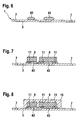
- a printed circuit board carrier 17 This is in FIG. 3 shown.
- the conductive foil 1 with the electronic components 9, 13 has been laminated onto the printed circuit board carrier 17 without the electronic components 9, 13 being enclosed by the polymer mass 15.
- FIG. 5 illustrated embodiment in which the electronic components 9, 13 are enclosed by the polymer mass 15, laminated to the printed circuit board carrier 17. The lamination takes place after known to those skilled in the process.
- the printed circuit board carrier 17 is laminated onto the conductive film 1 in such a way that the electronic components 9, 13 or the electronic components 9, 13 surrounded by the polymer compound 15 are enclosed by the printed circuit board carrier 17.
- the printed circuit board carrier 17 is laminated on the side of the conductive film 1, on which the electronic components 9 are mounted.
- a glass-fiber-reinforced and at the points of the components 9, 13 predrilled, hardened printed circuit board material is placed on the film.
- a prepreg and optionally another cured printed circuit board material is applied.
- This stack is then pressed in a lamination process.
- the cured circuit board material is usually a glass fiber reinforced epoxy resin.
- an epoxy resin is also generally used. However, this is not completely cured. By applying pressure and an elevated temperature, the prepreg completely cures, thereby bonding it to the cured circuit board material.
- the composite of prepreg and cured printed circuit board material forms the printed circuit board carrier 17.
- holes are formed at the connection points of the further electronic components 13 which have no contact points 11 19 in the conductive film 1, comprising the conductive layer 3 and the insulating layer 5, introduced.
- the correct positioning of the holes 19 can be determined by the initially introduced adjustment marks 7. This makes it possible, precisely at the positions where the electrical connections of the other electronic components 13 are located to produce the holes 19.
- the electronic components 9, which have contact points 11, are contacted with their contact points 11 on the conductive layer 3 of the conductive film 1.
- cooling channels 21 are shown in the printed circuit board carrier 17 drilled.
- a laser drilling method is used.
- the holes 19 are produced by a laser drilling method, a second laser is preferably used for the cooling channels 21. But it can also be drilled holes 19 and cooling channels 21 with the same laser.
- the further electronic components 13 are electrically contacted with the conductive layer 3.
- metal 23 is deposited in the holes 19 by methods known to those skilled in the art, for example by electroless metal deposition. This metal connects the terminals of the other electronic components 13 to the conductive layer 3. An electronic contact has been made.
- the metal 23 used for metallization is copper.
- a starting metallization of palladium is generally first deposited without current. This is followed by a galvanic copper deposition.
- the metal 23 may take the form of a sleeve or completely fill the holes 19.
- an electronic assembly 27 is shown.
- the electronic assembly 27 comprises two printed circuit boards 29.
- a dielectric 31 is applied to the printed conductor structure 25 in order to apply a further printed conductor structure 33.
- a dielectric 31 are, for example, epoxy resins or FR4 materials, which are known from printed circuit board technology.
- the application of the dielectric 31 takes place with the usual methods known to the person skilled in the art. For example, it is possible to apply the dielectric 31 by knife coating, painting, printing, laminating, curtain coating, film coating, spray coating or similar methods.
- the dielectric 31 and subsequently a conductive foil are preferably laminated on first. After laminating the dielectric 31 and the conductive foil, holes are first introduced which are then metallized to electrically connect the conductive foil to underlying layers. Subsequently, the further printed conductor structure 33 is worked out of the conductive foil.
- the printed conductor structure 25 of a printed circuit board 29 can be connected to the printed conductor structure 33 of the second printed circuit board 29.
- the electrical contact takes place, for example, by metallizing the wall of the bore 39.
- the conductor track structure 25, 33 can be electrically contacted to the metal core by means of a bore 41 which terminates on the cooling body 37 in the form of a metal core.
- a ground contact can be realized.
- the electrical contact is preferably carried out by means of a metallization.
- the metallization of the bores 39, 41 is produced, for example, by electroless or galvanic metal deposition. Alternatively, it is also possible, for example, to guide a wire through the holes 39, 41.
- FIGS. 6 to 10 a comparative example for producing an electronic module 27 is shown. That in the FIGS. 6 to 10 The method differs from that in the FIGS. 1 to 5 that the conductive film 1 has only one conductive layer 3 and no insulating layer 5. In the conductive film 1, the adjustment marks 7 are introduced. For the attachment of electronic components 9 adhesive 1 43 is applied to the conductive film. The application of the adhesive 43 may be flat or preferably in the form of adhesive dots, as shown in FIG FIG. 6 is shown done.
Description
Die Erfindung betrifft ein Verfahren zur Herstellung einer elektronischen Baugruppe gemäß dem Oberbegriff von Anspruch 1, sowie eine elektronische Baugruppe gemäß dem Oberbegriff des Anspruchs 7.The invention relates to a method for producing an electronic assembly according to the preamble of
Um elektronische Bauelemente, die in elektronischen Baugruppen auf Leiterplatten eingesetzt werden, verkapseln zu können und um die Flächennutzung auf dem elektronischen Schaltungsträger zu steigern, ist es bekannt, die elektronischen Bauelemente in der Leiterplatte aufzunehmen. Hierdurch ist ein Schutz der elektronischen Bauelemente möglich. Aus
Nachteil dieser Baugruppe ist es, dass zunächst Aufnahmen in das Leiterplattensubstrat eingefräst werden, in welches die elektronischen Bauelemente eingesetzt werden. Eine exakte Positionierung der elektronischen Bauelemente ist auf diese Weise nur schwer möglich.Disadvantage of this assembly is that first recordings are milled into the printed circuit board substrate, in which the electronic components are used. An exact positioning of the electronic components is difficult in this way possible.
Aus
Nachteil dieses Verfahrens ist es, dass die Trägerfolie rückstandsfrei entfernt werden muss, um eine funktionsfähige Anbindung der elektrischen Schaltung zu erzielen.Disadvantage of this method is that the carrier film must be removed without residue in order to achieve a functional connection of the electrical circuit.
Ein weiterer Nachteil der aus dem Stand der Technik bekannten Verfahren ist, dass aufgrund der Leiterplattenstruktur die Bestückfläche auf der Leiterplatte begrenzt ist. Zudem sind die Anschlüsse teilweise relativ lang, was bei Anwendungen im Bereich hoher Taktfrequenzen nachteilig ist.Another disadvantage of the known from the prior art method is that due to the circuit board structure, the Bestückfläche is limited to the circuit board. In addition, the connections are sometimes relatively long, which is disadvantageous in applications in the range of high clock frequencies.
Als weiterer Stand der Technik ist in
Ferner ist aus der
Die Aufgabe der Erfindung ist es, die Nachteile des Stands der Technik zu beheben und dadurch ein vereinfachtes Verfahren zur Herstellung einer elektronischen Baugruppe sowie eine elektronische Baugruppe selbst bereitzustellen. Diese Aufgabe wird durch ein Verfahren mit den Merkmalen des Anspruchs 1 sowie eine elektronische Baugruppe mit den Merkmalen des Anspruchs 7 gelöst.The object of the invention is to overcome the disadvantages of the prior art and thereby provide a simplified method for producing an electronic assembly and an electronic assembly itself. This object is achieved by a method having the features of
Das erfindungsgemäße Verfahren zur Herstellung einer elektronischen Baugruppe weist die Merkmale des neuen Anspruchs 1 auf.The inventive method for producing an electronic module has the features of the
Im Sinne der vorliegenden Erfindung sind die Kontaktierungspunkte kleine Erhebungen aus einem leitfähigen Material, die an den Kontaktierungsstellen des elektronischen Bauteils angebracht sind. Die Höhe der Erhebungen entspricht dabei dem Abstand, den das elektronische Bauteil von der elektrisch leitfähigen Folie einnehmen soll. Geeignete Kontaktierungspunkte sind zum Beispiel Lötbumps oder Studbumps. Die Kontaktierungspunkte dienen gleichzeitig zur Ankontaktierung des elektronischen Bauelements an die elektrisch leitfähige Folie. Auf diese Weise werden kurze Anschlüsse realisiert, die insbesondere bei Anwendungen im Bereich hoher Taktfrequenzen vorteilhaft sind. Ein Vorteil ist es, dass hierdurch das elektronische Bauteil schon während der Montage ankontaktiert wird, wodurch sich die Anzahl der Prozessschritte reduzieren lässt. Ein Vorteil der Ankontaktierung der elektronischen Bauteile mit den Kontaktierungspunkten ist, dass kein Platz benötigt wird, oben liegende Anschlüsse des elektronischen Bauelements mit der elektrisch leitfähigen Folie zu verbinden. Auf diese Weise kann eine dichtere Bestückung erfolgen, woraus eine gesteigerte Flächennutzung resultiert.For the purposes of the present invention, the contacting points are small elevations of a conductive material, which are attached to the contacting points of the electronic component. The height of the elevations corresponds to the distance which the electronic component is to occupy from the electrically conductive foil. Suitable contact points are, for example, solder bumps or studbumps. The contacting points simultaneously serve for Ankontaktierung of the electronic component to the electrically conductive film. In this way, short connections are realized, which are particularly advantageous in applications in the range of high clock frequencies. It is an advantage that, as a result, the electronic component is already contacted during assembly, as a result of which the number of process steps can be reduced. An advantage of contacting the electronic components with the contact points is that no space is required to connect the top terminals of the electronic component with the electrically conductive film. In this way, a denser assembly can take place, resulting in an increased land use results.
Ein weiterer Vorteil ist es, dass risikoreiche Mischtechniken, beispielsweise Löten, Kleben und Drahtbonden, in der Fertigung vermieden werden.Another advantage is that risky mixing techniques, such as soldering, gluing and wire bonding, are avoided in manufacturing.
Ein weiterer Vorteil des erfindungsgemäßen Verfahrens ist es, dass sich die elektronischen Bauelemente durch das Befestigen auf der leitfähigen Folie exakt positionieren lassen. Beim anschließenden Auflaminieren der leitfähigen Folie mit dem mindestens einen daran befestigten elektronischen Bauelement auf einen Leiterplattenträger, wobei das mindestens eine elektronische Bauelement in Richtung des Leiterplattenträgers weist, wird das mindestens eine elektronische Bauelement vom Leitungsträger umschlossen. Hierdurch wird das Bauelement vollständig gekapselt. Durch die komplette Kapselung empfindlicher Bauelemente wird eine hohe Zuverlässigkeit der elektronischen Baugruppe erzielt.Another advantage of the method according to the invention is that the electronic components can be positioned precisely by mounting on the conductive foil. During the subsequent lamination of the conductive foil with the at least one electronic component attached thereto to a printed circuit board carrier, wherein the at least one electronic component points in the direction of the printed circuit board carrier, the at least one electronic component is enclosed by the conductor carrier. As a result, the device is completely encapsulated. Due to the complete encapsulation of sensitive components, a high reliability of the electronic module is achieved.
Weiterhin wird eine planare Ausgangsstruktur erzielt, wodurch reproduzierbare Hochfrequenz-Übergänge erzeugt werden.Furthermore, a planar output structure is achieved, whereby reproducible high-frequency transitions are generated.
Durch das Strukturieren der leitfähigen Folie nach dem Auflaminieren auf den Leiterplattenträger werden auf einfache Weise die notwendigen Leiterbahnen hergestellt. Eine schnelle und kostengünstige Fertigung der elektronischen Baugruppe ist hierdurch möglich.By structuring the conductive film after lamination to the circuit board carrier the necessary interconnects are produced in a simple manner. A fast and cost-effective production of the electronic module is thereby possible.
Die leitfähige Folie kann eine isolierende Schicht aufweisen. Das mindestens eine Bauelement wird auf der isolierenden Schicht befestigt, wobei die Kontaktierungspunkte die isolierende Schicht durchbrechen und das Bauelement mit der leitfähigen Folie kontaktieren. Die isolierende Schicht wirkt als Dielektrikum und dient dazu, dass nicht die gesamte aktive Seite des elektronischen Bauelements auf der leitfähigen Folie aufliegt.The conductive foil may comprise an insulating layer. The at least one component is fastened on the insulating layer, wherein the contacting points break through the insulating layer and contact the component with the conductive foil. The insulating layer acts as a dielectric and serves to ensure that not the entire active side of the electronic component rests on the conductive foil.
Zum Befestigen des mindestens einen elektronischen Bauelements wird Klebstoff auf die leitfähige Folie aufgetragen. Der Klebstoff wirkt als Dielektrikum zwischen der leitfähigen Folie und dem mindestens einen elektronischen Bauelement. Auch hier kontaktieren die Kontaktierungspunkte das Bauelement mit der leitfähigen Folie. Vorteil dabei ist, dass eine Beschichtung der leitfähigen Folie nicht notwendig ist. Dies hat gegenüber der beschichteten Folie Kostenvorteile, da das Aufbringen von Klebstoff auf eine Folie kostengünstiger ist als das Beschichten einer Folie.To attach the at least one electronic component, adhesive is applied to the conductive foil. The adhesive acts as a dielectric between the conductive foil and the at least one electronic component. Again, the contacting points contact the device with the conductive foil. The advantage here is that a coating of the conductive film is not necessary. This has cost advantages over the coated film, since the application of adhesive to a film is less expensive than the coating of a film.
Zusätzlich zu den Bauelementen mit Kontaktierungspunkten ist es weiterhin möglich, dass auch mindestens ein weiteres elektronisches Bauelement ohne Kontaktierungspunkte auf einer isolierenden Schicht oder einer Klebstoffschicht auf der leitfähigen Folie befestigt wird.In addition to the components with contact points, it is also possible for at least one further electronic component without contact points to be fixed on an insulating layer or an adhesive layer on the conductive foil.
Vorzugsweise wird das mindestens eine elektronische Bauelement und gegebenenfalls das mindestens eine weitere elektronische Bauelement nach dem Befestigen auf der leitfähigen Folie von einer Polymermasse umschlossen. Das Umschließen des mindestens einen elektronischen Bauelements mit der Polymermasse führt zu einem zusätzlichen Schutz des Bauelements. Hierdurch wird auch bei empfindlichen Bauelementen die Gefahr einer Beschädigung deutlich gemindert.Preferably, the at least one electronic component and, if appropriate, the at least one further electronic component are enclosed by a polymer mass after being attached to the conductive foil. The enclosing of the at least one electronic component with the polymer compound leads to an additional protection of the component. As a result, the risk of damage is significantly reduced even with sensitive components.
Die Polymermasse, mit der das mindestens eine elektronische Bauelement und gegebenenfalls das mindestens eine weitere elektronische Bauelement umschlossen wird, ist zum Beispiel eine Niederdruckpressmasse, beispielsweise eine Epoxy-Niederdruckpressmasse. Die Niederdruckpressmasse wird zum Beispiel durch ein Spritzpressverfahren aufgebracht. In der Polymermasse können zusätzlich Platzhalter, zum Beispiel für dickere Dielektrika, freigehalten werden. Diese können jedoch auch als Einlegeteile beim Umspritzen des mindestens einen elektronischen Bauelements mit umspritzt werden.The polymer composition with which the at least one electronic component and optionally the at least one further electronic component is enclosed is, for example, a low-pressure molding compound, for example an epoxy low-pressure molding compound. The low-pressure molding compound is applied, for example, by a transfer molding process. In addition, wildcards, for example for thicker dielectrics, can be kept free in the polymer compound. However, these can also be encapsulated as inserts during encapsulation of the at least one electronic component.
Das Befestigen des mindestens einen elektronischen Bauelements und gegebenenfalls des mindestens einen weiteren elektronischen Bauelements erfolgt vorzugsweise durch Aufkleben. Hierzu ist es bevorzugt, dass die leitfähige Trägerfolie eine Klebeschicht aufweist. Die Klebeschicht bildet dabei vorzugsweise gleichzeitig die isolierende Schicht. Die leitfähige Folie ist dabei zum Beispiel eine selbstklebende leitfähige Folie. Das Aufkleben kann durch Heiß- und Druckprozesse erfolgen. Dies ist zum Beispiel auch ein Heißklebeprozess. Das Aufkleben des mindestens einen Bauelements und gegebenenfalls des mindestens einen weiteren Bauelements kann durch Auftragen von Klebstoff auf die elektrisch leitfähige Folie erfolgen. Das Auftragen des Klebstoffes kann dabei durch jedes beliebige, dem Fachmann bekannte Verfahren erfolgen. So ist es zum Beispiel möglich, den Klebstoff in Form von Klebstoffpunkten auf die elektrisch leitfähige Folie aufzutragen. Weiterhin ist es auch möglich, die elektrisch leitfähige Folie zum Beispiel mit einer Klebstoffschicht zu bestreichen. Vorzugsweise wird der Klebstoff jedoch in Form von Klebstoffpunkten an den Positionen, an denen elektronische Bauelemente angebracht werden, aufgetragen.The fastening of the at least one electronic component and optionally of the at least one further electronic component is preferably carried out by gluing. For this purpose, it is preferred that the conductive carrier film has an adhesive layer. The adhesive layer preferably forms the insulating layer at the same time. The conductive foil is, for example, a self-adhesive conductive foil. The sticking can be done by hot and pressure processes. This is also a hot glue process, for example. The bonding of the at least one component and optionally of the at least one further component can be done by applying adhesive to the electrically conductive film. The application of the adhesive can be carried out by any known to those skilled in the process. So it is possible, for example, the glue in Apply form of glue dots on the electrically conductive foil. Furthermore, it is also possible to coat the electrically conductive film, for example, with an adhesive layer. Preferably, however, the adhesive is applied in the form of glue dots at the locations where electronic components are mounted.
Die leitfähige Folie, die eingesetzt wird, ist zum Beispiel eine Kupferfolie, wie sie auch als RCC-Material aus der Leiterplattentechnik bekannt ist. Weitere geeignete leitfähige Folien sind beispielsweise LCP-Folien oder PI-Folien. Als Metall eignet sich neben Kupfer zum Beispiel auch Aluminium.The conductive foil used is, for example, a copper foil, also known as printed circuit board RCC material. Other suitable conductive films are, for example, LCP films or PI films. As a metal is suitable in addition to copper, for example, aluminum.
Vor dem Aufbringen des mindestens einen elektronischen Bauelements auf die leitfähige Folie können Justagemarken in die leitfähige Folie eingebracht werden. Die Justagemarken sind zum Beispiel Löcher oder Sacklöcher mit einem beliebigen Querschnitt. Diese können zum Beispiel durch Ätzen, Stanzen oder Bohren in die leitfähige Folie eingebracht werden. Die Justagemarken werden dabei auf der dem mindestens einen elektronischen Bauelement gegenüberliegenden Seite der leitfähigen Folie angebracht. Durch die Justagemarken lässt sich auch nach dem Umschließen des mindestens einen elektronischen Bauelements mit der Polymermasse bzw. nach dem Auflaminieren der leitfähigen Folie auf den Leiterplattenträger die genaue Position des mindestens einen elektronischen Bauelements und gegebenenfalls des mindestens einen weiteren elektronischen Bauelements bestimmen. Dies ist zum einen für die Ausbildung der Leiterbahnstruktur erforderlich, zum anderen ist es für die Kontaktierung des mindestens einen weiteren Bauelements, sofern ein solches ohne Kontaktierungspunkte aufgebracht wird, notwendig. Alternativ eignen sich als Justagemarken zum Beispiel auch Bauelemente, mit denen die leitfähige Folie bestückt ist. An den Stellen, an denen die Bauelemente angeordnet sind, wird die leitfähige Folie vorzugsweise freigebohrt oder geröntgt, um die Bauelemente zu erkennen. Daneben können die Justagemarken selbstverständlich auch jede andere, dem Fachmann bekannte Form aufweisen.Before applying the at least one electronic component to the conductive foil, alignment marks can be introduced into the conductive foil. The Justagemarken are, for example, holes or blind holes with any cross section. These can be introduced, for example, by etching, stamping or drilling in the conductive film. The Justagemarken be mounted on the at least one electronic component opposite side of the conductive film. The alignment marks also allow the exact position of the at least one electronic component and optionally of the at least one further electronic component to be determined after enclosing the at least one electronic component with the polymer mass or after laminating the conductive foil to the printed circuit board carrier. On the one hand, this is necessary for the formation of the conductor track structure; on the other hand, it is necessary for contacting the at least one further component, if such is applied without contacting points. Alternatively suitable as Justagemarken for example, components with which the conductive film is equipped. At the locations where the devices are located, the conductive foil is preferably drilled or x-rayed to detect the devices. In addition, the Justagemarken can of course also any other, known in the art form.
Wenn weitere elektronische Bauelemente, die keine Kontaktierungspunkte aufweisen, aufgesetzt werden, werden an den Positionen, an denen das mindestens eine weitere elektronische Bauelement mit der leitfähigen Trägerfolie elektrisch kontaktiert werden soll, vorzugsweise Löcher eingebracht. Zur Kontaktierung der leitfähigen Folie mit dem mindestens einen weiteren elektronischen Bauelement werden die Löcher zum Beispiel metallisiert. Das Einbringen der Löcher erfolgt zum Bespiel durch Laserbohren. Die Positionen, an denen die Löcher eingebracht werden, werden anhand der Justagemarken bestimmt.If further electronic components which have no contact points are placed, preferably holes are introduced at the positions at which the at least one further electronic component is to be electrically contacted with the conductive carrier foil. For contacting the conductive foil with the at least one further electronic component, the holes are metallized, for example. The introduction of the holes is done for example by laser drilling. The positions at which the holes are inserted are determined by the adjustment marks.
Das Metallisieren der Löcher, um einen Kontakt des mindestens einen weiteren elektronischen Bauelements mit der leitfähigen Trägerfolie zu erzielen, erfolgt nach dem Fachmann bekannten Verfahren. Das Metallisieren kann zum Beispiel durch stromlose Metallabscheidung erfolgen. Die stromlose Metallabscheidung ist ein übliches Verfahren, welches in der Leiterplattenherstellung eingesetzt wird. Das Metallisieren der Löcher erfolgt vorzugsweise mit Kupfer.The metallization of the holes in order to achieve contact of the at least one further electronic component with the conductive carrier foil is carried out by methods known to the person skilled in the art. The metallization may be, for example, by electroless metal deposition respectively. Electroless metal deposition is a common process used in printed circuit board manufacturing. The metallization of the holes is preferably carried out with copper.
Weitere Leiterbahnen lassen sich zum Beispiel dadurch aufbringen, indem auf die in Schritt (c) strukturierte leitfähige Folie weitere Lagen, die Leiterbahnstrukturen enthalten, aufgebracht werden. Hierzu wird vorzugsweise zunächst ein Dielektrikum aufgebracht, durch welches die in Schritt (c) ausgebildeten Leiterbahnen abgedeckt werden. Gleichzeitig erfolgt hierdurch eine Isolierung der Leiterbahnen, damit kein unerwünschter elektrischer Kontakt mit den Leiterbahnen der nachfolgend aufgebrachten Schicht erfolgt. Daran anschließend werden auf das Dielektrikum nach dem Fachmann bekannten Verfahren weitere Leiterbahnen aufgebracht. Die weiteren Lagen, die Leiterbahnen enthalten, können alternativ auch durch Aufbringen weiterer leitfähiger Folien auf die erste Lage und anschließendem Strukturieren der Folie zur Ausbildung von Leiterbahnen hergestellt werden. Die Folien umfassen vorzugsweise eine klebende isolierende Schicht, mit der diese auf die Leiterbahnen aufgebracht werden.Further interconnects can be applied, for example, by applying further layers containing interconnect structures to the conductive film structured in step (c). For this purpose, a dielectric is preferably first applied, by means of which the conductor tracks formed in step (c) are covered. At the same time this results in an isolation of the conductor tracks, so that no unwanted electrical contact with the conductor tracks of the subsequently applied layer takes place. Subsequently, further printed conductors are applied to the dielectric by methods known to the person skilled in the art. The further layers which contain conductor tracks can alternatively also be produced by applying further conductive foils to the first layer and subsequently structuring the foil to form conductor tracks. The films preferably comprise an adhesive insulating layer with which they are applied to the conductor tracks.
Die Kontaktierung zwischen zwei Lagen mit Leiterbahnen erfolgt durch Einbringen von Löchern und anschließendes Metallisieren der Löcher. Alternativ ist es auch möglich, an den Positionen, an denen die Leiterbahnen der zweiten Schicht die Leiterbahnen der ersten Schicht kontaktieren sollen, kein Dielektrikum aufzubringen.The contacting between two layers of printed conductors takes place by introducing holes and then metallizing the holes. Alternatively, it is also possible to apply no dielectric at the positions at which the interconnects of the second layer are to contact the interconnects of the first layer.
Um beim Betrieb der elektronischen Baugruppe entstehende Wärme abzuführen, ist es bevorzugt, dass das mindestens eine elektronische Bauelement nach dem Auflaminieren der leitfähigen Folie auf den Leiterplattenträger in Schritt (b) auf der von der leitfähigen Folie wegweisenden Seite mit einem Kühlkörper kontaktiert wird, so dass der Kühlkörper nach dem Auflaminieren auf den Leiterplattenträger ebenfalls in der Leiterplatte integriert ist. Der Kühlkörper kann dabei jeder beliebige, dem Fachmann bekannte Kühlkörper sein. So ist es zum Beispiel möglich, dass der Kühlkörper ein Metallkern ist. Im Betrieb gibt dann das elektronische Bauelement an den Metallkern Wärme ab, über den diese nach außen abgegeben werden kann.In order to dissipate heat generated during operation of the electronic assembly, it is preferred that the at least one electronic component after contacting the conductive film on the printed circuit board carrier in step (b) is contacted on the facing away from the conductive film side with a heat sink, so that the heat sink is also integrated in the printed circuit board after the lamination to the printed circuit board carrier. The heat sink can be any heat sink known to those skilled in the art. For example, it is possible for the heat sink to be a metal core. During operation, the electronic component then gives off heat to the metal core, via which it can be released to the outside.
Durch das erfindungsgemäße Verfahren lässt sich eine kostengünstige Verdrahtung und Verkapselung erzielen, durch den Einsatz von Prozessen auf vielen Modulen gleichzeitig. Ein weiterer Vorteil ist, dass die elektronische Baugruppe als Standard-Bauteil weiterverarbeitet werden kann.By the method according to the invention, a cost-effective wiring and encapsulation can be achieved by the use of processes on many modules simultaneously. Another advantage is that the electronic module can be further processed as a standard component.
Weiterhin betrifft die Erfindung eine elektronische Baugruppe mit den Merkmalen von Anspruch 7, umfassend mindestens ein elektronisches Bauelement, das mit einer Leiterbahnstruktur auf einer Leiterplatte verbunden ist. Das mindestens eine elektronische Bauelement ist in einem Leiterplattenträger eingebettet und die Leiterbahnstruktur ist an der Oberfläche der Leiterplatte angeordnet. Die Kontaktierung des Bauelements mit der Leiterbahnstruktur erfolgt durch am Bauelement angebrachte Kontaktierungspunkte. Neben der vorstehend schon erwähnten kostengünstigen Verkapselung und damit hohen Zuverlässigkeit wird die teure Substrat- und Packagetechnik, wie sie derzeit im Stand der Technik eingesetzt wird, ersetzt bzw. auf ein kleines Bauelement reduziert. Zudem ist es bei der erfindungsgemäßen elektronischen Baugruppe möglich, eine komplette Hochfrequenz-Schaltung auf einem Modul inklusive Antennen zu konzentrieren. Die erfindungsgemäß hergestellte elektronische Baugruppe kann als Standard-Bauteil weiterverarbeitet werden.Furthermore, the invention relates to an electronic subassembly having the features of
Die Kontaktierungspunkte sind vorzugsweise Lötbumps oder Studbumps. Weiterhin geeignet sind auch galvanisch hergestellte Bumps aus unterschiedlichen Materialien, z.B. Kupfer oder Gold. Durch ein automatisiertes Aufbringen der Lötbumps oder Studbumps ist es möglich, dass diese jeweils eine gleichmäßige Höhe aufweisen. Hierdurch lässt sich ein gleichmäßiger Abstand des elektronischen Bauelements von der leitfähigen Folie erzielen.The contact points are preferably solder bumps or studbumps. Also suitable are electroplated bumps made of different materials, e.g. Copper or gold. By automated application of the Lötbumps or Studbumps it is possible that they each have a uniform height. This makes it possible to achieve a uniform spacing of the electronic component from the conductive foil.
In einer bevorzugten Ausführungsform ist die Leiterbahnstruktur in mehreren Lagen ausgebildet. Hierdurch ist eine gesteigerte Flächennutzung auf einem elektronischen Schaltungsträger möglich. Durch die zusätzlichen Lagen lässt sich die elektronische Baugruppe auf engstem Raum mit Bauteilen bestücken und kontaktieren.In a preferred embodiment, the conductor track structure is formed in a plurality of layers. As a result, an increased land use on an electronic circuit board is possible. Due to the additional layers, the electronic module can be equipped and contacted with components in the smallest possible space.
Um gut Wärme abführen zu können, die beim Betrieb der elektronischen Baugruppe entsteht, ist es bevorzugt, dass in der Leiterplatte ein Kühlkörper enthalten ist. Als Kühlkörper eignet sich zum Beispiel ein Metallkern, an den das mindestens eine elektronische Bauelement metallisch angebunden ist.In order to dissipate good heat that arises during operation of the electronic module, it is preferred that a heat sink is included in the circuit board. As a heat sink, for example, a metal core is suitable, to which the at least one electronic component is connected metallically.
Neben dem mindestens einen elektronischen Bauelement ist es auch möglich, dass die elektronische Baugruppe ein oder mehrere mechanische Bauelemente enthält.In addition to the at least one electronic component, it is also possible for the electronic assembly to contain one or more mechanical components.
Elektronische Bauelemente, die bei dem erfindungsgemäßen Verfahren bzw. bei der erfindungsgemäß ausgebildeten elektronischen Baugruppe eingesetzt werden, sind alle dem Fachmann bekannten elektronischen Bauelemente, wie sie in der Leiterplattentechnologie und Mikroelektronik verwendet werden. Auch als mechanische Bauelemente kommen alle Bauelemente in Betracht, wie sie in der Leiterplattentechnologie eingesetzt werden.Electronic components that are used in the method according to the invention or in the electronic assembly designed according to the invention are all electronic components known to the person skilled in the art, such as are used in printed circuit board technology and microelectronics. As mechanical components, all components come into consideration, as they are used in printed circuit board technology.
Ausführungsbeispiele und Vergleichsbeispiele der Erfindung sind in den Zeichnungen dargestellt und in der nachfolgenden Beschreibung näher erläutert.Embodiments and comparative examples of the invention are illustrated in the drawings and explained in more detail in the following description.
Es zeigen
- Figuren 1-5
- mehrere Schritte der Herstellung einer erfindungsgemäßen Vorrichtung in einer Ausführungsform,
- Figuren 6-10
- mehrere Schritte der Herstellung einer erfindungsgemäßen Vorrichtung in einem Vergleichsbeispiel.
- Figures 1-5
- several steps of producing a device according to the invention in one embodiment,
- Figures 6-10
- several steps of producing a device according to the invention in a comparative example.
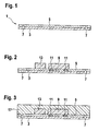
In
Die leitfähige Schicht 3 ist vorzugsweise eine Metallschicht. Besonders bevorzugt als Metall ist Kupfer.The
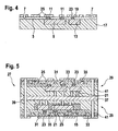
In einem zweiten Schritt werden auf die isolierende Schicht 5 elektronische Bauelemente 9 aufgebracht. Dies ist in
Das Aufbringen der elektronischen Bauelemente 9, der weiteren elektronischen Bauelemente 13 bzw. der mechanischen Bauelemente erfolgt vorzugsweise durch Aufkleben auf die isolierende Schicht 5. Hierbei werden die elektronischen Bauelemente 9, 13 so auf die isolierende Schicht 5 der leitfähigen Folie 1 platziert, wie die elektronischen Bauelemente 9, 13 später in der elektrischen Schaltung angeordnet sein sollen. Es können auf einzelne oder alle elektronischen Bauelemente 9, 13 zum Beispiel Kühlkörper aufgebracht werden, um eine erhöhte Wärmeabfuhr während des Betriebes der elektronischen Bauelemente 9, 13 zu gewährleisten. Die optional vorsehbaren Kühlkörper werden hierbei auf der Seite der elektronischen Bauelemente 9, 13 aufgesetzt, die der leitfähigen Folie 1 abgewandt ist.The application of the
Um eine Kapselung von empfindlichen elektronischen Bauelementen 9, 13 zu erzielen, ist es möglich, diese mit einer Polymermasse 15 zu umschließen. Dies ist zum Beispiel in Figur 5 dargestellt. Die Polymermasse 15 ist zum Beispiel eine Epoxy-Niederdruckpressmasse. In die Polymermasse 15 können, wenn erforderlich, zum Beispiel Platzhalter für dickere Dielektrika, die zum Beispiel für Antennen oder Kühlkörper verwendet werden, umspritzt werden. Das Umhüllen mit der Polymermasse 15 erfolgt zum Beispiel mittels eines Spritzpressverfahrens. Die Platzhalter können zum Beispiel als Vertiefungen oder Wannen ausgeformt sein. Neben dem Spritzpressverfahren ist jedoch auch jedes andere, dem Fachmann bekannte Verfahren, einsetzbar, mit dem sich die elektronischen Bauelemente 9, 13 mit der Polymermasse 15 ummanteln lassen. Zusätzlich hat die Ummantelung mit der Polymermasse 15 den Vorteil, dass ein Höhenausgleich bei Bauelementen 9, 13 mit unterschiedlicher Dicke möglich ist. Dies ist vorteilhaft für den nachfolgenden Laminierprozess. Bauteile können zudem auf abziehbarer Folie vorverkapselt werden und nach dem Abziehen der Folie auf die leitfähige Folie 1 montiert werden.In order to achieve encapsulation of sensitive
Nach dem Aufbringen der elektronischen Bauelemente 9 auf die leitfähige Folie 1 oder, wenn die elektronischen Bauelemente 9, 13 von der Polymermasse umschlossen werden sollen, nach dem Umschließen der elektronischen Bauelemente 9, 13 mit der Polymermasse 15, wird die leitfähige Folie 1 auf Leiterplattenzuschnitt zugeschnitten.After the application of the
Nach dem Zuschneiden wird die leitfähige Folie 1 mit den darauf angebrachten elektronischen Bauelementen 9, 13 und gegebenenfalls weiteren mechanischen Bauelementen, die hier nicht dargestellt sind, auf einen Leiterplattenträger 17 auflaminiert. Dies ist in
Im Allgemeinen wird hierzu bei Bauelementen 9, 13, deren Bauteildicke größer als 0,1 mm ist, zunächst ein glasfaserverstärktes und an den Stellen der Bauelemente 9, 13 vorgebohrtes, ausgehärtetes Leiterplattenmaterial auf die Folie aufgelegt. Hierauf wird ein Prepreg und gegebenenfalls ein weiteres ausgehärtetes Leiterplattenmaterial aufgelegt. Dieser Stapel wird dann in einem Laminierprozess verpresst. Das ausgehärtete Leiterplattenmaterial ist üblicherweise ein glasfaserverstärktes Epoxidharz. Es ist jedoch auch jedes andere geeignete, dem Fachmann bekannte Material einsetzbar. Als Prepreg wird im Allgemeinen ebenfalls ein Epoxidharz eingesetzt. Dieses ist jedoch noch nicht vollständig ausgehärtet. Durch Aufbringen von Druck und einer erhöhten Temperatur härtet das Prepreg vollständig aus, wodurch sich dieses mit dem ausgehärteten Leiterplattenmaterial verbindet. Der Verbund aus Prepreg und ausgehärtetem Leiterplattenmaterial bildet den Leiterplattenträger 17.In general, in the case of
Nach dem Auflaminieren der leitfähigen Folie 1 mit den elektronischen Bauelementen 9, 13 bzw. mit den gegebenenfalls von der Polymermasse 15 umschlossenen elektronischen Bauelementen 9, 13 auf den Leiterplattenträger 17 werden an den Anschlussstellen der weiteren elektronischen Bauelemente 13, die keine Kontaktpunkte 11 aufweisen, Löcher 19 in die leitfähige Folie 1, umfassend die leitfähige Schicht 3 und die isolierende Schicht 5, eingebracht. Die richtige Positionierung der Löcher 19 kann durch die anfangs eingebrachten Justagemarken 7 ermittelt werden. Hierdurch ist es möglich, genau an den Positionen, an denen sich die elektrischen Anschlüsse der weiteren elektronischen Bauelemente 13 befinden, die Löcher 19 zu erzeugen. Die elektronischen Bauelemente 9, die Kontaktpunkte 11 aufweisen, werden mit ihren Kontaktpunkten 11 an der leitfähigen Schicht 3 der leitfähigen Folie 1 kontaktiert.After lamination of the
Üblicherweise werden gleichzeitig mit dem Einbringen der Löcher 19 zur Kontaktierung der weiteren elektronischen Bauelemente 13 mit der leitfähigen Schicht 3 oder direkt im Anschluss daran Kühlkanäle 21, wie sie in der
Durch Metallisierung werden die weiteren elektronischen Bauelemente 13 mit der leitfähigen Schicht 3 elektrisch kontaktiert. Dies ist in
Nach dem Einbringen der Löcher 19 für die Kontaktierung der weiteren elektronischen Bauelemente 13 in die leitfähige Folie 1 und der Metallisierung der Löcher 19 wird die leitfähige Schicht 3, wie in
Durch die Strukturierung der leitfähigen Schicht werden die für die Leiterplatte notwendigen Leiterbahnstrukturen 25 erzeugt.By structuring the conductive layer necessary for the circuit
Durch das Einbetten der elektronischen Bauelemente 9, 13 in den Leiterplattenträger 17 wird eine ebene Oberfläche erzielt. Hierdurch ist eine einfache Verarbeitung der Oberfläche möglich. Selbstverständlich ist es jedoch auch möglich, zuerst die Leiterbahnstruktur 25 aus der leitfähigen Folie 1 auszuarbeiten und daran anschließend die Löcher in die lcitfähige Folie 1 einzubringen und zu metallisieren.By embedding the
In
Auf das Dielektrikum 31 wird eine weitere Leiterbahnstruktur 33 aufgebracht. Hierzu ist es möglich, zunächst vollflächig eine leitfähige Schicht aufzutragen, die anschließend strukturiert wird.On the dielectric 31, a
Bevorzugt ist es auch möglich, auf die erste Leiterbahnstruktur 25 eine weitere leitfähige Folie aufzutragen und aus der leitfähigen Schicht der zweiten leitfähigen Folie die Leiterbahnstruktur 33 zu strukturieren. Dies erfolgt dann vorzugsweise nach dem gleichen Verfahren wie die Strukturierung der leitfähigen Schicht 3 zur Leiterbahnstruktur 25. Nach dem Herstellen der Leiterbahnstruktur 33 können Löcher 35 in das Dielektrikum 31 eingebracht werden, durch die mittels Metallisierung eine Kontaktierung der Leiterbahnstruktur 25 mit der weiteren Leiterbahnstruktur 33 erfolgt.It is also preferably possible to apply a further conductive film to the first printed
Besonders bevorzugt werden zur Herstellung mehrerer leitfähiger, zu Leiterbahnen strukturierter Schichten zunächst das Dielektrikum 31 und anschließend eine leitfähige Folie auflaminiert. Nach dem Auflaminieren des Dielektrikums 31 und der leitfähigen Folie werden zunächst Löcher eingebracht, die anschließend metallisiert werden, um die leitfähige Folie mit darunterliegenden Schichten elektrisch zu verbinden. Daran anschließend wird aus der leitfähigen Folie die weitere Leiterbahnstruktur 33 herausgearbeitet.For the production of a plurality of conductive layers patterned to conductor tracks, the dielectric 31 and subsequently a conductive foil are preferably laminated on first. After laminating the dielectric 31 and the conductive foil, holes are first introduced which are then metallized to electrically connect the conductive foil to underlying layers. Subsequently, the further printed
Um Wärme von den elektronischen Bauelementen 9, 13 abzuführen, ist es möglich, an der den Leiterbahnstrukturen 25, 33 abgewandten Seite der elektronischen Bauelemente 9, 13 Kühlkanäle 21 in den Leiterplattenträger 17 einzubringen. Die Kühlkanäle 21 können mit einem Kühlkörper 37 verbunden werden. In der in
Weiterhin ist es auch möglich, zwischen dem als Metallkern ausgebildeten Kühlkörper 37 und dem elektronischen Bauelement 9, 13 Kühlelemente vorzusehen. Auch ist es möglich, den Metallkern so zu gestalten, dass dieser die elektronischen Bauelemente 9, 13 direkt kontaktiert.Furthermore, it is also possible to provide
Die Verbindung der Leiterplatten 29 erfolgt vorzugsweise ebenfalls mittels eines Laminierprozesses, wie dies bei Leiterplattenherstellungsprozessen üblich ist.The connection of the printed
Mit einer Bohrung 39, die durch beide Leiterplatten 29 hindurchführt, lässt sich die Leiterbahnstruktur 25 der einen Leiterplatte 29 mit der Leiterbahnstruktur 33 der zweiten Leiterplatte 29 verbinden. Der elektrische Kontakt erfolgt zum Beispiel durch eine Metallisierung der Wandung der Bohrung 39. Mittels einer Bohrung 41, die auf dem als Metallkern ausgebildeten Kühlkörper 37 endet, kann die Leiterbahnstruktur 25, 33 mit dem Metallkern elektrisch kontaktiert werden. Hierdurch lässt sich zum Beispiel ein Massekontakt realisieren. Auch bei der Bohrung 41 erfolgt der elektrische Kontakt vorzugsweise mittels einer Metallisierung. Die Metallisierung der Bohrungen 39, 41 wird zum Beispiel durch stromlose oder galvanische Metallabscheidung erzeugt. Alternativ ist es aber zum Beispiel auch möglich, einen Draht durch die Bohrungen 39, 41 zu führen.With a
In den
Auf die Klebepunkte 43 werden die elektronischen Bauelemente 9, die mit Kontaktpunkten 11 versehen sind, aufgesetzt. Durch die Kontaktpunkte 11 wird der Abstand der elektronischen Bauelemente 9 zur leitfähigen Folie 1 festgelegt. Der Klebstoff 43 füllt den Zwischenraum zwischen dem elektronischen Bauelement 9 und der leitfähigen Folie 1 aus und bildet ein Dielektrikum, so dass die elektronischen Bauelemente 9 nicht mit ihrer aktiven Seite direkt auf der leitfähigen Folie 1 aufliegen. Dies ist in
Um eine Kapselung von empfindlichen elektronischen Bauelementen 9 zu erzielen, ist es möglich, diese mit der Polymermasse 15 zu umschließen. Dies ist in
Wie auch bei der in den
Vor dem Strukturieren der leitfähigen Folie 1 zur Leiterbahnstruktur 25 wird auch bei dem in den
In
Claims (9)
- Method for the production of an electronic assembly (27), comprising a circuit board with at least one electronic component (9, 13), which comprises the following steps:(a) fastening at least one electronic component (9) having contacting points (11) on a conductive film (1), the active side of the at least one electronic component facing in the direction of the conductive film (1) and the contacting points (11) being arranged at contacting locations on the active side of the electronic component (9), the contacting points being small elevations of a conductive material that are attached at the contacting locations of the electronic component and the height of the elevations corresponding to the distance from the electrically conductive film that the electronic component is intended to assume, and adhesive (43) being applied to the conductive film (1) to fasten the at least one electronic component (9), the adhesive (43) acting as a dielectric between the conductive film (1) and the at least one electronic component (9) and the contacting points (11) establishing the contact between the component (9) and the conductive film (1), short connections being realized and a planar starting structure for reproducible high-frequency junctions being created,(b) laminating the conductive film (1) with the at least one electronic component (9, 13) fastened thereto onto a circuit board carrier (17), the at least one electronic component (9, 13) facing in the direction of the circuit board carrier (17),(c) after adhesively attaching the at least one electronic component (9) to the conductive film (1) and laminating the conductive film (1) onto the circuit board carrier (17), forming a strip conductor pattern (25) by patterning the conductive film (1),characterized in that
at least one further electronic component (13) without contacting points is fastened on an insulating layer (5) or an adhesive layer (43) on the conductive film (1), and
holes (19) are introduced into the conductive film (1) at the positions at which the electrical contact is intended to be established between the at least one further electronic component (13) and the conductive film (1), and the holes (19) for establishing the contact between the conductive film (1) and the at least one further electronic component (13) are metallized. - Method according to Claim 1, characterized in that the conductive film (1) has an insulating layer (5) and the at least one component (9) is fastened on the insulating layer (5), the contacting points (11) breaking through the insulating layer (5) and establishing the contact between the component (9) and the conductive film (1).
- Method according to either of Claims 1 and 2, characterized in that the at least one electronic component (9, 13) is enclosed by a polymer compound (15) after being fastened on the conductive film (1).
- Method according to one of Claims 1 to 3, characterized in that, before the fastening of the at least one electronic component (9, 13) on the conductive film (1) in step (a), adjusting marks (7) are introduced into the conductive film (1).
- Method according to one of Claims 1 to 4, characterized in that further layers that contain strip conductor patterns (33) are applied to the conductive film (1) patterned in step (c).
- Method according to one of Claims 1 to 5, characterized in that, before the lamination in step (b), the at least one electronic component (9, 13) is brought into contact with a heat sink (37) on the side facing away from the conductive film (1), so that, after the lamination onto the circuit board carrier (17), the heat sink (37) is likewise integrated in the circuit board (29).
- Electronic assembly, comprising at least one electronic component (9, 13), which is connected to a strip conductor pattern (25, 33) on a circuit board (29), the at least one electronic component (9, 13) being embedded in a circuit board carrier (17) and the strip conductor pattern (25, 33) being arranged on the surface of the circuit board (29), the contacting of the component (9) with the strip conductor pattern (25) taking place by contacting points (11) attached to the component (9), the contacting points being small elevations of a conductive material that are attached at the contacting locations of the electronic component and the height of the elevations corresponding to the distance from the electrically conductive film that the electronic component assumes, short connections and a planar starting structure for reproducible high-frequency junctions having been formed, and adhesive (43) having been applied to the conductive film (1) to fasten the at least one electronic component (9), the adhesive (43) acting as a dielectric between the conductive film (1) and the at least one electronic component (9) and the contacting points (11) establishing the contact between the component (9) and the conductive film (1),
characterized in that
at least one further electronic component (13) without contacting points has been fastened on an insulating layer (5) or an adhesive layer (43) on the conductive film (1), holes (19) having been introduced into the conductive film (1) at the positions at which the electrical contact was intended to be established between the at least one further electronic component (13) and the conductive film (1), and the holes (19) for establishing the contact between the conductive film (1) and the at least one further electronic component (13) having been metallized, and
the electronic assembly can be produced in a method according to one of Claims 1 to 6. - Electronic assembly according to Claim 7, characterized in that the contacting points (11) are solder bumps or stud bumps.
- Electronic assembly according to Claim 7 or 8, characterized in that the strip conductor pattern (25, 33) is formed in a number of layers.
Applications Claiming Priority (2)
| Application Number | Priority Date | Filing Date | Title |
|---|---|---|---|
| DE200810000842 DE102008000842A1 (en) | 2008-03-27 | 2008-03-27 | Method for producing an electronic assembly |
| PCT/EP2009/052953 WO2009118249A1 (en) | 2008-03-27 | 2009-03-13 | Method for the production of an electronic assembly |
Publications (2)
| Publication Number | Publication Date |
|---|---|
| EP2260683A1 EP2260683A1 (en) | 2010-12-15 |
| EP2260683B1 true EP2260683B1 (en) | 2013-05-15 |
Family
ID=40791154
Family Applications (1)
| Application Number | Title | Priority Date | Filing Date |
|---|---|---|---|
| EP09725562.4A Active EP2260683B1 (en) | 2008-03-27 | 2009-03-13 | Method for the production of an electronic assembly |
Country Status (6)
| Country | Link |
|---|---|
| US (1) | US20110088936A1 (en) |
| EP (1) | EP2260683B1 (en) |
| JP (1) | JP2011515862A (en) |
| CN (1) | CN101982025B (en) |
| DE (1) | DE102008000842A1 (en) |
| WO (1) | WO2009118249A1 (en) |
Families Citing this family (16)
| Publication number | Priority date | Publication date | Assignee | Title |
|---|---|---|---|---|
| DE102007024189A1 (en) * | 2007-05-24 | 2008-11-27 | Robert Bosch Gmbh | Method for producing an electronic assembly |
| JPWO2009147936A1 (en) * | 2008-06-02 | 2011-10-27 | イビデン株式会社 | Manufacturing method of multilayer printed wiring board |
| US8966747B2 (en) | 2011-05-11 | 2015-03-03 | Vlt, Inc. | Method of forming an electrical contact |
| DE102012213916A1 (en) * | 2011-11-08 | 2013-05-08 | Robert Bosch Gmbh | Electronic module for a control unit |
| DE102011088256A1 (en) * | 2011-12-12 | 2013-06-13 | Zf Friedrichshafen Ag | Multilayer printed circuit board and arrangement with such |
| US9536798B2 (en) * | 2012-02-22 | 2017-01-03 | Cyntec Co., Ltd. | Package structure and the method to fabricate thereof |
| JP5406389B2 (en) | 2012-03-01 | 2014-02-05 | 株式会社フジクラ | Component built-in substrate and manufacturing method thereof |
| FI125959B (en) | 2013-05-10 | 2016-04-29 | Murata Manufacturing Co | A microelectromechanical device and a method for manufacturing a microelectromechanical device |
| DE102013217146A1 (en) * | 2013-08-28 | 2015-03-05 | Carl Zeiss Smt Gmbh | Optical component |
| EP2911486A1 (en) * | 2014-02-19 | 2015-08-26 | AT & S Austria Technologie & Systemtechnik Aktiengesellschaft | PCB-based connector device |
| US20150351218A1 (en) * | 2014-05-27 | 2015-12-03 | Fujikura Ltd. | Component built-in board and method of manufacturing the same, and mounting body |
| KR102333559B1 (en) | 2015-05-11 | 2021-12-01 | 삼성전자 주식회사 | Antenna device and electronic device including the same |
| EP3562281A1 (en) | 2018-04-25 | 2019-10-30 | Siemens Aktiengesellschaft | Baking tray and method for its manufacture |
| FR3090264B1 (en) * | 2018-12-13 | 2022-01-07 | St Microelectronics Grenoble 2 | Component mounting process |
| EP3709777A1 (en) | 2019-03-11 | 2020-09-16 | AT & S Austria Technologie & Systemtechnik Aktiengesellschaft | Solder-free component carrier connection using an elastic element, and method |
| DE102019123193A1 (en) * | 2019-08-29 | 2021-03-04 | Endress+Hauser SE+Co. KG | Field device of automation technology |
Family Cites Families (20)
| Publication number | Priority date | Publication date | Assignee | Title |
|---|---|---|---|---|
| JP3598060B2 (en) * | 1999-12-20 | 2004-12-08 | 松下電器産業株式会社 | CIRCUIT COMPONENT MODULE, MANUFACTURING METHOD THEREOF, AND RADIO DEVICE |
| US6538210B2 (en) * | 1999-12-20 | 2003-03-25 | Matsushita Electric Industrial Co., Ltd. | Circuit component built-in module, radio device having the same, and method for producing the same |
| US6512182B2 (en) | 2001-03-12 | 2003-01-28 | Ngk Spark Plug Co., Ltd. | Wiring circuit board and method for producing same |
| FI119215B (en) * | 2002-01-31 | 2008-08-29 | Imbera Electronics Oy | A method for immersing a component in a substrate and an electronic module |
| US6919508B2 (en) * | 2002-11-08 | 2005-07-19 | Flipchip International, Llc | Build-up structures with multi-angle vias for chip to chip interconnects and optical bussing |
| US7006359B2 (en) * | 2003-07-14 | 2006-02-28 | Avx Corporation | Modular electronic assembly and method of making |
| FI20031201A (en) | 2003-08-26 | 2005-02-27 | Imbera Electronics Oy | Procedure for manufacturing an electronics module and an electronics module |
| DE10353676B4 (en) * | 2003-11-17 | 2007-11-29 | Siemens Ag | Method of making an ultrathin module with rough contacts |
| FI20040592A (en) * | 2004-04-27 | 2005-10-28 | Imbera Electronics Oy | Conducting heat from an inserted component |
| JP2006165175A (en) * | 2004-12-06 | 2006-06-22 | Alps Electric Co Ltd | Circuit component module, electronic circuit device, and circuit component module manufacturing method |
| EP1684341A3 (en) * | 2005-01-21 | 2007-01-10 | Robert Bosch Gmbh | Electric circuit and method of manufacturing an electric circuit |
| DE102005003125A1 (en) | 2005-01-21 | 2006-07-27 | Robert Bosch Gmbh | High-frequency electrical circuit for multi-chip module, has electrical components mechanically connected with each other by sealing compound and provided with conductive strip layers, which electrically connects components with each other |
| KR100716826B1 (en) * | 2005-05-10 | 2007-05-09 | 삼성전기주식회사 | Manufacturing method of printed circuit board with embedded Electronic Component |
| JP2008544512A (en) * | 2005-06-16 | 2008-12-04 | イムベラ エレクトロニクス オサケユキチュア | Circuit board structure and manufacturing method thereof |
| JP2007227586A (en) * | 2006-02-23 | 2007-09-06 | Cmk Corp | Substrate incorporating semiconductor element, and method of manufacturing same |
| KR100770874B1 (en) * | 2006-09-07 | 2007-10-26 | 삼성전자주식회사 | Printed circuit board with embedded integrated circuit |
| US8174119B2 (en) * | 2006-11-10 | 2012-05-08 | Stats Chippac, Ltd. | Semiconductor package with embedded die |
| DE102007015819A1 (en) * | 2007-03-30 | 2008-10-09 | Robert Bosch Gmbh | Method for producing an electronic assembly and electronic assembly |
| DE102007044754A1 (en) * | 2007-09-19 | 2009-04-09 | Robert Bosch Gmbh | Method for producing an electronic assembly and electronic assembly |
| US8375577B2 (en) * | 2008-06-04 | 2013-02-19 | National Semiconductor Corporation | Method of making foil based semiconductor package |
-
2008
- 2008-03-27 DE DE200810000842 patent/DE102008000842A1/en not_active Withdrawn
-
2009
- 2009-03-13 EP EP09725562.4A patent/EP2260683B1/en active Active
- 2009-03-13 JP JP2011501170A patent/JP2011515862A/en active Pending
- 2009-03-13 CN CN200980110836.4A patent/CN101982025B/en active Active
- 2009-03-13 WO PCT/EP2009/052953 patent/WO2009118249A1/en active Application Filing
- 2009-03-13 US US12/736,045 patent/US20110088936A1/en not_active Abandoned
Also Published As
| Publication number | Publication date |
|---|---|
| US20110088936A1 (en) | 2011-04-21 |
| WO2009118249A1 (en) | 2009-10-01 |
| CN101982025B (en) | 2014-09-10 |
| JP2011515862A (en) | 2011-05-19 |
| EP2260683A1 (en) | 2010-12-15 |
| CN101982025A (en) | 2011-02-23 |
| DE102008000842A1 (en) | 2009-10-01 |
Similar Documents
| Publication | Publication Date | Title |
|---|---|---|
| EP2260683B1 (en) | Method for the production of an electronic assembly | |
| EP2286644B1 (en) | Method for integrating at least one electronic component into a printed circuit board, and printed circuit board | |
| DE112004001727B4 (en) | Method of manufacturing an electronic module | |
| EP2259311B1 (en) | Method for embedding at least one component into a circuit board element | |
| DE60300619T2 (en) | METHOD FOR EMBEDDING A COMPONENT INTO A BASIS AND FOR FORMING A CONTACT | |
| EP3231261B1 (en) | Printed circuit board with asymmetrical stack of layers | |
| EP2153707B1 (en) | Method for producing an electronic assembly | |
| DE112005000952T5 (en) | Electronic module and method of making the same | |
| WO2006077208A1 (en) | Control module | |
| EP3231262B1 (en) | Semi-flexible printed circuit board with embedded component | |
| AT13055U1 (en) | METHOD FOR INTEGRATING AN ELECTRONIC COMPONENT INTO A CONDUCTOR PLATE OR A PCB INTERMEDIATE PRODUCT AND PCB OR INTERMEDIATE CIRCUIT PRODUCT | |
| DE102005003125A1 (en) | High-frequency electrical circuit for multi-chip module, has electrical components mechanically connected with each other by sealing compound and provided with conductive strip layers, which electrically connects components with each other | |
| EP3399546A1 (en) | Electronic assembly having a built-in component between two substrates and method for the production of same | |
| EP2193697A2 (en) | Method for the production of an electronic assembly, and electronic assembly | |
| EP2421339A1 (en) | Method for embedding electrical components | |
| WO2011082778A2 (en) | Method for producing an electronic unit and electronic unit | |
| DE3931551C2 (en) | Method of making a substrate | |
| EP2982226B1 (en) | Method for producing a circuit board element | |
| WO2009098033A1 (en) | Method for producing a printed circuit board | |
| WO2008119586A1 (en) | Method for the production of an electronic assembly, and electronic assembly | |
| DE202009009950U1 (en) | Electronic module | |
| EP1684341A2 (en) | Electric circuit and method of manufacturing an electric circuit | |
| DE102018204553B4 (en) | Power electronics module for automotive applications | |
| EP2148364A2 (en) | Contacting method for substrate-based switches and accompanying switch assembly | |
| DE19549647C2 (en) | High-density packaging multi-chip semiconductor module |
Legal Events
| Date | Code | Title | Description |
|---|---|---|---|
| PUAI | Public reference made under article 153(3) epc to a published international application that has entered the european phase |
Free format text: ORIGINAL CODE: 0009012 |
|
| 17P | Request for examination filed |
Effective date: 20101027 |
|
| AK | Designated contracting states |
Kind code of ref document: A1 Designated state(s): AT BE BG CH CY CZ DE DK EE ES FI FR GB GR HR HU IE IS IT LI LT LU LV MC MK MT NL NO PL PT RO SE SI SK TR |
|
| AX | Request for extension of the european patent |
Extension state: AL BA RS |
|
| 17Q | First examination report despatched |
Effective date: 20110419 |
|
| DAX | Request for extension of the european patent (deleted) | ||
| REG | Reference to a national code |
Ref country code: DE Ref legal event code: R079 Ref document number: 502009007103 Country of ref document: DE Free format text: PREVIOUS MAIN CLASS: H05K0001180000 Ipc: H05K0003300000 |
|
| GRAP | Despatch of communication of intention to grant a patent |
Free format text: ORIGINAL CODE: EPIDOSNIGR1 |
|
| RIC1 | Information provided on ipc code assigned before grant |
Ipc: H01L 23/538 20060101ALI20121206BHEP Ipc: H01L 23/367 20060101ALI20121206BHEP Ipc: H01L 25/065 20060101ALI20121206BHEP Ipc: H05K 1/18 20060101ALI20121206BHEP Ipc: H05K 3/30 20060101AFI20121206BHEP |
|
| GRAS | Grant fee paid |
Free format text: ORIGINAL CODE: EPIDOSNIGR3 |
|
| GRAA | (expected) grant |
Free format text: ORIGINAL CODE: 0009210 |
|
| AK | Designated contracting states |
Kind code of ref document: B1 Designated state(s): AT BE BG CH CY CZ DE DK EE ES FI FR GB GR HR HU IE IS IT LI LT LU LV MC MK MT NL NO PL PT RO SE SI SK TR |
|
| REG | Reference to a national code |
Ref country code: GB Ref legal event code: FG4D Free format text: NOT ENGLISH Ref country code: CH Ref legal event code: EP |
|
| REG | Reference to a national code |
Ref country code: AT Ref legal event code: REF Ref document number: 612676 Country of ref document: AT Kind code of ref document: T Effective date: 20130615 |
|
| REG | Reference to a national code |
Ref country code: IE Ref legal event code: FG4D Free format text: LANGUAGE OF EP DOCUMENT: GERMAN |
|
| REG | Reference to a national code |
Ref country code: DE Ref legal event code: R096 Ref document number: 502009007103 Country of ref document: DE Effective date: 20130711 |
|
| REG | Reference to a national code |
Ref country code: LT Ref legal event code: MG4D |
|
| REG | Reference to a national code |
Ref country code: NL Ref legal event code: VDEP Effective date: 20130515 |
|
| PG25 | Lapsed in a contracting state [announced via postgrant information from national office to epo] |
Ref country code: SE Free format text: LAPSE BECAUSE OF FAILURE TO SUBMIT A TRANSLATION OF THE DESCRIPTION OR TO PAY THE FEE WITHIN THE PRESCRIBED TIME-LIMIT Effective date: 20130515 Ref country code: PT Free format text: LAPSE BECAUSE OF FAILURE TO SUBMIT A TRANSLATION OF THE DESCRIPTION OR TO PAY THE FEE WITHIN THE PRESCRIBED TIME-LIMIT Effective date: 20130916 Ref country code: NO Free format text: LAPSE BECAUSE OF FAILURE TO SUBMIT A TRANSLATION OF THE DESCRIPTION OR TO PAY THE FEE WITHIN THE PRESCRIBED TIME-LIMIT Effective date: 20130815 Ref country code: ES Free format text: LAPSE BECAUSE OF FAILURE TO SUBMIT A TRANSLATION OF THE DESCRIPTION OR TO PAY THE FEE WITHIN THE PRESCRIBED TIME-LIMIT Effective date: 20130826 Ref country code: LT Free format text: LAPSE BECAUSE OF FAILURE TO SUBMIT A TRANSLATION OF THE DESCRIPTION OR TO PAY THE FEE WITHIN THE PRESCRIBED TIME-LIMIT Effective date: 20130515 Ref country code: GR Free format text: LAPSE BECAUSE OF FAILURE TO SUBMIT A TRANSLATION OF THE DESCRIPTION OR TO PAY THE FEE WITHIN THE PRESCRIBED TIME-LIMIT Effective date: 20130816 Ref country code: IS Free format text: LAPSE BECAUSE OF FAILURE TO SUBMIT A TRANSLATION OF THE DESCRIPTION OR TO PAY THE FEE WITHIN THE PRESCRIBED TIME-LIMIT Effective date: 20130915 Ref country code: SI Free format text: LAPSE BECAUSE OF FAILURE TO SUBMIT A TRANSLATION OF THE DESCRIPTION OR TO PAY THE FEE WITHIN THE PRESCRIBED TIME-LIMIT Effective date: 20130515 Ref country code: FI Free format text: LAPSE BECAUSE OF FAILURE TO SUBMIT A TRANSLATION OF THE DESCRIPTION OR TO PAY THE FEE WITHIN THE PRESCRIBED TIME-LIMIT Effective date: 20130515 |
|
| PG25 | Lapsed in a contracting state [announced via postgrant information from national office to epo] |
Ref country code: PL Free format text: LAPSE BECAUSE OF FAILURE TO SUBMIT A TRANSLATION OF THE DESCRIPTION OR TO PAY THE FEE WITHIN THE PRESCRIBED TIME-LIMIT Effective date: 20130515 Ref country code: BG Free format text: LAPSE BECAUSE OF FAILURE TO SUBMIT A TRANSLATION OF THE DESCRIPTION OR TO PAY THE FEE WITHIN THE PRESCRIBED TIME-LIMIT Effective date: 20130815 Ref country code: HR Free format text: LAPSE BECAUSE OF FAILURE TO SUBMIT A TRANSLATION OF THE DESCRIPTION OR TO PAY THE FEE WITHIN THE PRESCRIBED TIME-LIMIT Effective date: 20130515 |
|
| PG25 | Lapsed in a contracting state [announced via postgrant information from national office to epo] |
Ref country code: LV Free format text: LAPSE BECAUSE OF FAILURE TO SUBMIT A TRANSLATION OF THE DESCRIPTION OR TO PAY THE FEE WITHIN THE PRESCRIBED TIME-LIMIT Effective date: 20130515 |
|
| PG25 | Lapsed in a contracting state [announced via postgrant information from national office to epo] |
Ref country code: SK Free format text: LAPSE BECAUSE OF FAILURE TO SUBMIT A TRANSLATION OF THE DESCRIPTION OR TO PAY THE FEE WITHIN THE PRESCRIBED TIME-LIMIT Effective date: 20130515 Ref country code: EE Free format text: LAPSE BECAUSE OF FAILURE TO SUBMIT A TRANSLATION OF THE DESCRIPTION OR TO PAY THE FEE WITHIN THE PRESCRIBED TIME-LIMIT Effective date: 20130515 Ref country code: CZ Free format text: LAPSE BECAUSE OF FAILURE TO SUBMIT A TRANSLATION OF THE DESCRIPTION OR TO PAY THE FEE WITHIN THE PRESCRIBED TIME-LIMIT Effective date: 20130515 Ref country code: DK Free format text: LAPSE BECAUSE OF FAILURE TO SUBMIT A TRANSLATION OF THE DESCRIPTION OR TO PAY THE FEE WITHIN THE PRESCRIBED TIME-LIMIT Effective date: 20130515 |
|
| PG25 | Lapsed in a contracting state [announced via postgrant information from national office to epo] |
Ref country code: IT Free format text: LAPSE BECAUSE OF FAILURE TO SUBMIT A TRANSLATION OF THE DESCRIPTION OR TO PAY THE FEE WITHIN THE PRESCRIBED TIME-LIMIT Effective date: 20130515 Ref country code: NL Free format text: LAPSE BECAUSE OF FAILURE TO SUBMIT A TRANSLATION OF THE DESCRIPTION OR TO PAY THE FEE WITHIN THE PRESCRIBED TIME-LIMIT Effective date: 20130515 Ref country code: RO Free format text: LAPSE BECAUSE OF FAILURE TO SUBMIT A TRANSLATION OF THE DESCRIPTION OR TO PAY THE FEE WITHIN THE PRESCRIBED TIME-LIMIT Effective date: 20130515 |
|
| PLBE | No opposition filed within time limit |
Free format text: ORIGINAL CODE: 0009261 |
|
| STAA | Information on the status of an ep patent application or granted ep patent |
Free format text: STATUS: NO OPPOSITION FILED WITHIN TIME LIMIT |
|
| 26N | No opposition filed |
Effective date: 20140218 |
|
| REG | Reference to a national code |
Ref country code: DE Ref legal event code: R097 Ref document number: 502009007103 Country of ref document: DE Effective date: 20140218 |
|
| PG25 | Lapsed in a contracting state [announced via postgrant information from national office to epo] |
Ref country code: LU Free format text: LAPSE BECAUSE OF FAILURE TO SUBMIT A TRANSLATION OF THE DESCRIPTION OR TO PAY THE FEE WITHIN THE PRESCRIBED TIME-LIMIT Effective date: 20140313 |
|
| REG | Reference to a national code |
Ref country code: CH Ref legal event code: PL |
|
| REG | Reference to a national code |
Ref country code: IE Ref legal event code: MM4A |
|
| PG25 | Lapsed in a contracting state [announced via postgrant information from national office to epo] |
Ref country code: CH Free format text: LAPSE BECAUSE OF NON-PAYMENT OF DUE FEES Effective date: 20140331 Ref country code: LI Free format text: LAPSE BECAUSE OF NON-PAYMENT OF DUE FEES Effective date: 20140331 Ref country code: IE Free format text: LAPSE BECAUSE OF NON-PAYMENT OF DUE FEES Effective date: 20140313 |
|
| REG | Reference to a national code |
Ref country code: AT Ref legal event code: MM01 Ref document number: 612676 Country of ref document: AT Kind code of ref document: T Effective date: 20140313 |
|
| PG25 | Lapsed in a contracting state [announced via postgrant information from national office to epo] |
Ref country code: AT Free format text: LAPSE BECAUSE OF NON-PAYMENT OF DUE FEES Effective date: 20140313 |
|
| PG25 | Lapsed in a contracting state [announced via postgrant information from national office to epo] |
Ref country code: MT Free format text: LAPSE BECAUSE OF FAILURE TO SUBMIT A TRANSLATION OF THE DESCRIPTION OR TO PAY THE FEE WITHIN THE PRESCRIBED TIME-LIMIT Effective date: 20130515 |
|
| REG | Reference to a national code |
Ref country code: FR Ref legal event code: PLFP Year of fee payment: 8 |
|
| PG25 | Lapsed in a contracting state [announced via postgrant information from national office to epo] |
Ref country code: MC Free format text: LAPSE BECAUSE OF FAILURE TO SUBMIT A TRANSLATION OF THE DESCRIPTION OR TO PAY THE FEE WITHIN THE PRESCRIBED TIME-LIMIT Effective date: 20130515 |
|
| PG25 | Lapsed in a contracting state [announced via postgrant information from national office to epo] |
Ref country code: CY Free format text: LAPSE BECAUSE OF FAILURE TO SUBMIT A TRANSLATION OF THE DESCRIPTION OR TO PAY THE FEE WITHIN THE PRESCRIBED TIME-LIMIT Effective date: 20130515 |
|
| PG25 | Lapsed in a contracting state [announced via postgrant information from national office to epo] |
Ref country code: HU Free format text: LAPSE BECAUSE OF FAILURE TO SUBMIT A TRANSLATION OF THE DESCRIPTION OR TO PAY THE FEE WITHIN THE PRESCRIBED TIME-LIMIT; INVALID AB INITIO Effective date: 20090313 Ref country code: TR Free format text: LAPSE BECAUSE OF FAILURE TO SUBMIT A TRANSLATION OF THE DESCRIPTION OR TO PAY THE FEE WITHIN THE PRESCRIBED TIME-LIMIT Effective date: 20130515 |
|
| REG | Reference to a national code |
Ref country code: FR Ref legal event code: PLFP Year of fee payment: 9 |
|
| PG25 | Lapsed in a contracting state [announced via postgrant information from national office to epo] |
Ref country code: BE Free format text: LAPSE BECAUSE OF NON-PAYMENT OF DUE FEES Effective date: 20140331 |
|
| REG | Reference to a national code |
Ref country code: FR Ref legal event code: PLFP Year of fee payment: 10 |
|
| PG25 | Lapsed in a contracting state [announced via postgrant information from national office to epo] |
Ref country code: MK Free format text: LAPSE BECAUSE OF FAILURE TO SUBMIT A TRANSLATION OF THE DESCRIPTION OR TO PAY THE FEE WITHIN THE PRESCRIBED TIME-LIMIT Effective date: 20130515 |
|
| PGFP | Annual fee paid to national office [announced via postgrant information from national office to epo] |
Ref country code: FR Payment date: 20230320 Year of fee payment: 15 |
|
| PGFP | Annual fee paid to national office [announced via postgrant information from national office to epo] |
Ref country code: GB Payment date: 20230323 Year of fee payment: 15 |
|
| PGFP | Annual fee paid to national office [announced via postgrant information from national office to epo] |
Ref country code: DE Payment date: 20230524 Year of fee payment: 15 |