EP0471845A1 - Verfahren zur herstellung eines siliziumoxydfilmes - Google Patents
Verfahren zur herstellung eines siliziumoxydfilmes Download PDFInfo
- Publication number
- EP0471845A1 EP0471845A1 EP90907409A EP90907409A EP0471845A1 EP 0471845 A1 EP0471845 A1 EP 0471845A1 EP 90907409 A EP90907409 A EP 90907409A EP 90907409 A EP90907409 A EP 90907409A EP 0471845 A1 EP0471845 A1 EP 0471845A1
- Authority
- EP
- European Patent Office
- Prior art keywords
- oxygen
- oxide film
- substrate
- region
- solution
- Prior art date
- Legal status (The legal status is an assumption and is not a legal conclusion. Google has not performed a legal analysis and makes no representation as to the accuracy of the status listed.)
- Granted
Links
Images




Classifications
-
- H—ELECTRICITY
- H10—SEMICONDUCTOR DEVICES; ELECTRIC SOLID-STATE DEVICES NOT OTHERWISE PROVIDED FOR
- H10P—GENERIC PROCESSES OR APPARATUS FOR THE MANUFACTURE OR TREATMENT OF DEVICES COVERED BY CLASS H10
- H10P14/00—Formation of materials, e.g. in the shape of layers or pillars
- H10P14/60—Formation of materials, e.g. in the shape of layers or pillars of insulating materials
- H10P14/63—Formation of materials, e.g. in the shape of layers or pillars of insulating materials characterised by the formation processes
- H10P14/6326—Deposition processes
- H10P14/6342—Liquid deposition, e.g. spin-coating, sol-gel techniques or spray coating
-
- H—ELECTRICITY
- H10—SEMICONDUCTOR DEVICES; ELECTRIC SOLID-STATE DEVICES NOT OTHERWISE PROVIDED FOR
- H10P—GENERIC PROCESSES OR APPARATUS FOR THE MANUFACTURE OR TREATMENT OF DEVICES COVERED BY CLASS H10
- H10P14/00—Formation of materials, e.g. in the shape of layers or pillars
- H10P14/60—Formation of materials, e.g. in the shape of layers or pillars of insulating materials
- H10P14/65—Formation of materials, e.g. in the shape of layers or pillars of insulating materials characterised by treatments performed before or after the formation of the materials
- H10P14/6516—Formation of materials, e.g. in the shape of layers or pillars of insulating materials characterised by treatments performed before or after the formation of the materials of treatments performed after formation of the materials
- H10P14/6529—Formation of materials, e.g. in the shape of layers or pillars of insulating materials characterised by treatments performed before or after the formation of the materials of treatments performed after formation of the materials by exposure to a gas or vapour
-
- H—ELECTRICITY
- H10—SEMICONDUCTOR DEVICES; ELECTRIC SOLID-STATE DEVICES NOT OTHERWISE PROVIDED FOR
- H10P—GENERIC PROCESSES OR APPARATUS FOR THE MANUFACTURE OR TREATMENT OF DEVICES COVERED BY CLASS H10
- H10P95/00—Generic processes or apparatus for manufacture or treatments not covered by the other groups of this subclass
- H10P95/90—Thermal treatments, e.g. annealing or sintering
-
- H—ELECTRICITY
- H10—SEMICONDUCTOR DEVICES; ELECTRIC SOLID-STATE DEVICES NOT OTHERWISE PROVIDED FOR
- H10P—GENERIC PROCESSES OR APPARATUS FOR THE MANUFACTURE OR TREATMENT OF DEVICES COVERED BY CLASS H10
- H10P14/00—Formation of materials, e.g. in the shape of layers or pillars
- H10P14/60—Formation of materials, e.g. in the shape of layers or pillars of insulating materials
- H10P14/63—Formation of materials, e.g. in the shape of layers or pillars of insulating materials characterised by the formation processes
- H10P14/6302—Non-deposition formation processes
- H10P14/6304—Formation by oxidation, e.g. oxidation of the substrate
- H10P14/6306—Formation by oxidation, e.g. oxidation of the substrate of the semiconductor materials
- H10P14/6308—Formation by oxidation, e.g. oxidation of the substrate of the semiconductor materials of Group IV semiconductors
- H10P14/6309—Formation by oxidation, e.g. oxidation of the substrate of the semiconductor materials of Group IV semiconductors of silicon in uncombined form, i.e. pure silicon
-
- H—ELECTRICITY
- H10—SEMICONDUCTOR DEVICES; ELECTRIC SOLID-STATE DEVICES NOT OTHERWISE PROVIDED FOR
- H10P—GENERIC PROCESSES OR APPARATUS FOR THE MANUFACTURE OR TREATMENT OF DEVICES COVERED BY CLASS H10
- H10P14/00—Formation of materials, e.g. in the shape of layers or pillars
- H10P14/60—Formation of materials, e.g. in the shape of layers or pillars of insulating materials
- H10P14/63—Formation of materials, e.g. in the shape of layers or pillars of insulating materials characterised by the formation processes
- H10P14/6302—Non-deposition formation processes
- H10P14/6322—Formation by thermal treatments
-
- H—ELECTRICITY
- H10—SEMICONDUCTOR DEVICES; ELECTRIC SOLID-STATE DEVICES NOT OTHERWISE PROVIDED FOR
- H10P—GENERIC PROCESSES OR APPARATUS FOR THE MANUFACTURE OR TREATMENT OF DEVICES COVERED BY CLASS H10
- H10P14/00—Formation of materials, e.g. in the shape of layers or pillars
- H10P14/60—Formation of materials, e.g. in the shape of layers or pillars of insulating materials
- H10P14/63—Formation of materials, e.g. in the shape of layers or pillars of insulating materials characterised by the formation processes
- H10P14/6326—Deposition processes
- H10P14/6328—Deposition from the gas or vapour phase
- H10P14/6334—Deposition from the gas or vapour phase using decomposition or reaction of gaseous or vapour phase compounds, i.e. chemical vapour deposition
-
- H—ELECTRICITY
- H10—SEMICONDUCTOR DEVICES; ELECTRIC SOLID-STATE DEVICES NOT OTHERWISE PROVIDED FOR
- H10P—GENERIC PROCESSES OR APPARATUS FOR THE MANUFACTURE OR TREATMENT OF DEVICES COVERED BY CLASS H10
- H10P14/00—Formation of materials, e.g. in the shape of layers or pillars
- H10P14/60—Formation of materials, e.g. in the shape of layers or pillars of insulating materials
- H10P14/69—Inorganic materials
- H10P14/692—Inorganic materials composed of oxides, glassy oxides or oxide-based glasses
- H10P14/6921—Inorganic materials composed of oxides, glassy oxides or oxide-based glasses containing silicon
- H10P14/69215—Inorganic materials composed of oxides, glassy oxides or oxide-based glasses containing silicon the material being a silicon oxide, e.g. SiO2
-
- H—ELECTRICITY
- H10—SEMICONDUCTOR DEVICES; ELECTRIC SOLID-STATE DEVICES NOT OTHERWISE PROVIDED FOR
- H10P—GENERIC PROCESSES OR APPARATUS FOR THE MANUFACTURE OR TREATMENT OF DEVICES COVERED BY CLASS H10
- H10P14/00—Formation of materials, e.g. in the shape of layers or pillars
- H10P14/60—Formation of materials, e.g. in the shape of layers or pillars of insulating materials
- H10P14/69—Inorganic materials
- H10P14/692—Inorganic materials composed of oxides, glassy oxides or oxide-based glasses
- H10P14/6921—Inorganic materials composed of oxides, glassy oxides or oxide-based glasses containing silicon
- H10P14/6922—Inorganic materials composed of oxides, glassy oxides or oxide-based glasses containing silicon the material containing Si, O and at least one of H, N, C, F or other non-metal elements, e.g. SiOC, SiOC:H or SiONC
- H10P14/6923—Inorganic materials composed of oxides, glassy oxides or oxide-based glasses containing silicon the material containing Si, O and at least one of H, N, C, F or other non-metal elements, e.g. SiOC, SiOC:H or SiONC the material being boron or phosphorus doped silicon oxides, e.g. BPSG, BSG or PSG
-
- Y—GENERAL TAGGING OF NEW TECHNOLOGICAL DEVELOPMENTS; GENERAL TAGGING OF CROSS-SECTIONAL TECHNOLOGIES SPANNING OVER SEVERAL SECTIONS OF THE IPC; TECHNICAL SUBJECTS COVERED BY FORMER USPC CROSS-REFERENCE ART COLLECTIONS [XRACs] AND DIGESTS
- Y10—TECHNICAL SUBJECTS COVERED BY FORMER USPC
- Y10S—TECHNICAL SUBJECTS COVERED BY FORMER USPC CROSS-REFERENCE ART COLLECTIONS [XRACs] AND DIGESTS
- Y10S438/00—Semiconductor device manufacturing: process
- Y10S438/903—Catalyst aided deposition
Definitions
- the present invention relates to a method of forming oxide film, and more particularly to a method of forming oxide which makes it possible to form an oxide film at low temperature.
- a thermal oxidation method is well known as a method for forming an oxide film on the surface of a silicon substrate.
- an oxide film is formed at a high temperature of e.g. more than 600 °C by bringing a silicon substrate into contact with gas such as dry oxygen, dry oxygen containing a slight amount of hydrogen chloride, or oxygen containing moisture.
- gas such as dry oxygen, dry oxygen containing a slight amount of hydrogen chloride, or oxygen containing moisture.
- the low temperature process is also effective to decrease the deformation of silicon substrate, and the strain and the defect density in materials constituting a semiconductor device.
- an oxide film can be formed even after the formation of metal or metal alloy with low melting point such as aluminum. Therefore, semiconductor having various functions can be realized. Temperature less than 500 °C is particularly desirable since no hillock generates in an aluminum thin film.
- the purpose of the present invention is to provide a method of forming oxide film at low temperature.
- the above-mentioned purpose is attained by a method of forming oxide comprising; a first step to form an oxide film on the surface of a substrate by bringing a solution containing oxygen and/or oxygen-containig molecule in contact with the surface of the substrate, and a second step to strengthen a bond between oxygen and atoms constituting the surface of the substrate in the oxide film by the thermal treatment of the oxide film at a temperature higher than 20 °C in vapor phase of oxygen, oxygen-containing molecule, inert gas alone, or a mixture of two or more of them.
- an uniform oxide film of e.g. 0.5 to 10 nm in thickness is reliably reproduced on the surface of a substrate at low temperature. At the same time it is possible to control the bond strength between oxygen and atoms constituting the substrate in the oxide film.
- Fig. 1 is a diagram showing the thickness of oxide film to be formed on a silicon surface in ultra pure water as a function of elapsed time.
- Fig. 2 is a cross-sectional view of a semiconductor device constructed by the embodiment of the present invention.
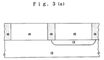
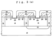
- Fig. 3 are cross-sectional views of a semiconductor device showing manufacturing process thereof according to the embodiment of the present invention.
- Fig. 1 is a diagram showing the change of the thickness of oxide film formed on a silicon surface with time when a silicon substrate is immersed in ultra pure water containing 9 ppm oxygen by volume. The thickness of the oxide film was measured with an ESCA and an elipsometer. In Fig. 1, the thickness of the oxide film formed on the silicon substrate is plotted as ordinate, and the elapsed time after the substrate being immersed in ultra pure water at 23 °C is plotted as abscissa.
- the oxide film of 4.2 nm in thickness was formed after a silicon wafer had been placed in the pure water containing dissolved oxygen of 9 ppm for 46 days.
- Table 1 shows the thickness of the oxide film and bond energy between silicon and oxygen atoms in the oxide film after the oxide film of 4.2 nm in thickness which had been formed in the pure water was heated at 500 °C in oxygen gas or nitrogen gas atmosphere for 1 hour.
- bond energy shown in Table 1 are the difference of bond energy between an Si 2p peak of a silicon-oxygen bond and an Si 2p3/2 of a silicon-silicon bond in X-ray photoelectron spectrum.
- the thickness of the oxide film increased to 4.9 nm after the thermal treatment ( annealing ) in oxygen gas, and decreased slightly to 3.98 nm after the thermal treatment in nitrogen gas.
- the bond energy increased after the thermal treatment in both oxygen and nitrogen gas.
- the bond energy of the oxide film thus prepared is greater than that of the oxide film which is formed on the silicon surface in dry oxygen at 800 °C.
- an oxide film of more than 3 nm in thickness and large bond energy between silicon and oxygen atoms can be formed by the method; for example, by heating a silicon substrate in oxygen gas or nitrogen gas atmosphere after the substrate being immersed in pure water containing 9 vol. ppm oxygen.
- This oxide film can be used only in the case that electrode regions 29, 30, 31 are made of materials having high melting point such as Mo, W, Ta, Ti, Pd, or silicides of these metal.
- the present method can be applied to not only the case that the regions 29, 30, 31 are made of high melting point materials, but also to the case that the regions are made of Al. Furthermore, it is also possible to increase the bond energy to more than 4.64 eV by the present method.
- the aqueous solution in which oxygen and/or oxygen-containing molecule is dissolved used in the first step of the present invention, is an aqueous solution containing oxygen, an aqueous solution containing ozone, hydrogen peroxide, a sulfuric acid and hydrogen peroxide solution, a hydrogen chloride and hydrogen peroxide solution, or an ammonia and hydrogen peroxide solution for example.
- a solution in which oxygen is dissolved in hydrogen peroxide it is also possible to use a solution in which oxygen is dissolved in hydrogen peroxide.
- an oxide film is formed on a substrate by bringing a substrate surface in contact with a solution in which oxygen and/or oxygen-containing molecule is dissolved.
- a solution in which oxygen and/or oxygen-containing molecule is dissolved it is preferable because the formation rate of an oxide film is increased that the solution is brought into contact with a catalyst to accelerate the decomposition of the molecule contained in the solution. Therefore, when the substrate is brought in contact with the solution with dissolved oxygen of e.g. 0.1 vol ppm, the adoption of the catalyst makes it possible to use the solution with dissolved oxygen less than 0.1 vol. ppm at the beginning.
- a solid catalyst platinum is used.
- the contact of hydrogen peroxide with a platinum catalyst cause to generate oxygen radical from hydrogen peroxide, and as a result, the effect on the formation rate of an oxide film becomes remarkable.
- 1 nm thick oxide film is formed at room temperature in 30 minutes, and 2 to 5 nm thick film is formed at 70 to 85 °C in 24 hours.
- the oxide film used for e.g. gate oxide film of MOS LSI can be obtained in a short time to be put into practical application.
- the content of TOC in hydrogen peroxide is required to be less than 1 ppm and is preferable to be less than 0.1 ppm. Also in other solutions, impurities content less than 1ppm is desirable and less than 0.1 ppm is preferable.
- the oxidation film is formed on the silicon substrate surface in relatively short time, and the formation rate of the oxide film increases as the content of dissolved oxygen or oxygen-containing molecule increases .
- the solubility limit of oxygen is 14 ppm in aqueous solution at 0 °C and at atmospheric pressure
- the content of dissolved oxygen or oxygen-containing molecule can be increased by, e.g., immersing a silicon substrate into ultra pure water in a closed vessel, by introducing oxygen gas into the vessel, and then by increasing the pressure of oxygen.
- the upper limit value of 10000 vol. ppm is desirable as the content of oxygen and/or oxygen-containing molecule.
- the same oxygen-containing molecule as used in the first step can also be used in vapor phase.
- the inert gas is nitrogen gas, argon gas or helium gas for example. Oxygen, oxygen-containing molecule, inert gas or a mixture of them are also used.
- the formation rate of the oxide film increases remarkably.
- a temperature range of 20 to 600 °C is desirable and a range of 100 to 500 °C is preferable. Furthermore, the temperature close to 500 °C is better from the practical use point view because the film can be formed in shorter time.
- the temperature of thermal treatment in the second step is set to be as high as possible only if the wafer condition is allowed.
- the pressure of the atmosphere is not restricted; therefore any condition such as reduced pressure, atmospheric pressure or high pressure condition is available.
- Fig. 2 is a cross-sectional view of the semiconductor device according to the embodiment. Only one CMOS element of the semiconductor device is drawn in the figure.
- 11 is an electrode on back of a substrate
- 12 is a p+ substrate
- 13 is an n+ buried layer
- 14 is a p ⁇ high resistance region
- 15 is an n ⁇ high resistant region
- 16 is an isolation region
- 17 and 18 are n+ regions
- 19 and 20 are p+ regions
- 21, 22, 23, and 24 are metal silicide such as MOSi2, WSi2, TaSi2 or Pd2Si
- 25 and 26 are silicon oxide films (gate insulating film) formed in the same manner as mentioned previously
- 27 and 28 are gate electrodes
- 29, 30 and 31 are metal electrode such as Al, AlSi or AlCu
- 32, 33 and 34 are metal fluoride films for electrically separating electrodes 27, 28, 29 and 30; for example, AlF3 when Al is used as an electrode
- 35 is a PSG film or
- the interface between gate insulating film 25 and region 14 is formed deeper in the region 14 than those between regions 17, 18 and region 14.
- the interface between gate insulating film 26 and region 15 is also formed deeper in the region 15 than those between regions 19, 20 and region 15.
- the short-channel effect does not easily occur in this structure because the electric field between a source and a drain is weakened in the channel.
- gate electrodes 27, 28 are preferably made of material such as Al, AlSi or AlCu which has a large diffusion potential or built-in potential to both n+ region 17, 18 and p+ region 19, 20.
- Al has a diffusion potential or a bult-in potential of about 0.7 V to n+ region and of about 0.4 V to p+ region.
- the selected material of electrode is a matter of design choice provided that the work function of the electrode have a large barrier to both n+ region and p+ region. Thus, high melting point metals or metal silicides are also available. Therefore, the resistance of gate electrode is small.
- the diffusion potentials or built-in potentials of p+ substrate 12 and gate electrode 27 to n+ source region and those of n+ buried region 13 and gate electrode 28 to p+ source region produce potential barrier in the channel, and therefore normally-off characteristic of MOS transistor is attained at a low impurity concentration of 1014 to 1016 cm ⁇ 3 in channel regions 14, 15.
- the regions 14, 15 are of high resistance, and the concentration of impurities is maintained low.
- the channels which electrons or holes pass through are maintained wide and therefore a short channel is realized without causing decrease in mobility of carrier. Consequently, MOS transistor with large conversion conductance g m can be obtained.
- a junction plane between n+ region 17 and region 14, that between n+ region 18 and region 14, that between p+ region 19 and region 15, and that between p+ region 20 and region 15 are flat and of small area, resulting in the small fringe effect and small capacitance between a source region and a substrate, between a drain and a substrate and between a source region and a drain region.
- electrodes 29, 30, 31 are made of e.g. Al, AlSi, AlCu and AlCuSi and therefore resistance of source and drain electrodes are small. Because of small resistance of source, drain and gate, of small capacitance of a source and drain capacitor, and of large conversion conductance g m , the transistor has high speed performance characteristic. Metal such as Mo, W, Ta and Ti can also be used as a source and a drain electrode.
- semiconductor integrated circuit composed of a high speed insulated gate transistor can be realized.
- a p+ substrate 12 with a buried region 13 is used in Fig.2.
- insulator substrates such as sapphire, spinel, quartz, AlN or SiC are also available.
- Fig.3 shown is an example of manufacturing process of the semiconductor device shown in Fig. 2.
- explanation is made for the case that a p+ substrate is used as a substrate.
- n+ buried region is formed by diffusing P from a PSG film deposited on the region 13 of p+ substrate 12 by e.g. CVD method.
- the region 13 can also be formed by ion implantation of P or As and following annealing for activation.
- Isolation region 16, p ⁇ region 14 and n ⁇ region 15 are formed in the following manner. For example, after the thermal oxidation film of tens of nm thickness is formed on the surface of the substrate 12 having buried region 13, a PSG film or BPSG film of prescribed thickness is deposited. The portion corresponding to the region 14, 15 in the thermal oxidation film and PSG film or BPSG film is removed by reactive ion etching. Then, selective epitaxial film is formed on regions 14, 15 by the use of e.g. CVD method using SiH4, Si2H6 or SiH2Cl2
- Fig. 3(a) the structure shown in Fig. 3(a) is constructed.
- the manufacturing method is not restricted by that mentioned above, and the selected thickness of region 14, 15 is a matter of design choice. Thickness of 0.03 - 0.5 ⁇ m is typically selected.
- metal layer of 10 to 20 nm thickness such as W, Ta, Ti and Mo.
- As is implanted into region 14, and B and Si are implanted into region 15 through the metal layer by ion implantation. Thereafter annealing is carried out for activation.
- regions 21, 22, 23, 24 of metal silicide layer, n+ region 17, 18 and p+ region 19, 20 are formed as shown in Fig. 3(b).
- Al film of 0.2 to 1.0 ⁇ m thickness is deposited by sputtering or CVD and then prescribed portions are removed by reactive ion etching as shown in Fig. 3(c).
- regions 29, 30, 31 are fluorinated at e.g. 100 °C for 4 hours by using ultra pure F2 gas and then is annealed at 150 °C in inert gas such as nitrogen gas for 5 hours to form an insulator layer of AlF3 which is shown as region 32, 33, 34 on the Al surface in Fig.3(d).
- inert gas such as nitrogen gas
- contact holes are formed by etching prescribed portion of metal silicide, n+ region and p+ region. In this etching process, the regions 32, 33, 34 act as a mask.
- the oxide films are formed on the exposed surface inside the contact holes. Namely, the oxide films are formed at a temperature less than 500 °C on silicide layer, n+ region and p+ region, as shown in Fig.3(e).
- the semiconductor device shown in Fig. 2 is constructed.
- the present invention is also applied to the surface of any materials such as other semiconductors and metals as well as the surface of silicon.
- oxide film 1 Two pieces of silicon wafer were immersed in 30% hydrogen peroxide solution which was in contact with a platinum catalyst. After 1 hour, an oxide film of 7 A in thickness was formed on the silicon wafer. The oxide film thus formed was such that the difference of bonding energy between Si 2p peak due to a silicon-oxygen bond and Si 2p3/2 peak due to a silicon-silicon bond was 3.99 eV in X-ray photoelectron spectrum. This oxide film is described as the oxide film 1 hereinafter.
- One of two wafers on which the oxide film 1 had been formed was thermally treated at 800 °C for 1 hour in nitrogen gas containing impurities of less than several ppb. After this treatment, the thickness of the oxide film became 9 A and the difference of the bonding energy became 4.22 eV between Si 2p peak due to a silicon-oxygen bond and Si 2p3/2 peak due to silicon-silicon bond in X-ray photoelectron spectrum.
- the oxide film after the thermal treatment is described as the oxide film 2.
- Both the wafer with the oxide film 1 and that with the oxide film 2 were placed in the atmosphere containing hydrogen fluoride of 0.6 to 1.3 vol.% and moisture of 10 ⁇ 2 to 5 ppm.
- the oxide film 1 was easily removed but the oxide film 2 was not removed, indicating that the oxide film 2 can be used as a mask in etching process.
- An electric voltage of 1 V was applied to the oxide films 1 and 2.
- An electric current passing through the oxide films 1 was more than 1 A/cm2; on the other hand, a current passing through the oxide film 2 was less than 1 x 10 ⁇ 4 A/cm2.
- the film with the bonding energy difference between Si 2p peak and Si 2p3/2 peak of more than 4.1 eV has excellent dielectric strength.
- oxide film 2 to various insulator, e.g. gate insulating film, semiconductor device with excellent performance can be obtained. Furthermore, it is possible to decrease the thickness of insulator in various devices and use such film as, e.g. tunnel insulating film.
- the present invention it is possible to form an oxide film on a substrate surface at low temperature and at the same time to control the bond strength between oxygen and atoms constituting the substrate surface in the oxide film.
- the present invention having such a feature makes it possible to form an oxide film with a prescribed thickness of e.g. 0.5 to 10 nm at a low temperature of e.g. less than 600 °C and to increase the bond strength of oxygen and atoms constituting the surface of the substrate in the oxide film to the value larger than that in the oxide film formed by the thermal oxidation at high temperature.
- the method of the present invention can be carried out at a temperature close to room temperature, an oxide film is formed by using a reaction apparatus with simple structure. Thus, a high efficiency semiconductor device is manufactured at low cost as compared with the method where oxide film is formed at high temperature.
Landscapes
- Formation Of Insulating Films (AREA)
- Insulated Gate Type Field-Effect Transistor (AREA)
- Glass Compositions (AREA)
- Silicon Compounds (AREA)
- Chemically Coating (AREA)
Applications Claiming Priority (3)
| Application Number | Priority Date | Filing Date | Title |
|---|---|---|---|
| JP113958/89 | 1989-05-07 | ||
| JP11395889 | 1989-05-07 | ||
| PCT/JP1990/000581 WO1990013911A1 (fr) | 1989-05-07 | 1990-05-07 | Procede de formation d'une pellicule d'oxyde |
Publications (3)
| Publication Number | Publication Date |
|---|---|
| EP0471845A1 true EP0471845A1 (de) | 1992-02-26 |
| EP0471845A4 EP0471845A4 (en) | 1992-04-22 |
| EP0471845B1 EP0471845B1 (de) | 1995-11-15 |
Family
ID=14625472
Family Applications (1)
| Application Number | Title | Priority Date | Filing Date |
|---|---|---|---|
| EP90907409A Expired - Lifetime EP0471845B1 (de) | 1989-05-07 | 1990-05-07 | Verfahren zur herstellung eines siliziumoxydfilmes |
Country Status (7)
| Country | Link |
|---|---|
| US (1) | US5360768A (de) |
| EP (1) | EP0471845B1 (de) |
| JP (1) | JP3122125B2 (de) |
| KR (1) | KR920702020A (de) |
| AT (1) | ATE130466T1 (de) |
| DE (1) | DE69023644T2 (de) |
| WO (1) | WO1990013911A1 (de) |
Cited By (3)
| Publication number | Priority date | Publication date | Assignee | Title |
|---|---|---|---|---|
| EP0720213A3 (de) * | 1994-12-28 | 1997-05-07 | Matsushita Electronics Corp | Kondensator für integrierte Schaltung und Verfahren zu ihrer Herstellung |
| US6204111B1 (en) | 1994-12-28 | 2001-03-20 | Matsushita Electronics Corporation | Fabrication method of capacitor for integrated circuit |
| GB2370043A (en) * | 2000-12-12 | 2002-06-19 | Mitel Corp | Chemical treatment of silica films |
Families Citing this family (11)
| Publication number | Priority date | Publication date | Assignee | Title |
|---|---|---|---|---|
| JPH09251995A (ja) * | 1989-05-07 | 1997-09-22 | Tadahiro Omi | 絶縁酸化膜の形成方法 |
| JP3169114B2 (ja) * | 1995-05-29 | 2001-05-21 | 信越半導体株式会社 | 単結晶薄膜の製造方法 |
| KR980701134A (ko) * | 1995-10-26 | 1998-04-30 | 요트.게.아.롤페즈 | 반도체 장치 제조 방법(Method of Manufacturing a Semiconductor Device) |
| TW462093B (en) * | 1997-03-05 | 2001-11-01 | Hitachi Ltd | Method for manufacturing semiconductor integrated circuit device having a thin insulative film |
| KR100468665B1 (ko) * | 1997-05-16 | 2005-08-29 | 삼성전자주식회사 | 산화막형성방법 |
| JP3808975B2 (ja) * | 1997-06-17 | 2006-08-16 | 忠弘 大見 | 半導体製造用水分の発生方法 |
| JPH11283924A (ja) * | 1998-03-27 | 1999-10-15 | Super Silicon Kenkyusho:Kk | 半導体ウエハ製造方法 |
| US6644324B1 (en) | 2000-03-06 | 2003-11-11 | Cymer, Inc. | Laser discharge chamber passivation by plasma |
| JP4095326B2 (ja) | 2002-03-29 | 2008-06-04 | 株式会社東芝 | 半導体装置の製造方法及び半導体装置 |
| JP4164324B2 (ja) * | 2002-09-19 | 2008-10-15 | スパンション エルエルシー | 半導体装置の製造方法 |
| CN119742231A (zh) * | 2024-11-07 | 2025-04-01 | 北方集成电路技术创新中心(北京)有限公司 | 一种氧化层的制造方法及半导体器件 |
Family Cites Families (12)
| Publication number | Priority date | Publication date | Assignee | Title |
|---|---|---|---|---|
| DE1189655B (de) * | 1960-05-25 | 1965-03-25 | Siemens Ag | Verfahren zum Erzeugen einer stabilisierenden Oxydschicht auf einer Halbleiteroberflaeche |
| US3850687A (en) * | 1971-05-26 | 1974-11-26 | Rca Corp | Method of densifying silicate glasses |
| CA954426A (en) * | 1971-06-25 | 1974-09-10 | Robert E. Albano | Chemical growth of insulating layers on gallium arsenide |
| US3791862A (en) * | 1971-12-22 | 1974-02-12 | Bell Telephone Labor Inc | Chemical growth of insulating layers on gallium arsenide |
| US3852120A (en) * | 1973-05-29 | 1974-12-03 | Ibm | Method for manufacturing ion implanted insulated gate field effect semiconductor transistor devices |
| US3925107A (en) * | 1974-11-11 | 1975-12-09 | Ibm | Method of stabilizing mos devices |
| JPS51114875A (en) * | 1975-04-01 | 1976-10-08 | Mitsubishi Electric Corp | Semiconductor device manufacturing method |
| JPS5275181A (en) * | 1975-12-13 | 1977-06-23 | Sony Corp | Formation of oxide film |
| JPS5466075A (en) * | 1977-11-04 | 1979-05-28 | Mitsubishi Electric Corp | Manufacture of semiconductor device |
| JPS55121653A (en) * | 1979-03-14 | 1980-09-18 | Fujitsu Ltd | Method of treating surface of semiconductor substrate |
| JPS6329516A (ja) * | 1986-07-22 | 1988-02-08 | Mitsubishi Electric Corp | 半導体装置の製造方法 |
| US4784975A (en) * | 1986-10-23 | 1988-11-15 | International Business Machines Corporation | Post-oxidation anneal of silicon dioxide |
-
1990
- 1990-05-07 WO PCT/JP1990/000581 patent/WO1990013911A1/ja not_active Ceased
- 1990-05-07 DE DE69023644T patent/DE69023644T2/de not_active Expired - Fee Related
- 1990-05-07 US US07/784,434 patent/US5360768A/en not_active Expired - Fee Related
- 1990-05-07 KR KR1019910700023A patent/KR920702020A/ko not_active Ceased
- 1990-05-07 AT AT90907409T patent/ATE130466T1/de not_active IP Right Cessation
- 1990-05-07 JP JP02506699A patent/JP3122125B2/ja not_active Expired - Fee Related
- 1990-05-07 EP EP90907409A patent/EP0471845B1/de not_active Expired - Lifetime
Cited By (8)
| Publication number | Priority date | Publication date | Assignee | Title |
|---|---|---|---|---|
| EP0720213A3 (de) * | 1994-12-28 | 1997-05-07 | Matsushita Electronics Corp | Kondensator für integrierte Schaltung und Verfahren zu ihrer Herstellung |
| US5929475A (en) * | 1994-12-28 | 1999-07-27 | Matsushita Electronics Corp | Capacitor for integrated circuit and its fabrication method |
| US6204111B1 (en) | 1994-12-28 | 2001-03-20 | Matsushita Electronics Corporation | Fabrication method of capacitor for integrated circuit |
| US6214660B1 (en) | 1994-12-28 | 2001-04-10 | Matsushita Electronics Corporation | Capacitor for integrated circuit and its fabrication method |
| CN1075243C (zh) * | 1994-12-28 | 2001-11-21 | 松下电器产业株式会社 | 集成电路用电容元件及其制造方法 |
| US6468875B2 (en) | 1994-12-28 | 2002-10-22 | Matsushita Electric Industrial Co., Ltd. | Fabrication method of capacitor for integrated circuit |
| GB2370043A (en) * | 2000-12-12 | 2002-06-19 | Mitel Corp | Chemical treatment of silica films |
| US6537623B2 (en) | 2000-12-12 | 2003-03-25 | Dalsa Semiconductor Inc. | Manufacture of silica waveguides with minimal absorption |
Also Published As
| Publication number | Publication date |
|---|---|
| JP3122125B2 (ja) | 2001-01-09 |
| US5360768A (en) | 1994-11-01 |
| WO1990013911A1 (fr) | 1990-11-15 |
| EP0471845A4 (en) | 1992-04-22 |
| EP0471845B1 (de) | 1995-11-15 |
| ATE130466T1 (de) | 1995-12-15 |
| KR920702020A (ko) | 1992-08-12 |
| DE69023644D1 (de) | 1995-12-21 |
| DE69023644T2 (de) | 1996-04-18 |
Similar Documents
| Publication | Publication Date | Title |
|---|---|---|
| KR100202003B1 (ko) | 반도체 및 반도체기판표면의 산화막의 형성방법 | |
| EP0072603B1 (de) | Verfahren zur Herstellung einer Halbleiteranordnung mit einer Isolierschicht aus Siliziumdioxid, die mit einer Schicht aus Siliziumoxynitrid bedeckt ist | |
| US4378628A (en) | Cobalt silicide metallization for semiconductor integrated circuits | |
| US4266985A (en) | Process for producing a semiconductor device including an ion implantation step in combination with direct thermal nitridation of the silicon substrate | |
| KR100391840B1 (ko) | 반도체기판표면상의절연막형성방법및그형성장치 | |
| EP0471845B1 (de) | Verfahren zur herstellung eines siliziumoxydfilmes | |
| US5089432A (en) | Polycide gate MOSFET process for integrated circuits | |
| US3923559A (en) | Use of trapped hydrogen for annealing metal-oxide-semiconductor devices | |
| US5214305A (en) | Polycide gate MOSFET for integrated circuits | |
| US4105805A (en) | Formation of metal nitride oxide semiconductor (MNOS) by ion implantation of oxygen through a silicon nitride layer | |
| US5130266A (en) | Polycide gate MOSFET process for integrated circuits | |
| JP2692554B2 (ja) | 半導体装置の製造方法 | |
| JPH0234455B2 (de) | ||
| KR20040111683A (ko) | 실리콘 기재 표면의 이산화실리콘막 형성방법, 반도체기재 표면의 산화막 형성방법 및 반도체 장치의 제조방법 | |
| EP1540718A2 (de) | Methode zur herstellung und/oder modifizierung eines dielektrischen films auf einer halbleiteroberfläche | |
| JPWO1990013911A1 (ja) | 酸化膜の形成方法 | |
| KR20050094474A (ko) | 반도체 소자 제조 방법 | |
| EP0471844A1 (de) | Siliziumoxydfilm und halbleiteranordnung die diesen enthält | |
| US6579614B2 (en) | Structure having refractory metal film on a substrate | |
| EP0154670A2 (de) | Verfahren zur Herstellung einer Halbleiteranordnung mit einer Isolierschicht | |
| JPH10270434A (ja) | 半導体ウエーハの洗浄方法及び酸化膜の形成方法 | |
| JP3533377B2 (ja) | 半導体基板表面の酸化膜の形成方法及び半導体装置の製造方法 | |
| JPH1050701A (ja) | 半導体及び半導体基板表面の酸化膜の形成方法 | |
| JP3917282B2 (ja) | 半導体基板表面の絶縁膜の形成方法 | |
| JP3173757B2 (ja) | 半導体装置の作製方法 |
Legal Events
| Date | Code | Title | Description |
|---|---|---|---|
| PUAI | Public reference made under article 153(3) epc to a published international application that has entered the european phase |
Free format text: ORIGINAL CODE: 0009012 |
|
| 17P | Request for examination filed |
Effective date: 19911106 |
|
| AK | Designated contracting states |
Kind code of ref document: A1 Designated state(s): AT BE DE DK FR GB IT LU NL SE |
|
| A4 | Supplementary search report drawn up and despatched |
Effective date: 19920228 |
|
| AK | Designated contracting states |
Kind code of ref document: A4 Designated state(s): AT BE DE DK FR GB IT LU NL SE |
|
| 17Q | First examination report despatched |
Effective date: 19940614 |
|
| GRAA | (expected) grant |
Free format text: ORIGINAL CODE: 0009210 |
|
| AK | Designated contracting states |
Kind code of ref document: B1 Designated state(s): AT BE DE DK FR GB IT LU NL SE |
|
| PG25 | Lapsed in a contracting state [announced via postgrant information from national office to epo] |
Ref country code: IT Free format text: LAPSE BECAUSE OF FAILURE TO SUBMIT A TRANSLATION OF THE DESCRIPTION OR TO PAY THE FEE WITHIN THE PRE;WARNING: LAPSES OF ITALIAN PATENTS WITH EFFECTIVE DATE BEFORE 2007 MAY HAVE OCCURRED AT ANY TIME BEFORE 2007. THE CORRECT EFFECTIVE DATE MAY BE DIFFERENT FROM THE ONE RECORDED.SCRIBED TIME-LIMIT Effective date: 19951115 Ref country code: DK Effective date: 19951115 Ref country code: FR Effective date: 19951115 Ref country code: AT Effective date: 19951115 Ref country code: BE Effective date: 19951115 |
|
| REF | Corresponds to: |
Ref document number: 130466 Country of ref document: AT Date of ref document: 19951215 Kind code of ref document: T |
|
| REF | Corresponds to: |
Ref document number: 69023644 Country of ref document: DE Date of ref document: 19951221 |
|
| PG25 | Lapsed in a contracting state [announced via postgrant information from national office to epo] |
Ref country code: SE Effective date: 19960215 |
|
| EN | Fr: translation not filed | ||
| PG25 | Lapsed in a contracting state [announced via postgrant information from national office to epo] |
Ref country code: GB Effective date: 19960507 |
|
| PG25 | Lapsed in a contracting state [announced via postgrant information from national office to epo] |
Ref country code: LU Free format text: LAPSE BECAUSE OF NON-PAYMENT OF DUE FEES Effective date: 19960531 |
|
| PGFP | Annual fee paid to national office [announced via postgrant information from national office to epo] |
Ref country code: NL Payment date: 19960916 Year of fee payment: 7 |
|
| PLBE | No opposition filed within time limit |
Free format text: ORIGINAL CODE: 0009261 |
|
| STAA | Information on the status of an ep patent application or granted ep patent |
Free format text: STATUS: NO OPPOSITION FILED WITHIN TIME LIMIT |
|
| 26N | No opposition filed | ||
| GBPC | Gb: european patent ceased through non-payment of renewal fee |
Effective date: 19960507 |
|
| PG25 | Lapsed in a contracting state [announced via postgrant information from national office to epo] |
Ref country code: DE Effective date: 19970201 |
|
| PG25 | Lapsed in a contracting state [announced via postgrant information from national office to epo] |
Ref country code: NL Effective date: 19971201 |
|
| NLV4 | Nl: lapsed or anulled due to non-payment of the annual fee |
Effective date: 19971201 |