EP0464818A2 - Einrichtung und Verfahren zur Schätzung des abgetasteten Wertes der Impulsantwort und System zur Signalwiedergabe diese Einrichtung benutzend - Google Patents
Einrichtung und Verfahren zur Schätzung des abgetasteten Wertes der Impulsantwort und System zur Signalwiedergabe diese Einrichtung benutzend Download PDFInfo
- Publication number
- EP0464818A2 EP0464818A2 EP91111119A EP91111119A EP0464818A2 EP 0464818 A2 EP0464818 A2 EP 0464818A2 EP 91111119 A EP91111119 A EP 91111119A EP 91111119 A EP91111119 A EP 91111119A EP 0464818 A2 EP0464818 A2 EP 0464818A2
- Authority
- EP
- European Patent Office
- Prior art keywords
- decision
- generating
- signal
- operatively coupled
- equalized
- Prior art date
- Legal status (The legal status is an assumption and is not a legal conclusion. Google has not performed a legal analysis and makes no representation as to the accuracy of the status listed.)
- Withdrawn
Links
Images


Classifications
-
- H—ELECTRICITY
- H04—ELECTRIC COMMUNICATION TECHNIQUE
- H04L—TRANSMISSION OF DIGITAL INFORMATION, e.g. TELEGRAPHIC COMMUNICATION
- H04L7/00—Arrangements for synchronising receiver with transmitter
- H04L7/0054—Detection of the synchronisation error by features other than the received signal transition
- H04L7/0062—Detection of the synchronisation error by features other than the received signal transition detection of error based on data decision error, e.g. Mueller type detection
-
- H—ELECTRICITY
- H04—ELECTRIC COMMUNICATION TECHNIQUE
- H04L—TRANSMISSION OF DIGITAL INFORMATION, e.g. TELEGRAPHIC COMMUNICATION
- H04L25/00—Baseband systems
- H04L25/02—Details ; arrangements for supplying electrical power along data transmission lines
- H04L25/0202—Channel estimation
- H04L25/0212—Channel estimation of impulse response
Definitions
- the present invention generally relates to a device and method for estimating a sampled value of an impulse response. Such a device and method are used for a signal reproduction procedure in a digital transmission system. Further, the present invention is concerned with a signal reproduction system using such a device.
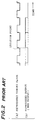
- FIG.1 is a block diagram of a conventional signal reproduction circuit used in a digital transmission system.
- the signal reproduction circuit is composed of a waveform equalizing circuit 101, a timing reproduction circuit 102, and a decision circuit 103.
- the waveform equalizing circuit 101 equalizes the waveform of a digital signal transmitted via an incoming line (reshaping function).
- the timing extraction circuit 102 reproduces a timing clock (retiming function) from an equalized (reshaped) digital signal output by the waveform equalizing circuit 101.
- the decision circuit 103 performs a decision procedure on the equalized digital signal by using the reproduced timing clock output by the timing reproduction circuit 102, and outputs a reproduced digital signal to an outgoing line (regeneration function).
- the timing reproduction circuit 102 generates the timing reproduction clock as shown in FIG.2(a) on the basis of an eye in, for example, an equalized AMI (Alternate Mark Inversion) output.
- the decision circuit 103 detects the mark or space of the equalized AMI output at each rise (decision point) of the reproduced timing clock, and generates a reproduced output (NRZ (Non Return to Zero) output), as shown in FIG.2(b).
- the timing reproduction circuit 102 is comprised of an analog circuit, as shown in FIG.3.
- the analog circuit shown in FIG.3 extracts a signal portion of the AMI waveform around only each peak value thereof by a full-wave rectification circuit 102-1.
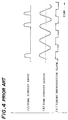
- a full-wave rectified output from the circuit 102-1 as shown in FIG.4(a) is input, via a resistor R, to an LC tank circuit 102-2, which is made up of an inductor L and a capacitor C.
- the LC tank circuit 102-2 generates a sine wave corresponding to a desired clock frequency, as shown in FIG.4(b).
- the sine wave output by the LC tank circuit 102-2 is shaped by a limiter amplifier 102-3, which generates the aforementioned reproduced timing clock, as shown in FIG.4(c).
- a timing reproduction circuit using a digital phase-locked loop has been proposed.
- a conventional DPLL is shown in FIG.5.
- the DPLL shown in FIG.5 is made up of a phase comparator 201, a frequency divider 202, and a master clock generator 203.
- the master clock generator 203 generates a master clock having a frequency (20.48MHz, for example) more than 100 times a necessary clock frequency (80kHz, for example).
- the frequency divider 202 divides the frequency of the master clock in order to generate a clock having the necessary clock frequency.
- the phase of the clock generated by the frequency divider 202 is compared with the phase of an input signal.
- the frequency dividing ratio in the frequency divider 202 is adjusted based on the phase difference between the signals input to the phase comparator 201.
- FIG.6 shows a signal reproduction circuit which uses a DPLL as described above.
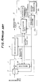
- the signal reproduction circuit shown in FIG.6 is composed of a waveform equalizing circuit 1, a timing reproduction circuit 2 and a decision circuit 3.
- the waveform equalizing circuit 1 is made up of an automatic gain controller (AGC) 11 and a decision feedback type equalizer 12.
- AGC automatic gain controller
- the AGC 11 receives an input signal in digital form and automatically adjusts the gain of the input signal to a fixed level.
- the equalizer 12 corrects the output of the AGC 11 on the basis of input and output signals of the decision circuit 3, as will be described in detail later.
- the timing reproduction circuit 2 generates a reproduced timing clock from an equalized signal output by the waveform equalizing circuit 1, and is composed of a sampled value estimating formula evaluation unit 21, a controller 22, a frequency divider 23 and a master clock generator 24.
- the evaluation unit 21 estimates an impulse response waveform of each isolated pulse contained in the input signal, and extracts information about the phase of the estimated impulse response waveform.
- the nth sampled value of the impulse response, labeled hn is estimated as follows: where fn is the nth value in a train of sampled values of the input signal (equalized outputs), and an-k is a train of decided values of the input signal.
- Formula (1) can be modified as follows:
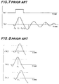
- FIG.7(a) shows an input pulse
- FIG.7(b) shows an impulse response thereof.
- the first sampled value h1 of the impulse response is estimated by the above-mentioned formula (4).
- a threshold value hth is determined.
- the sampling point is at a correct position, the first sampled value h1 is equal to the threshold value hth.
- the sampling point is positioned at a left shoulder portion of a main response contained in the impulse response.
- the difference between the first sampled value h1 and the threshold value hth is calculated.
- the sampled value h1 is larger than the threshold value hth, as shown in FIG.8(b)
- the sampling point is too delayed.
- the sampled value h1 is smaller than the threshold value hth, as shown in FIG.8(c)
- the sampling point is too advanced.
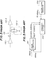
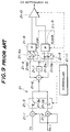
- FIG.9 is a block diagram of the sampled value estimating formula evaluation unit 21.
- the evaluation unit 21 is composed of multipliers 21-1 and 21-2, switches 21-3 - 21-5, an adder 21-6, a delay element (T) 21-7, registers 21-8 and 21-9, a comparator 21-10 and a controller 21-11.
- the multiplier 21-1 calculates the product fn ⁇ an-1 of the equalized output sample fn and the decided value sample an-1.
- the multiplier 21-2 calculates the square an-12 of the decided value sample an-1.
- the switch 21-3 has two switches 21-3a and 21-3b, which operate in opposite switching modes.
- the switch 21-3a controls the passage of the output fn ⁇ an-1 from the multiplier 21-1
- the switch 21-3b controls the passage of the output an-12 from the multiplier 21-2.
- the switches 21-4 and 21-5 are used for controlling the inputting of the values calculated by the adder 21-6 to the registers 21-8 and 21-9, respectively, and operates in the opposite switching modes.
- the switch 21-4 has two switches 21-4a and 21-4b, and the switch 21-5 has two switches 21-5a and 21-5b.
- the switch 21-3a and the switch 21-4 operate in the same switching mode, and the switch 21-3b and the switch 21-5 operate in the same switching mode.
- the adder 21-6 adds the (n-1)th calculated value and the (n-2)th calculated value.
- the delay element 21-7 delays the output of the adder 21-6 by a predetermined time.
- the register 21-8 is used for storing E[an-1 ⁇ fn], and the register 21-8 is used for storing E[an-12].
- the comparator 21-10 compares E[an-1 ⁇ fn] read out from the register 21-8 with E[an-12] read out from the register 21-9. It can be from the above that the circuit shown in FIG.9 uses the threshold value hth equal to 1.
- the controller 21-11 controls the comparison timing of the comparator 21-11, clears the registers 21-8 and 21-9, and controls the switches 21-3 - 21-5.
- the product fn ⁇ an-1 is calculated by the multiplier 21-1, and the square an-12 of the decided value an-1 is calculated by the multiplier 21-2.
- the switches 21-3a, 21-4a and 21-4b are closed first. Thereby, an updating value for calculating the average of fn ⁇ an-1 is stored in the register 21-8.
- the switches 21-3b, 21-5a and 21-5b are closed. Thereby, an updating value for calculating the average of an-12 is stored in the register 21-9.
- E[an-1 ⁇ fn] and E[an-12] respectively read out from the registers 21-8 and 21-9 are compared with each other by the comparator 21-10 in response to a control signal output by the controller 21-11.
- the comparator 21-10 outputs information indicating which E[an-1 ⁇ fn] or E[an-12] is greater (or smaller) than the other.
- the comparator 21-10 executes the above-mentioned comparing operation, the contents of the registers 21-8 and 21-9 are cleared.
- the evaluation unit 21 generates a control signal for adjusting the frequency dividing ratio in the frequency divider 23 on the basis of the comparison results output by the evaluation unit 21.
- the frequency divider 23 divides the frequency of a master clock generated by the master clock generator 24. The frequency dividing ratio is controlled by the control signal output by the controller 22.
- the clock signal output by the frequency divider 23 is input, as the reproduced timing clock, to the decision circuit 3, and is also input to the AGC 11, the equalizing circuit 12 and the evaluation unit 21.
- the decision circuit 3 shown in FIG.6 carries out the decision procedure on the equalized signal output by the waveform equalizing circuit 1 by using the timing reproduction signal output by the timing reproduction circuit 2, so that the reproduced digital signal can be generated.
- the timing reproduction circuit 2 estimates the impulse response waveform from the equalized output, and compares the estimated sampled value h1 with the threshold value hth in order to adjust the frequency dividing ratio.
- the frequency divider 23 outputs the reproduced timing clock to the decision circuit 3 in accordance with the adjusted frequency dividing ratio.
- the decision circuit 3 detects the mark or space of each equalized impulse response at a decision point (sampling point) which is at each rise of the reproduced timing clock, so that the reproduced output is generated by the decision circuit 3.
- a conventional system as described above has a disadvantage in that it is necessary to calculate the products an-1 ⁇ fn and an-12 in order to estimate the sampled value of each impulse response.
- the reproduction/repeater function can be implemented by a one-chip VLSI.
- the multiplier needs an extremely large scale integrated circuit having, for example, thousands of gates, each having a 16bit x 16bit scale.
- a more specific object of the present invention is to provide a device capable of estimating the sampled value of an impulse response without using a multiplier.
- a device for estimating a sampled value of an impulse response from input and output signals of a decision circuit which performs a signal decision procedure for reproducing a digital signal, the input signal having an equalized waveform comprising: first means, operatively coupled to the decision circuit, for generating a first average of absolute values of decided values obtained from the output signal of the decision circuit; second means, operatively coupled to the decision circuit, for generating a second average of absolute values of equalized outputs obtained from the input signal of the decision circuit; and third means, operatively coupled to the first and second means, for generating a ratio of the first average and the second average, the ratio being an estimate of the sampled value of the impulse response at a sampling point.
- a device for estimating a sampled value of an impulse response from input and output signals of a decision circuit which performs a signal decision procedure for reproducing a digital signal, the input signal having an equalized waveform comprising: first means, operatively coupled to the decision circuit, for generating a first sum of absolute values of j (j is a natural number) samples of decided values obtained from the output signal of the decision circuit; second means, operatively coupled to the decision circuit, for generating a second sum of absolute values of j samples of equalized outputs obtained from the input signal of the decision circuit; and third means, operatively coupled to the first and second means, for generating a ratio of the first sum and the second sum, the ratio being an estimate of the sampled value of the impulse response at a sampling point.
- first means operatively coupled to the decision circuit, for generating a first sum of absolute values of j (j is a natural number) samples of decided values obtained from the output signal of the decision circuit
- second means operatively coupled to the decision circuit, for generating
- Another object of the present invention is to provide a signal reproduction system using the aforementioned device.
- a signal reproduction system comprising: waveform equalizing means for equalizing a digital input signal transmitted via a transmission line and for generating an equalized input signal; decision means, operatively coupled to the waveform equalizing means, for performing a decision procedure for the equalized input signal at a predetermined timing and for generating a reproduced digital signal; and timing reproduction means, operatively coupled to the waveform equalizing means and the decision means, for generating a clock signal from the equalized input signal and the reproduced digital signal, the clock signal defining the predetermined timing of the decision means.
- the timing reproduction means comprises: first means, operatively coupled to the decision means, for generating a first average of absolute values of samples of decided values obtained from the reproduced digital signal output by the decision means; second means, operatively coupled to the decision means, for generating a second average of absolute values of samples of equalized outputs obtained from the equalized input signal input to the decision means; third means, operatively coupled to the first and second means, for generating a ratio of the first average and the second average, the ratio being estimated as the sampled value of an impulse response at a sampling point; and control means, operatively coupled to the third means, for comparing the sampled value output by the third means with a threshold value and for adjusting the timing of the clock signal on the basis of a result of comparison.
- control means for comparing the sampled value output by the third means with a threshold value and for adjusting a gain of the waveform equalizing means for equalizing the waveform of the digital input signal on the basis of a result of comparison.
- a signal reproduction system which has a timing reproduction means comprising: first means, operatively coupled to the decision circuit, for generating a first sum of absolute values of j (j is a natural number) samples of decided values obtained from the reproduced digital signal of the decision means; second means, operatively coupled to the decision circuit, for generating a second sum of absolute values of j samples of equalized outputs obtained from the equalized input signal of the decision means; third means, operatively coupled to the first and second means, for generating a ratio of the first sum and the second sum, the ratio being estimated as the sampled value of an impulse response at a sampling point; and control means, operatively coupled to the third means, for comparing the sampled value output by the third means with a threshold value and for adjusting the timing of the clock signal on the basis of a result of comparison.
- control means for comparing the sampled value output by the third means with a threshold value and for adjusting a gain of the waveform equalizing means for equalizing the waveform of the digital input signal on the basis of a result of comparison.
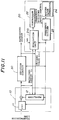
- FIG.10A shows an overview of a signal reproduction device according to a first preferred embodiment of the present invention.
- the signal reproduction device shown in FIG.10A is composed of a waveform equalizing circuit 10, a timing reproduction circuit 20 and a decision circuit 30.
- the waveform equalizing circuit 10 receives a digital input signal transmitted via a transmission line, and equalizes the waveform of the received digital input signal.
- the timing reproduction circuit 20 reproduces a timing clock from an equalized output signal from the waveform equalizing circuit 10 and a reproduced digital output signal from the decision circuit 30.
- a first sampled value estimating procedure or a second sampled value estimating procedure is used.
- the first sampled value estimating procedure calculates the ratio of the average of the absolute values of decided values obtained from the output signal of the decision circuit 30 and the average of the absolute values of equalized outputs (sampled values) obtained from the input signal of the decision circuit 30.
- the ratio thus calculated is estimated as the sampled value of the impulse response at the sampling point.
- the second sampled value estimating procedure calculates the ratio of the sum of the absolute values of j samples (j is a natural number) of decided values obtained from the output signal of the decision circuit 30 and the sum of the absolute values of j samples of equalized outputs (sampled values) obtained from the input signal of the decision circuit 30.
- the ratio thus calculated is an estimate of the sampled value of the impulse response at the sampling point.
- the timing reproduction circuit 20 compares the sampled value of the impulse response with a predetermined threshold value, and controls the timing for the decision procedure executed by the decision circuit 30. When the sampled value of the impulse response is greater than the threshold value, the sampling point is too advanced. On the other hand, when the sampled value of the impulse response is smaller than the threshold value, the sampling point is too delayed.
- the decision circuit 30 carries out the decision procedure for the equalized output in accordance with the timings indicated by the timing reproduction circuit 20.
- FIG.10B is a block diagram of an overview of a signal reproduction device according to a second preferred embodiment of the present invention.
- a gain controller 40 shown in FIG.10B is substituted for the timing reproduction circuit 20 shown in FIG.10A.
- the gain controller 40 controls the gain of the waveform equalizing circuit 10. More specifically, the gain controller 40 compares the sampled value calculated by either the aforementioned first or second sampled value estimating procedure with the threshold value, and controls the gain of the waveform equalizing circuit 10 on the basis of the comparison results. When the sampled value of the impulse response is greater than the threshold value, the gain controller 40 decreases the gain of the waveform equalizing circuit 10. On the other hand, when the sample value of the impulse response is smaller than the threshold value, the gain controller 40 increases the gain of the waveform equalizing circuit 10.
- the timing reproduction circuit 20 is substituted for the timing reproduction circuit 2 shown in FIG.6.
- the timing reproduction circuit 20 includes a sampled value estimating formula evaluation unit 210, which is substituted for the sampled value estimating formula evaluation unit 21 shown in FIG.6.
- An evaluation unit 210 estimates an impulse response waveform of each isolated (individual) pulse contained in the input signal, and extracts information about the phase thereof.
- the evaluation unit 210 estimates the impulse response hn in the following way.
- the equalized output sample (sampled value) fn is calculated as follows:
- the sign of each absolute value term in formula (5) is mainly determined at a sampling point near the peak value of the impulse response. Particularly, when the decision feedback starts to work, the sign in each absolute value term is definitely determined at the sampling point near the peak value of the impulse response. For example, if the second term of the formula (5) is close to the peak value, following formula (6) is obtained: where: where ( ⁇ ) means that the sign is determined at random.
- the sampled value of the impulse response at the sampling point is defined by the ratio of the average value E[
- the sampled value calculated in the above-mentioned way is compared with the threshold value hth.
- the sampled point is delayed.
- the sampled value h1 is larger than the threshold value hth, the sampled point is advanced. In this way, it is possible to always position the sampling point as shown in FIG.8(a).
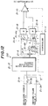
- FIG.12 is a block diagram of the sampled value estimating formula evaluation unit 210.
- the evaluation unit 210 has an absolute value calculation circuit 21-12 in addition to the aforementioned switches 21-3 - 21-5, the adder 21-6, the delay element 21-7, the registers 21-8 and 21-9, the comparator 21-10 and the controller 21-11. It should be noted that the evaluation unit 21 shown in FIG.12 does not have the multipliers 21-1 and 21-2 shown in FIG.9, but instead has the absolute value calculation circuit 21-12. The structural elements other than the absolute value calculation circuit 21-12 have been described.
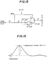
- FIG.13 is a block diagram of the absolute value calculation circuit 21-12, which is made up of a selector 21-121, a NOT gate 21-122 and an adder 21-123.
- the most significant bit MSB
- MSB serves as a switch signal for controlling the selector 21-121.
- the input data is inverted by the NOT gate 21-122, and +1 is added to an inverted version of the input data by the adder 21-123.
- the combination of the NOT gate 21-122 and the adder 21-123 generates the absolute value of a binary signal which is one bit of the input data. It will be noted that a plurality of combinations of the NOT gate 21-122 and the selector 21-123 are provided for the respective bits of the input data. However, only one combination is illustrated in FIG.13 for the sake of simplicity.
- the register 21-8 functions to store the average value E
- the register 21-9 functions to store the average value E
- the comparator 21-10 compares the output E
- the controller 21-11 controls the operating timing of the comparator 21-11, clears the registers 21-8 and 21-9, and controls the switches 21-3 - 21-5.
- the absolute value calculation circuit 21-12 calculates the absolute value of the sampled value fn of the equalized input signal. Then, an updating value for calculating E
- j) of the register 21-8 is compared with the output E
- the comparator 21-10 executes the comparing operation, the contents of the registers 21-8 and 21-9 are cleared.
- the first embodiment of the present invention does not need any multiplier.
- a compact evaluation unit which can easily be comprised of hardware. This means that it is not necessary to use a large-scale circuit, such as a digital signal processor.
- the threshold value hth is not limited to 1, but can be set to a desired value.
- the precursory method a rise of the impulse response from zero is detected and always regulated at zero.
- the aforementioned first or second sampled value estimating procedure is applied to an estimation of an equalized level of the signal via the transmission line.
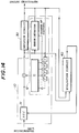
- FIG.14 is a block diagram of the second embodiment of the present invention, which is composed of the waveform equalizing circuit 10, the decision circuit 30 and the gain control circuit 40.
- the waveform equalizing circuit 10 is composed of the AGC 11 and the decision feedback type equalizer 12.
- the AGC 11 automatically controls the gain of the amplified signal so that it is always fixed to a predetermined level.
- the equalizer 12 corrects the output from the AGC 11 on the basis of the input and output signals of the decision circuit 30.
- the AGC 11 is controlled by a control signal generated and output by the gain control circuit 40, which is comprised of an evaluation unit as has been described previously.
- the gain control circuit 40 is referred to as the evaluation circuit 40.
- the equalizer 12 is comprised of delay elements, an error detector, weighting factor multipliers and a summation device, all of which are connected in a conventional way.
- the evaluation unit 40 operates in the same way as the evaluation unit 210 shown in FIG.11. That is, the evaluation unit 40 calculates the ratio of the average value E[
- the ratio thus calculated is an estimate of the sampled value h1 of the impulse response at the sampling point.
- the evaluation circuit 40 When the sampled value h1 of the impulse response is greater than the threshold value hth, the evaluation circuit 40 generates the control signal directed to reducing the gain of the AGC 11. On the other hand, when the sampled value h1 of the impulse response is smaller than the threshold value hth, the evaluation unit 40 generates the control signal directed to increasing the gain of the AGC 11. It should be noted that since the second embodiment operates in the precursory method, the sampled value h1 is positioned at the peak of the equalized output signal, as shown in FIG.15.
- the threshold value hth is set equal to, for example, 1.
- the second embodiment of the present invention has the same advantages as those of the first embodiment thereof. It should be noted that the second embodiment does not require any multiplier.
Landscapes
- Engineering & Computer Science (AREA)
- Computer Networks & Wireless Communication (AREA)
- Signal Processing (AREA)
- Power Engineering (AREA)
- Dc Digital Transmission (AREA)
- Filters That Use Time-Delay Elements (AREA)
- Cable Transmission Systems, Equalization Of Radio And Reduction Of Echo (AREA)
- Synchronisation In Digital Transmission Systems (AREA)
Applications Claiming Priority (2)
| Application Number | Priority Date | Filing Date | Title |
|---|---|---|---|
| JP2179152A JPH0468834A (ja) | 1990-07-05 | 1990-07-05 | インパルス応答の標本値推定方式 |
| JP179152/90 | 1990-07-05 |
Publications (2)
| Publication Number | Publication Date |
|---|---|
| EP0464818A2 true EP0464818A2 (de) | 1992-01-08 |
| EP0464818A3 EP0464818A3 (en) | 1993-05-05 |
Family
ID=16060868
Family Applications (1)
| Application Number | Title | Priority Date | Filing Date |
|---|---|---|---|
| EP19910111119 Withdrawn EP0464818A3 (en) | 1990-07-05 | 1991-07-04 | Device and method for estimating sampled value of impulse response and signal reproduction system using the device |
Country Status (4)
| Country | Link |
|---|---|
| US (1) | US5291522A (de) |
| EP (1) | EP0464818A3 (de) |
| JP (1) | JPH0468834A (de) |
| CA (1) | CA2046172A1 (de) |
Families Citing this family (3)
| Publication number | Priority date | Publication date | Assignee | Title |
|---|---|---|---|---|
| JPH06343085A (ja) * | 1993-04-07 | 1994-12-13 | Hitachi Ltd | 信号復調復号装置および信号復調復号方法 |
| TWI265700B (en) * | 2004-05-27 | 2006-11-01 | Samsung Electronics Co Ltd | Decision feedback equalization input buffer |
| US20100207669A1 (en) * | 2009-02-19 | 2010-08-19 | Ideacom Technology Corporation (Taiwan) | Freqeuncy adjusting apparatus and the method therefor |
Family Cites Families (18)
| Publication number | Priority date | Publication date | Assignee | Title |
|---|---|---|---|---|
| WO1981001089A1 (en) * | 1979-10-15 | 1981-04-16 | Western Electric Co | Control of coefficient drift for fractionally spaced equalizers |
| FR2482809B1 (fr) * | 1980-05-14 | 1986-11-14 | Labo Electronique Physique | Systeme adaptatif de reception de donnees numeriques a compensation des distorsions d'amplitude et de phase introduites par le canal de transmission des donnees |
| JPS5962228A (ja) * | 1982-10-01 | 1984-04-09 | Nec Corp | 自動等化器 |
| GB2134355B (en) * | 1983-01-12 | 1986-03-05 | Ncr Co | Circuit for reducing errors in a data receiver |
| US4564952A (en) * | 1983-12-08 | 1986-01-14 | At&T Bell Laboratories | Compensation of filter symbol interference by adaptive estimation of received symbol sequences |
| JPS60210032A (ja) * | 1984-04-03 | 1985-10-22 | Nec Corp | 自動等化装置 |
| US4599732A (en) * | 1984-04-17 | 1986-07-08 | Harris Corporation | Technique for acquiring timing and frequency synchronization for modem utilizing known (non-data) symbols as part of their normal transmitted data format |
| JPS6182545A (ja) * | 1984-08-29 | 1986-04-26 | Fujitsu Ltd | タイミング引込み方法 |
| JPS6211326A (ja) * | 1985-07-09 | 1987-01-20 | Hitachi Ltd | 自動等化器再設定方式 |
| JPS62292079A (ja) * | 1986-06-12 | 1987-12-18 | Toshiba Corp | 自動波形等化器 |
| US4815103A (en) * | 1987-10-29 | 1989-03-21 | American Telephone And Telegraph Company | Equalizer-based timing recovery |
| US4800573A (en) * | 1987-11-19 | 1989-01-24 | American Telephone And Telegraph Company | Equalization arrangement |
| JPH01185042A (ja) * | 1988-01-20 | 1989-07-24 | Fujitsu Ltd | タイミング再生方式 |
| JPH01240038A (ja) * | 1988-03-19 | 1989-09-25 | Fujitsu Ltd | ピーク値比較型タイミング再生方式 |
| JPH01240039A (ja) * | 1988-03-19 | 1989-09-25 | Fujitsu Ltd | ダブルサンプリング型タイミング再生方式 |
| JP2519301B2 (ja) * | 1988-08-19 | 1996-07-31 | 富士通株式会社 | タイミング再生回路 |
| JP2581765B2 (ja) * | 1988-06-27 | 1997-02-12 | 富士通株式会社 | タイミング再生回路 |
| CA1311033C (en) * | 1988-03-19 | 1992-12-01 | Shinji Ohta | Circuit for obtaining accurate timing information received signal |
-
1990
- 1990-07-05 JP JP2179152A patent/JPH0468834A/ja active Pending
-
1991
- 1991-07-03 US US07/725,610 patent/US5291522A/en not_active Expired - Fee Related
- 1991-07-04 EP EP19910111119 patent/EP0464818A3/en not_active Withdrawn
- 1991-07-04 CA CA002046172A patent/CA2046172A1/en not_active Abandoned
Also Published As
| Publication number | Publication date |
|---|---|
| EP0464818A3 (en) | 1993-05-05 |
| CA2046172A1 (en) | 1992-01-06 |
| JPH0468834A (ja) | 1992-03-04 |
| US5291522A (en) | 1994-03-01 |
Similar Documents
| Publication | Publication Date | Title |
|---|---|---|
| US6650699B1 (en) | Methods and apparatus for timing recovery from a sampled and equalized data signal | |
| US5216554A (en) | Digital phase error estimator | |
| US5406427A (en) | Clock generator for magnetic disk drive that switches between preamble and data portions | |
| EP0316459A1 (de) | Schnelle Takterfassung für Partial-Response-Signalisierung | |
| EP1039463B1 (de) | Signalverarbeitungsgerät | |
| JPH0777336B2 (ja) | 等化器におけるタツプ係数を調整する方法 | |
| US6289064B1 (en) | Synchronization equipment | |
| EP0469647A2 (de) | Entscheidungsrückgekoppelter Dekodierer mit Pipeline-Struktur | |
| US8027423B2 (en) | Synchronizing apparatus, synchronizing method, synchronizing program and data reproduction apparatus | |
| US5465059A (en) | Method and apparatus for timing acquisition of partial response class IV signaling | |
| JPH06334567A (ja) | 改善されたタイミング手段を有する受信機からなる送信方式 | |
| EP0464818A2 (de) | Einrichtung und Verfahren zur Schätzung des abgetasteten Wertes der Impulsantwort und System zur Signalwiedergabe diese Einrichtung benutzend | |
| JPH06103696A (ja) | データ信号再生装置 | |
| US5056121A (en) | Circuit for obtaining accurate timing information from received signal | |
| US5892474A (en) | Clock phase acquisition/tracking device and phase acquisition method | |
| JP2581765B2 (ja) | タイミング再生回路 | |
| JPH06152667A (ja) | クロック再生回路 | |
| JPH05135510A (ja) | 情報処理システム | |
| JPH0997476A (ja) | 自動等化器及びディジタル信号再生装置 | |
| JPH06231409A (ja) | 適応波形等化方式 | |
| JPH05252027A (ja) | 位相同期ループ回路 | |
| JP2002184125A (ja) | ディジタル信号再生装置 | |
| EP0566362A2 (de) | Adaptiver FIR-Entzerrer | |
| JPS63221733A (ja) | 受信装置 | |
| SU886262A1 (ru) | Устройство адаптивной коррекции межсимвольных искажений |
Legal Events
| Date | Code | Title | Description |
|---|---|---|---|
| PUAI | Public reference made under article 153(3) epc to a published international application that has entered the european phase |
Free format text: ORIGINAL CODE: 0009012 |
|
| AK | Designated contracting states |
Kind code of ref document: A2 Designated state(s): DE FR GB |
|
| PUAL | Search report despatched |
Free format text: ORIGINAL CODE: 0009013 |
|
| AK | Designated contracting states |
Kind code of ref document: A3 Designated state(s): DE FR GB |
|
| 17P | Request for examination filed |
Effective date: 19930517 |
|
| STAA | Information on the status of an ep patent application or granted ep patent |
Free format text: STATUS: THE APPLICATION HAS BEEN WITHDRAWN |
|
| 18W | Application withdrawn |
Withdrawal date: 19960926 |