EP0463545A2 - Substratvorspannungsgenerator für Halbleiteranordnungen - Google Patents
Substratvorspannungsgenerator für Halbleiteranordnungen Download PDFInfo
- Publication number
- EP0463545A2 EP0463545A2 EP91109989A EP91109989A EP0463545A2 EP 0463545 A2 EP0463545 A2 EP 0463545A2 EP 91109989 A EP91109989 A EP 91109989A EP 91109989 A EP91109989 A EP 91109989A EP 0463545 A2 EP0463545 A2 EP 0463545A2
- Authority
- EP
- European Patent Office
- Prior art keywords
- voltage
- well
- substrate bias
- pmos transistor
- substrate
- Prior art date
- Legal status (The legal status is an assumption and is not a legal conclusion. Google has not performed a legal analysis and makes no representation as to the accuracy of the status listed.)
- Granted
Links
Images
Classifications
-
- G—PHYSICS
- G11—INFORMATION STORAGE
- G11C—STATIC STORES
- G11C5/00—Details of stores covered by group G11C11/00
- G11C5/14—Power supply arrangements, e.g. power down, chip selection or deselection, layout of wirings or power grids, or multiple supply levels
-
- G—PHYSICS
- G11—INFORMATION STORAGE
- G11C—STATIC STORES
- G11C5/00—Details of stores covered by group G11C11/00
- G11C5/14—Power supply arrangements, e.g. power down, chip selection or deselection, layout of wirings or power grids, or multiple supply levels
- G11C5/145—Applications of charge pumps; Boosted voltage circuits; Clamp circuits therefor
- G11C5/146—Substrate bias generators
Definitions
- This invention relates to a substrate bias generator enclosed in a semiconductor integrated circuit device, such as a memory.
- a substrate voltage V BB in the order of -2 to -3.5V is supplied to a semiconductor substrate for effectively retaining data stored in memory cells.
- This substrate voltage V BB is set so as to be at a value lower than the ground voltage (0V) and is supplied to the substrate by a pumping operation by capacitors, as disclosed for example in Japanese Patent KOKAI (Laid-Open) Publication No. 1-154395(1989).
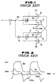
- Fig. 1 shows an example of the conventional substrate bias generator.
- An oscillator not shown, supplies anti-phase clock pulses by means of inverters 7 and 8 to a pair of capacitors 1 and 2, each formed by a pMOS transistor, so that these capacitors 1 and 2 will perform alternate charge-pumping operations.
- Rectifying pMOS transistors 3 and 4 are connected to a terminal P0 of the capacitor 1 and a terminal Q0 of the capacitor 2, respectively, while being connected in common to a mode 9 from which the substrate voltage V BB is outputted.
- a pair of pMOS transistors 5 and 6 for discharging to a grounding line, which is at 0V or at the GND level, are connected to the terminal P0 and Q0, respectively.
- the gate voltage of the pMOS transistor 5 is at the voltage level at the terminal Q0, so that the transistor 4 is turned off.
- the voltage level at the terminal P0 is raised by the current from the node 9 to a value in the vicinity of the substrate voltage V BB plus threshold voltage (V BB + Vth).
- V BB + Vth threshold voltage
- the voltage level at the terminal P0 is also raised so as to follow the voltage shift at the terminal R0.
- the pMOS transistor 3 is turned off, while the pMOS transistor 5 is turned on, as a result of which the voltage at the terminal P0 is again reset to close to the ground level.
- Such charge pumping operation occurs simultaneously with the capacitor 2 and the pMOS transistors 5 and 6, so that substrate charges are drained alternately from the node 9 by means of pMOS transistors 5 and 6 to maintain a predetermine value of the substrate voltage V BB .
- the n-well is connected to the terminal R0, as shown in Fig. 1, and is alternately supplied with the source voltage Vcc and the ground voltage GND.
- the voltage level at the node 9 is approximately -2 to -3V almost steadfastly, so that, during the turn-on period of the transistor 3, the N-well voltage becomes higher about 2 to 3V than the source voltage.
- the threshold voltage Vth of the pMOS transistor 3 is rased. Referring to Fig. 2, which is a waveform diagram of the circuit shown in Fig.
- a substrate bias generator comprising a substrate level detector for detecting the voltage level of a substrate, an oscillator operated in accordance with the results of detection by said substrate level detector, and a pumping circuit including a rectifying p-channel MOS transistor formed in an n-well which is maintained at a negative voltage level during pumping. Since the n-well is maintained at the negative voltage, the threshold voltage of the rectifying pMOS transistor may be prevented from increasing to enable a high efficiency charge pumping operation.
- a charge pumping circuit for the n-well in provided for maintaining the negative voltage level of the n-well in which the rectifying p-channel MOS transistor is formed.
- the charge pumping circuit for the well may be adapted to be driven by the same signals from the oscillator as those driving the pumping circuit.
- the parasitic capacity between the well and the MOS transistor may be used to effect the pumping operation.
- Fig. 1 is a circuit diagram of a pumping circuit in a conventional substrate bias circuit.
- Fig. 2 is a waveform diagram for illustrating the pumping operation by the circuit shown in Fig. 1.
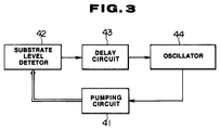
- Fig. 3 is a block diagram showing an embodiment of an overall substrate bias circuit according to the present invention.
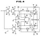
- Fig. 4 is a circuit diagram showing a concrete circuit arrangement of a pumping circuit of the substrate bias circuit shown in Fig. 3.
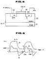
- Fig. 5 is a cross-sectional view of the portion of a semiconductor chip mounting rectifying pMOS transistors for illustrating the relation of the n-well and the rectifying pMOS transistors according to the present invention.
- Fig. 6 is a waveform diagram for illustrating the pumping operation performed by the substrate bias circuit shown in Fig. 4.
- a substrate bias generator according to a preferred embodiment of the present invention, employed in a dynamic RAM, is hereinafter explained by referring to Fig. 3.
- the substrate bias generator is constituted by a pumping circuit 41 for supplying a substrate voltage V BB by a charge pumping operation, a substrate level detector 42 for detecting whether the substrate voltage V BB is a predetermined voltage, a delay circuit 43 for delaying the signal indicating the result of detection, and an oscillator 43 adapted for starting its oscillation by a signal from the delay circuit 43.
- the substrate level detector 42 outputs a signal conforming to the result of detection. This signal is supplied by means of the delay circuit 43 composed for a multistage inverter to the oscillator 44 where rectangular wave signals of a predetermined frequency are generated.
- These rectangular wave signals are amplified and transmitted to a pumping circuit 41 as later described.
- the substrate voltage V BB at a predetermined voltage value is supplied to a substrate, not shown, on which a memory core of a dynamic memory and peripheral circuits are formed.
- the substrate level detector 42 detects such voltage decrease, so that oscillation at the oscillator 44 is brought to a stop by the signal from the detector 42.
- the pumping circuit 41 includes capacitors 11 and 12, each formed by a pMOS transistor. These capacitors are formed by connecting the source drain and channels regions of the pMOS transistors connected in common to form nodes R1 and S1 as one terminals, with gate side nodes P1 and Q1 as the other terminals. Rectangular wave signals, produced by the oscillator 44, are supplied to the nodes R1 and S1 of the capacitors 11 and 12 by means of amplifier-inverters.
- the rectangular wave signals are supplied to the node R1 of the capacitor 11 by means of a two-stage inverter consisting of an inverter composed of a pMOS transistor 17 and an nMOS transistor 18, and an inverter composed of a pMOS transistor 19 and an nMOS transistor 20.
- the rectangular wave signals are supplied to the node S1 of the capacitor 12 by means of a single-stage inverter consisting of an inverter composed of a pMOS transistor 21 and an nMOS transistor 22. Because of the difference in the number of inverter stages, rectangular wave signals which are antiphase with respect to each other are supplied to the nodes R1 and S1 of the capacitors 11 and 12, respectively.
- Rectifying pMOS transistor 13 and 14 are provided between the node P1 of the capacitor 11 and the node 27 outputting the substrate voltage V BB and between the node Q1 of the capacitor 12 and the node 27, respectively.
- One of the source or the drain of the pMOS transistor 13 is connected to the node P1 of the capacitor 11 and the other of the source or the drain of the transistor 13 is connected to the node 27.
- One of the source or the drain of the pMOS transistor 14 is connected to the node Q1 of the capacitor 12 and the other of the source or the drain of the transistor 14 is connected to the node 27.
- the gate of the pMOS transistor 13 is connected to the node P1 and to the gate of the pMOS transistor 16.
- the gate of the pMOS transistor 14 is connected to the node Q1 and to the gate of the pMOS transistor 15. Since the gates of the pMOS transistors 13 and 14 are connected to their drains, the transistors 13 and 14 act as rectifiers. It is noted that these pMOS transistors 13 and 14 are each formed in an n-well. Due to the parasitic capacity C S as later described, the n-well is maintained at a negative voltage to prevent the threshold voltage from increasing.
- One of the source or the drain of the pMOS transistor 15 is connected to the node P1, while the gate of the pMOS transistor 15 is connected to the node Q1.
- One of the source or the drain of the pMOS transistor 16 is connected to the node Q1, while the gate of the pMOS transistor 16 is connected to the gate P1.
- the other of the source or the drain of each of the pMOS transistors 15 and 16 is supplied with the ground voltage GND.
- the voltages at the nodes R1 and S1 are supplied to the wells of the pMOS transistors 15 and 16.
- the pMOS transistor 15 and 16 function as resetting transistors for discharging the electrical charges at the nodes P1 and Q1 to grounding lines supplying the grounding voltage GND to clamp or reset the nodes P1 and Q1 at the grounding voltage GND.
- pMOS transistors 23 to 26 are connected to n-wells X1 and Y1 of the pMOS transistors 13 and 14, so that the n-wells X1 and Y1 are maintained at the negative voltage by these pMOS transistors 23 to 26.
- the grounding voltage GND is supplied to one of the source or the drain of each of the pMOS transistors 23 to 26.
- To the n-well X1 of the pMOS transistor 13 are connected the other of the source or the drain of the pMOS transistor 23, the gate of the pMOS transistor 24 and the gate as well as the other of the source or the drain of the pMOS transistor 25.
- n-well Y1 of the pMOS transistor 14 To the n-well Y1 of the pMOS transistor 14 are connected the other of the source or the drain of the pMOS transistor 24, the gate of the pMOS transistor 23 and the gate as well as the other of the source or the drain of the pMOS transistor 26.
- the well or the substrate, in which the channel of the pMOS transistor 23 is formed, is supplied with the voltage at the node R1
- the well or substrate, in which the channel of the pMOS transistor 24 is formed is supplied with the voltage at the node S1.
- n-wells X1 and Y1 are maintained at the negative voltages due to the parasitic capacities C S proper to these n-wells.
- an n-well 32 is formed on the n-type semiconductor substrate 31, and n-type impurity diffusion regions 33 and 34 are formed on the n-well 32 in isolation from each other.
- a gate electrode 35 in formed on a region between these p-type impurity diffusion regions 33 and 34 by the interposition of a gate insulating film, not shown.
- the n-well 32 becomes the n-well X1 or Y1 in Fig. 4.
- the parasitic capacity is formed at the junction between the n-well and each of the p type impurity diffusion regions 33 and 34.
- the n-well 32 is affected by voltage changes at the nodes P1 and Q1, due to capacitive coupling by the parasitic capacity C S between the region 33 and the n-well 32. More specifically, as a result of the coupling by the parasitic capacity C S , the n-well 32 acts as if it were driven by signals from the oscillator 44.
- the node R1 is at the "H" level which is the Vcc level approximately equal to 5V, while the node P1 of the capacitor 11 is approximately at the grounding voltage GND, because the pMOS transistor 15 is in the current-conducting state.
- the node S1 on the opposite side is at the "L" level or GND level approximately equal to 0V, whereas the node Q1 is at a level lower than the GND level, such as at -V BB -Vth1, where Vth1 is the threshold voltage of each of the pMOS transistors 13 and 14.
- the n-well X1 is at a level close to the GND level.
- the voltage level at node R1 shifts from the "H” level to the "L” level or GND level, approximately equal to 0V, by the signal from the oscillator 44. Then, by the capacitive coupling of the capacitor 11 by the pMOS transistor, the voltage level at the node P1 is lowered from the level of the grounding voltage GND, such that, at time t2, the voltage level at the node P1 falls to a level close to, for example, -5V, at time t2.
- the n-well X1 follows the voltage level decrease at the node P1, on account of the capacitive coupling due to the parasitic capacity C S between the n-well and the node P1.
- the voltage level at the n-well X1 shifts from the level close to the GND level to the negative level, as shown by a dotted line in Fig. 6.
- the pMOS transistor 24 With the n-well X1 thus shifted to the negative voltage level, the pMOS transistor 24 is in the current-conducting state, while the voltage level at the opposite side n-well Y1 is clamped or reset to the grounding voltage GND, even though it is raised under the influence of the parasitic capacity C S of the pMOS transistor 14.
- the pMOS transistor 23 Since the gate voltage of the pMOS transistor 23 is not in excess of the threshold voltage Vth, the pMOS transistor 23 is in the turn-off state, so that the grounding voltage GND is not supplied at this stage to the n-well X1 by means of the pMOS transistor 23. Thus the n-well X1 is maintained at the negative voltage level.
- the pMOS transistor 25, acting as a diode, is in the current-conducting state when the voltage level at the n-well X1 exceeds the threshold voltage Vth of the pMOS transistor 25.
- the pMOS transistor 25 functions to prevent the voltage level at the n-well X1 from decreasing excessively to prevent the forward current from flowing from the p-type semiconductor substrate towards the n-well X1 as a consequence of the excessive decrease of the voltage level at the n-well X1. It will be noted that the forward current tends to destruct DRAM data.
- the threshold voltage Vth1 of the pMOS transistor 13 is decreased in a manner as will be explained subsequently.
- the state of the pMOS transistor 13 at time t2 when the voltage level at the node P1 is lowered to a level close to -5V, the voltage level at the node P1 is supplied to the gate of the transistor 13, so that the transistor is turned on and hence the current may flow from the node 27 towards the node P1.
- the substrate voltage V BB is lowered.
- the voltage level at the node P1 With the current flowing towards the node P1, the voltage level at the node P1 is raised.
- the state of the pMOS transistor 13 is changed from the current-conducting or turn-on state to the turn-off state.
- the threshold voltage Vth1 of the pMOS transistor 13 has a small value, because the n-well X1 is maintained at the negative voltage, as explained hereinabove. That is, since the voltage difference between the level at the n-well X1 and the substrate voltage V BB is small, it becomes possible to prevent the threshold voltage from increasing. Thus, for the same voltage level at the node P1, a larger current is allowed to flow through the pMOS transistor 13 and more charges may be carried off from the node 27 in proportion to the reduction in the threshold voltage Vth1.
- the voltage level at the node R1 shifts at the next time t3 from the "L" level to the "H” level.
- the voltage level at the node P1 capacitively coupled to the node R1 also shifts by a value equal to the source voltage Vcc from the negative level which is equal to the substrate voltage V BB less the threshold voltage Vth1 or -(V BB + Vth1).
- the pMOS transistor 13 continues to be turned off and the pMOS transistor 15 is turned on, so that the voltage level at the node P1 is changed towards the grounding level GND until it is reset to the state shown at time t0.
- the potential at the n-well X1 is slightly raised to the positive side, with rise in voltage level at the node P1, due to the capacitive coupling in the pMOS transistor 13.
- the n-well Y1 is maintained at this time at the negative voltage due to the capacitive coupling of the pMOS transistor 14.
- the pMOS transistor 23, the gate voltage of which is the voltage level at the n-well Y1 is rendered conductive, so that the n-well X1 is discharged immediately so as to be maintained at or near the grounding voltage GND.
- the pumping circuit repeats the above described sequence of operations to supply the predetermined substrate voltage V BB from the node 27.
- the n-well of the rectifying pMOS transistor is maintained during its operation at the negative voltage, the threshold voltage Vth of the transistor may be lowered for improving the pumping efficiency of the pumping circuit.
- the substrate voltage V BB may be at a lower value in proportion to the reduction of the threshold voltage of the rectifying pMOS transistor to improve data retention properties.
Landscapes
- Engineering & Computer Science (AREA)
- Power Engineering (AREA)
- Semiconductor Integrated Circuits (AREA)
- Dram (AREA)
Applications Claiming Priority (2)
| Application Number | Priority Date | Filing Date | Title |
|---|---|---|---|
| JP2164289A JP2805991B2 (ja) | 1990-06-25 | 1990-06-25 | 基板バイアス発生回路 |
| JP164289/90 | 1990-06-25 |
Publications (3)
| Publication Number | Publication Date |
|---|---|
| EP0463545A2 true EP0463545A2 (de) | 1992-01-02 |
| EP0463545A3 EP0463545A3 (en) | 1993-10-27 |
| EP0463545B1 EP0463545B1 (de) | 1997-09-03 |
Family
ID=15790279
Family Applications (1)
| Application Number | Title | Priority Date | Filing Date |
|---|---|---|---|
| EP91109989A Expired - Lifetime EP0463545B1 (de) | 1990-06-25 | 1991-06-18 | Substratvorspannungsgenerator für Halbleiteranordnungen |
Country Status (5)
| Country | Link |
|---|---|
| US (1) | US5172013A (de) |
| EP (1) | EP0463545B1 (de) |
| JP (1) | JP2805991B2 (de) |
| KR (1) | KR100213304B1 (de) |
| DE (1) | DE69127515T2 (de) |
Cited By (4)
| Publication number | Priority date | Publication date | Assignee | Title |
|---|---|---|---|---|
| FR2689340A1 (fr) * | 1992-03-30 | 1993-10-01 | Samsung Electronics Co Ltd | Circuit de pompage de charge pour un générateur de tension de substrat dans un dispositif de mémoire à semi-conducteur. |
| EP0822477A3 (de) * | 1996-07-29 | 1998-04-01 | Townsend and Townsend and Crew LLP | Ladungspumpenschaltung für ein Halbleiter-Substrat |
| EP1028363A1 (de) * | 1996-07-29 | 2000-08-16 | Townsend and Townsend and Crew LLP | Ladungspumpenschaltung für ein Halbleiter-Substrat |
| EP0830686B1 (de) * | 1995-06-07 | 2003-09-10 | Intel Corporation | Spannungsschaltkreis für negative spannungen |
Families Citing this family (21)
| Publication number | Priority date | Publication date | Assignee | Title |
|---|---|---|---|---|
| JPH057149A (ja) * | 1991-06-27 | 1993-01-14 | Fujitsu Ltd | 出力回路 |
| KR940003301B1 (ko) * | 1991-12-20 | 1994-04-20 | 주식회사 금성사 | Ce버스 심볼 엔코딩 처리회로 |
| US5412257A (en) * | 1992-10-20 | 1995-05-02 | United Memories, Inc. | High efficiency N-channel charge pump having a primary pump and a non-cascaded secondary pump |
| EP0626750B1 (de) * | 1992-11-18 | 1997-09-24 | Oki Electric Industry Company, Limited | Leistungsversorgungs-spannungerhöher |
| KR960003219B1 (ko) * | 1993-04-16 | 1996-03-07 | 삼성전자주식회사 | 반도체 집적회로의 중간전위 발생회로 |
| JP2560983B2 (ja) * | 1993-06-30 | 1996-12-04 | 日本電気株式会社 | 半導体装置 |
| US5386151A (en) * | 1993-08-11 | 1995-01-31 | Advanced Micro Devices, Inc. | Low voltage charge pumps using p-well driven MOS capacitors |
| EP0696839B1 (de) * | 1994-08-12 | 1998-02-25 | Co.Ri.M.Me. Consorzio Per La Ricerca Sulla Microelettronica Nel Mezzogiorno | Spannungserhöher vom Ladungspumpentype |
| JPH09293789A (ja) * | 1996-04-24 | 1997-11-11 | Mitsubishi Electric Corp | 半導体集積回路 |
| JP4109340B2 (ja) * | 1997-12-26 | 2008-07-02 | 株式会社ルネサステクノロジ | 半導体集積回路装置 |
| US6285243B1 (en) | 2000-02-23 | 2001-09-04 | Micron Technology, Inc. | High-voltage charge pump circuit |
| US6801076B1 (en) | 2000-04-28 | 2004-10-05 | Micron Technology, Inc. | High output high efficiency low voltage charge pump |
| US6833752B2 (en) * | 2000-04-28 | 2004-12-21 | Micron Technology, Inc. | High output high efficiency low voltage charge pump |
| US6404270B1 (en) * | 2000-11-28 | 2002-06-11 | Cypress Semiconductor Corp. | Switched well technique for biasing cross-coupled switches or drivers |
| US6646493B2 (en) * | 2001-08-14 | 2003-11-11 | Micron Technology, Inc. | Voltage charge pump with circuit to prevent pass device latch-up |
| US6577552B2 (en) | 2001-08-30 | 2003-06-10 | Micron Technology, Inc. | Apparatus and method for generating an oscillating signal |
| DE60207190D1 (de) * | 2002-03-29 | 2005-12-15 | St Microelectronics Srl | Basisstufe für Ladungspumpeschaltung |
| JP2006101671A (ja) * | 2004-09-30 | 2006-04-13 | Fujitsu Ltd | 整流回路 |
| US7855592B1 (en) | 2006-09-28 | 2010-12-21 | Cypress Semiconductor Corporation | Charge pump |
| US10352986B2 (en) | 2016-05-25 | 2019-07-16 | United Microelectronics Corp. | Method and apparatus for controlling voltage of doped well in substrate |
| CN115864830B (zh) * | 2023-02-15 | 2023-06-02 | 深圳通锐微电子技术有限公司 | 负压除二转换电路和设备终端 |
Family Cites Families (11)
| Publication number | Priority date | Publication date | Assignee | Title |
|---|---|---|---|---|
| US4322675A (en) * | 1980-11-03 | 1982-03-30 | Fairchild Camera & Instrument Corp. | Regulated MOS substrate bias voltage generator for a static random access memory |
| JPS57199335A (en) * | 1981-06-02 | 1982-12-07 | Toshiba Corp | Generating circuit for substrate bias |
| NL8402764A (nl) * | 1984-09-11 | 1986-04-01 | Philips Nv | Schakeling voor het opwekken van een substraatvoorspanning. |
| US4670670A (en) * | 1984-10-05 | 1987-06-02 | American Telephone And Telegraph Company At&T Bell Laboratories | Circuit arrangement for controlling threshold voltages in CMOS circuits |
| JPS6266656A (ja) * | 1985-09-19 | 1987-03-26 | Toshiba Corp | 基板電位生成回路 |
| DE8714849U1 (de) * | 1986-12-23 | 1987-12-23 | Jenoptik Jena Gmbh, Ddr 6900 Jena | Geregelter CMOS-Substratspannungsgenerator |
| KR890005159B1 (ko) * | 1987-04-30 | 1989-12-14 | 삼성전자 주식회사 | 백 바이어스 전압 발생기 |
| US4794278A (en) * | 1987-12-30 | 1988-12-27 | Intel Corporation | Stable substrate bias generator for MOS circuits |
| IT1221261B (it) * | 1988-06-28 | 1990-06-27 | Sgs Thomson Microelectronics | Moltiplicatore di tensione omos |
| JPH0817033B2 (ja) * | 1988-12-08 | 1996-02-21 | 三菱電機株式会社 | 基板バイアス電位発生回路 |
| JP2780365B2 (ja) * | 1989-08-14 | 1998-07-30 | 日本電気株式会社 | 基板電位発生回路 |
-
1990
- 1990-06-25 JP JP2164289A patent/JP2805991B2/ja not_active Expired - Lifetime
-
1991
- 1991-06-15 KR KR1019910009908A patent/KR100213304B1/ko not_active Expired - Lifetime
- 1991-06-18 DE DE69127515T patent/DE69127515T2/de not_active Expired - Lifetime
- 1991-06-18 EP EP91109989A patent/EP0463545B1/de not_active Expired - Lifetime
- 1991-06-25 US US07/720,736 patent/US5172013A/en not_active Expired - Lifetime
Cited By (9)
| Publication number | Priority date | Publication date | Assignee | Title |
|---|---|---|---|---|
| FR2689340A1 (fr) * | 1992-03-30 | 1993-10-01 | Samsung Electronics Co Ltd | Circuit de pompage de charge pour un générateur de tension de substrat dans un dispositif de mémoire à semi-conducteur. |
| EP0830686B1 (de) * | 1995-06-07 | 2003-09-10 | Intel Corporation | Spannungsschaltkreis für negative spannungen |
| US6323721B1 (en) | 1996-07-26 | 2001-11-27 | Townsend And Townsend And Crew Llp | Substrate voltage detector |
| EP0822477A3 (de) * | 1996-07-29 | 1998-04-01 | Townsend and Townsend and Crew LLP | Ladungspumpenschaltung für ein Halbleiter-Substrat |
| US6064250A (en) * | 1996-07-29 | 2000-05-16 | Townsend And Townsend And Crew Llp | Various embodiments for a low power adaptive charge pump circuit |
| EP1028363A1 (de) * | 1996-07-29 | 2000-08-16 | Townsend and Townsend and Crew LLP | Ladungspumpenschaltung für ein Halbleiter-Substrat |
| US6137335A (en) * | 1996-07-29 | 2000-10-24 | Townsend And Townsend And Crew Llp | Oscillator receiving variable supply voltage depending on substrate voltage detection |
| US6323722B1 (en) | 1996-07-29 | 2001-11-27 | Townsend And Townsend And Crew Llp | Apparatus for translating a voltage |
| US6326839B2 (en) | 1996-07-29 | 2001-12-04 | Townsend And Townsend And Crew Llp | Apparatus for translating a voltage |
Also Published As
| Publication number | Publication date |
|---|---|
| US5172013A (en) | 1992-12-15 |
| DE69127515D1 (de) | 1997-10-09 |
| KR100213304B1 (ko) | 1999-08-02 |
| EP0463545B1 (de) | 1997-09-03 |
| EP0463545A3 (en) | 1993-10-27 |
| JP2805991B2 (ja) | 1998-09-30 |
| KR920001847A (ko) | 1992-01-30 |
| DE69127515T2 (de) | 1998-04-02 |
| JPH0462868A (ja) | 1992-02-27 |
Similar Documents
| Publication | Publication Date | Title |
|---|---|---|
| EP0463545B1 (de) | Substratvorspannungsgenerator für Halbleiteranordnungen | |
| KR100214407B1 (ko) | 고측부 스위치용 전하 펌프 회로 | |
| US6329869B1 (en) | Semiconductor device with less influence of noise | |
| JP3159749B2 (ja) | 集積回路 | |
| EP0653760B1 (de) | Spannungserhöhungsschaltung | |
| US4378506A (en) | MIS Device including a substrate bias generating circuit | |
| KR890005159B1 (ko) | 백 바이어스 전압 발생기 | |
| US5343088A (en) | Charge pump circuit for a substrate voltage generator of a semiconductor memory device | |
| US4581546A (en) | CMOS substrate bias generator having only P channel transistors in the charge pump | |
| US4691304A (en) | Semiconductor device having an arrangement for preventing operational errors | |
| US4820936A (en) | Integrated CMOS circuit comprising a substrate bias voltage generator | |
| JP3281984B2 (ja) | 基板電圧発生回路 | |
| EP0202074A1 (de) | Vorspannungsgeneratorkreis | |
| EP0055136A2 (de) | Halbleiterpufferschaltung | |
| EP0638984A1 (de) | Niederspannungsladungspumpe | |
| US4443720A (en) | Bootstrap circuit | |
| US6175263B1 (en) | Back bias generator having transfer transistor with well bias | |
| JPS62190746A (ja) | 基板バイアス発生回路 | |
| US6657903B2 (en) | Circuit for generating power-up signal | |
| JPH0993114A (ja) | レベル変換回路、内部電位発生回路および内部電位発生ユニット、半導体装置およびトランジスタ製造方法 | |
| US5343087A (en) | Semiconductor device having a substrate bias generator | |
| KR900006192B1 (ko) | 백 바이어스 전압 발생기 | |
| KR100432985B1 (ko) | 상승된출력전압을발생시키기위한회로 | |
| KR960006378B1 (ko) | 기판전압발생회로의 차아지펌프회로 | |
| US5313111A (en) | Substrate slew circuit providing reduced electron injection |
Legal Events
| Date | Code | Title | Description |
|---|---|---|---|
| PUAI | Public reference made under article 153(3) epc to a published international application that has entered the european phase |
Free format text: ORIGINAL CODE: 0009012 |
|
| AK | Designated contracting states |
Kind code of ref document: A2 Designated state(s): DE FR GB |
|
| PUAL | Search report despatched |
Free format text: ORIGINAL CODE: 0009013 |
|
| AK | Designated contracting states |
Kind code of ref document: A3 Designated state(s): DE FR GB |
|
| 17P | Request for examination filed |
Effective date: 19940324 |
|
| 17Q | First examination report despatched |
Effective date: 19960322 |
|
| GRAG | Despatch of communication of intention to grant |
Free format text: ORIGINAL CODE: EPIDOS AGRA |
|
| GRAH | Despatch of communication of intention to grant a patent |
Free format text: ORIGINAL CODE: EPIDOS IGRA |
|
| GRAH | Despatch of communication of intention to grant a patent |
Free format text: ORIGINAL CODE: EPIDOS IGRA |
|
| GRAA | (expected) grant |
Free format text: ORIGINAL CODE: 0009210 |
|
| AK | Designated contracting states |
Kind code of ref document: B1 Designated state(s): DE FR GB |
|
| REF | Corresponds to: |
Ref document number: 69127515 Country of ref document: DE Date of ref document: 19971009 |
|
| ET | Fr: translation filed | ||
| PLBE | No opposition filed within time limit |
Free format text: ORIGINAL CODE: 0009261 |
|
| STAA | Information on the status of an ep patent application or granted ep patent |
Free format text: STATUS: NO OPPOSITION FILED WITHIN TIME LIMIT |
|
| 26N | No opposition filed | ||
| REG | Reference to a national code |
Ref country code: GB Ref legal event code: IF02 |
|
| PGFP | Annual fee paid to national office [announced via postgrant information from national office to epo] |
Ref country code: FR Payment date: 20100706 Year of fee payment: 20 |
|
| PGFP | Annual fee paid to national office [announced via postgrant information from national office to epo] |
Ref country code: GB Payment date: 20100618 Year of fee payment: 20 Ref country code: DE Payment date: 20100625 Year of fee payment: 20 |
|
| REG | Reference to a national code |
Ref country code: DE Ref legal event code: R071 Ref document number: 69127515 Country of ref document: DE |
|
| REG | Reference to a national code |
Ref country code: DE Ref legal event code: R071 Ref document number: 69127515 Country of ref document: DE |
|
| REG | Reference to a national code |
Ref country code: GB Ref legal event code: PE20 Expiry date: 20110617 |
|
| PG25 | Lapsed in a contracting state [announced via postgrant information from national office to epo] |
Ref country code: GB Free format text: LAPSE BECAUSE OF EXPIRATION OF PROTECTION Effective date: 20110617 |
|
| PG25 | Lapsed in a contracting state [announced via postgrant information from national office to epo] |
Ref country code: DE Free format text: LAPSE BECAUSE OF EXPIRATION OF PROTECTION Effective date: 20110619 |