EP0460263A1 - Lineare CMOS-Ausgangsstufe - Google Patents
Lineare CMOS-Ausgangsstufe Download PDFInfo
- Publication number
- EP0460263A1 EP0460263A1 EP90110765A EP90110765A EP0460263A1 EP 0460263 A1 EP0460263 A1 EP 0460263A1 EP 90110765 A EP90110765 A EP 90110765A EP 90110765 A EP90110765 A EP 90110765A EP 0460263 A1 EP0460263 A1 EP 0460263A1
- Authority
- EP
- European Patent Office
- Prior art keywords
- transistor
- current
- output
- source
- cmos
- Prior art date
- Legal status (The legal status is an assumption and is not a legal conclusion. Google has not performed a legal analysis and makes no representation as to the accuracy of the status listed.)
- Granted
Links
- 230000000295 complement effect Effects 0.000 claims abstract description 16
- 239000003990 capacitor Substances 0.000 claims description 2
- 230000001105 regulatory effect Effects 0.000 claims description 2
- 230000003321 amplification Effects 0.000 description 6
- 238000003199 nucleic acid amplification method Methods 0.000 description 6
- 230000001419 dependent effect Effects 0.000 description 3
- 239000008186 active pharmaceutical agent Substances 0.000 description 1
- 238000006243 chemical reaction Methods 0.000 description 1
- 238000010586 diagram Methods 0.000 description 1
- 230000000694 effects Effects 0.000 description 1
- 230000005669 field effect Effects 0.000 description 1
- 238000005259 measurement Methods 0.000 description 1
Images

Classifications
-
- H—ELECTRICITY
- H03—ELECTRONIC CIRCUITRY
- H03F—AMPLIFIERS
- H03F3/00—Amplifiers with only discharge tubes or only semiconductor devices as amplifying elements
- H03F3/30—Single-ended push-pull [SEPP] amplifiers; Phase-splitters therefor
-
- H—ELECTRICITY
- H03—ELECTRONIC CIRCUITRY
- H03F—AMPLIFIERS
- H03F1/00—Details of amplifiers with only discharge tubes, only semiconductor devices or only unspecified devices as amplifying elements
- H03F1/32—Modifications of amplifiers to reduce non-linear distortion
- H03F1/3217—Modifications of amplifiers to reduce non-linear distortion in single ended push-pull amplifiers
-
- H—ELECTRICITY
- H03—ELECTRONIC CIRCUITRY
- H03F—AMPLIFIERS
- H03F3/00—Amplifiers with only discharge tubes or only semiconductor devices as amplifying elements
- H03F3/30—Single-ended push-pull [SEPP] amplifiers; Phase-splitters therefor
- H03F3/3001—Single-ended push-pull [SEPP] amplifiers; Phase-splitters therefor with field-effect transistors
Definitions
- the amplification of output stages in push-pull technology is generally dependent both on the signal frequency and more or less on the modulation. In extreme cases, the so-called takeover distortions result in the case of small modulations, particularly in B mode.
- the gain-dependent gain can have a disadvantageous effect on the processing of audio, measurement or other signals if attention is to be paid to the lowest possible distortion.
- Such changes in the amplification of the output stage for example, make the effective degree of negative feedback of operational amplifiers dependent on the control, so that the exact linearity over the entire control range is not guaranteed.
- CMOS output stages to combine quadratic characteristics of a complementary field-effect transistor pair with one another in such a way that the amplification of the output stage becomes independent of the modulation.
- the quadratic current-voltage characteristic curve is used for this an n and a p-channel transistor used.
- I DS drain-source current
- U GS gate-source voltage
- U T constant transistor threshold value
- ß transistor slope parameter.
- the complementary pair of transistors is driven at the respective gate connection by a common control potential, the source connection of the respective transistor being at a first or second fixed potential.
- control potential is generated in a preliminary stage, which is described in the article as a complementary cascode stage using differential technology.
- a disadvantage of the known circuit arrangement is that the internally generated fixed potential is only stabilized via an arrangement of complementary diodes and a source follower and is therefore not sufficiently low-resistance.
- CMOS output stage according to the invention is part of a larger monolithically integrated circuit arrangement in which only one supply voltage is to be used, which should be as low as possible for power dissipation reasons.
- FIG. 1 shows the circuit diagram of an operational amplifier with the CMOS output stage according to the invention.
- the FIG. Shows a CMOS output stage k which operates in A / B push-pull operation and which is controlled via a control line st with a control potential ud from a preliminary stage d.
- the entire arrangement represents a CMOS operational amplifier, the preliminary stage d of which is designed as a conventional input differential stage.
- the input of the CMOS output stage k is formed by the control line st, which is connected to the gate terminal of the first transistor n1 and to the gate terminal of the complementary second transistor p1. Both transistors form the complementary transistor pair kt, the output currents of which are connected to one another via a current mirror arrangement and a current differential stage, which supplies the output differential current id at an output terminal vo.
- the first transistor n1 also serves as the first Push-pull output transistor of the CMOS output stage, while the complementary second push-pull output transistor pa is connected to the drain terminal of the second transistor p1 via the current mirror arrangement described.
- the high-resistance current difference stage is formed by the drain connection node, which is identical to the output terminal v0 of the CMOS output stage k.
- the source connection of the first transistor n1 is connected to the first fixed potential u1, which is, for example, identical to the ground connection.
- the source connection of the second transistor p1 is connected to the second fixed potential u2, the level of which lies between the ground potential and the positive supply voltage Up, and is generated internally.
- the operating point and the design of the reference voltage source allow the operating point of the first and second transistors n1, p1 of the complementary transistor pair kt to be simulated, so that the reference potential at the input terminal of the reference voltage source corresponds exactly to the required second fixed potential u2.
- the source connection of the second Transistor p1 is fed with a low impedance with the reference potential.
- This enables the compensation circuit K via a first and a second current mirror c1, c2 as follows: The drain connection of the second transistor p1 is led to the input of the first current mirror c1, which is complementary to the conductivity type of the second transistor p1.
- the control potential ud is at its idle value - the second output transistor p2 always supplies the same amount of current as the constant current source q. No compensation current therefore flows through the compensation line r.
- the compensation circuit K is formed in a very simple manner from an addition to the current difference stage. Current amplification by a factor of 3 takes place between the second push-pull output transistor pa and the input of the second current mirror. Because at the zero level the drain currents of the two Push-pull output transistors n1, pa must be the same in opposite directions, it follows that at the zero control level, the drain current of the first transistor n1 is six times the drain current of the second transistor p1.
- the slopes of the two complementary transistors n1, p1 therefore differ by a second ratio, namely by a factor of 6. In the case of any other current conversion of the two current mirrors c1, c2, the slopes differ accordingly.
- Preferred ratio values are: 1 to 3 for the first and 3 to 10 for the second ratio.
- CMOS output stage k In the CMOS output stage k according to the figure are of the p-channel conduction type: the second transistor p1, the one reference diode pd and the transistors of the second current mirror c2 and the constant current source q.
- the n-channel conduction type the first transistor n1, the second reference diode nd and the transistors of the first current mirror c1.
- the preliminary stage d shown in the figure is a simple differential amplifier stage in CMOS technology. It contains a p-channel differential amplifier transistor pair tp, the common source connection of which is fed from the positive supply voltage Up via a p-channel input current source eq. The input differential voltage is fed to a first and a second gate terminal d1, d2.
- the drain connections of the differential amplifier-transistor pair tp are each led via a p-channel cascode transistor, the respective drain connection of which with the input or output of an n-channel input current mirror ec, which serves as an "active load", connected is.
- the output of the active load supplies the control line st with the control potential ud.
- An integrated MOS capacitor is used for internal frequency feedback c switched from the output terminal vo to a connection node v in the preliminary stage d.
- the connection node v lies between the cascode transistor at which the control potential ud is tapped and the drain terminal of the differential amplifier transistor pair tp connected to this cascode transistor.
- the preliminary stage d is supplied with a first and a second auxiliary potential u3, u4, with which the input current source eq or the cascode transistors are fixed in their operating point.
- the entire slope of the CMOS output stage k can be set as desired in addition to the described current amplification of the two current mirrors c1, c2, in particular via the constant current ik supplied by the constant current source q.
- the ratio of the output differential current id to the control potential ud on the input side is to be regarded as the slope.
- the CMOS output stage k can also advantageously be used as a transconductance amplifier with a slope which can be set as desired.
- the respective slope is directly proportional to the value of the variable control current iv.
- the signal to be regulated in amplitude is to be connected to the control line st as control potential ud.
- An analog multiplier can be implemented in the same way.
Landscapes
- Engineering & Computer Science (AREA)
- Power Engineering (AREA)
- Physics & Mathematics (AREA)
- Nonlinear Science (AREA)
- Amplifiers (AREA)
Abstract
Description
- Die Verstärkung von Ausgangsstufen in Gegentakttechnik ist im allgemeinen sowohl von der Signalfrequenz als auch mehr oder weniger von der Aussteuerung abhängig. Im Extremfall ergeben sich bei kleinen Aussteuerungen, insbesondere im B-Betrieb, die sogenannten Übernahmeverzerrungen. Die aussteuerungsabhängige Verstärkung kann sich nachteilig auf die Verarbeitung von Audio-, Meß- oder sonstiger Signale auswirken, wenn dabei auf möglichst geringe Verzerrungen geachtet werden soll. Durch derartige Verstärkungsänderungen der Ausgangsstufe wird beispielsweise der wirksame Gegenkopplungsgrad von Operationsverstärkern aussteuerungsabhängig, so daß die exakte Linearität über den gesamten Aussteuerungsbereich nicht gewährleistet bleibt.
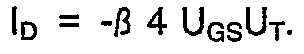
- Aus IEEE Journal of Solid-State Circuits, Bd.SC-22, Nr.6, Dezember 1987, Seite 1082-1089, insbesondere Seite 1085 mit der Fig.6a und der Fig.6b, ist es bekannt, bei CMOS-Ausgangsstufen die quadratischen Kennlinien eines komplementären Feldeffekt-Transistorpaares so miteinander zu kombinieren, daß die Verstärkung der Ausgangsstufe aussteuerungsunabhängig wird. Hierzu wird die quadratische Strom-Spannungskennlinie


IDS = Drain-Source-Strom, UGS = Gate-Source-Spannung, UT = konstanter Transistor-Schwellenwert, ß = Transistor-Steilheitsparameter. Das komplementäre Transistorpaar wird dabei am jeweiligen Gate-Anschluß von einem gemeinsamen Steuerpotential angesteuert, wobei der Source-Anschluß des jeweiligen Transistors auf einem ersten bzw. zweiten Festpotential liegt. Die Lage dieser Festpotentiale wird dabei so gewählt, daß beide Transistoren im gesamten Aussteuerungsbereich die jeweilige quadratische Strom-Spannungskennlinie nicht verlassen, also in ihrem jeweiligen Sättigungsbereich bleiben. Man spricht daher auch von einem A/B-Gegentaktbetrieb. Indem die beiden Ausgangsströme des komplementären Transistorpaares über eine Stromspiegelanordnung auf eine Stromdifferenzstufe geführt werden, wird dort hochohmig ein Differenzstrom erzeugt, der den gewünschten aussteuerungsunabhängigen proportionalen Stromverlauf aufweist. Mittels eines Lastwiderstandes kann dieser Differenzstrom in ein Spannungssignal umgewandelt werden, beispielsweise bei einem Operationsverstärker. - Durch die gemeinsame Ansteuerung des komplementären Transistorpaares wird der Drain-Strom des einen Transistors verkleinert und der des anderen Transistors vergrößert. Die folgende vereinfachte Darstellung veranschaulicht die strenge Proportionalität des Differenzstroms ID als Funktion der jeweiligen Gate-Source-Ansteuerspannung UGS:


- Die Erzeugung des Steuerpotentials erfolgt in einer Vorstufe, die in dem angegebenen Aufsatz als komplementäre Kaskodestufe in Differenztechnik ausgeführt ist.
- Als Nachteil erweist sich bei der bekannten Schaltungsanordnung, daß das intern erzeugte Festpotential lediglich über eine Anordnung aus komplementären Dioden und einem Source-Folger stabilisiert ist, und daher nicht ausreichend niederohmig ist.
- Es ist daher Aufgabe der in den Ansprüchen gekennzeichneten Erfindung, eine verbesserte CMOS-Ausgangsstufe für den A/B-Gegentaktbetrieb anzugeben, deren internes Festpotential lastunabhängiger ist.
- Neben der eigentlichen Lösung der Aufgabe erweist sich als weiterer Vorteil der Erfindung, daß die erforderliche Versorgungsspannung gegenüber der bekannten Schaltungsanordnung verkleinert werden kann, weil die Anzahl der in Reihe geschalteten Source-Drain-Strecken reduziert ist. Dies erweist sich als Vorteil, wenn die CMOS-Ausgangsstufe nach der Erfindung Teil einer größeren monolithisch integrierten Schaltungsanordnung ist, bei der nur eine Versorgungsspannung verwendet werden soll, die aus Verlustleistungsgründen möglichst niedrig sein soll.
- Die Erfindung und weitere Vorteile werden nun anhand der Figur näher erläutert, die das Schaltbild eines Operationsverstärkers mit der CMOS-Ausgangsstufe nach der Erfindung zeigt.
- Die Fig. zeigt eine CMOS-Ausgangsstufe k die im A/B-Gegentaktbetrieb arbeitet und die über eine Steuerleitung st mit einem Steuerpotential ud aus einer Vorstufe d angesteuert ist. Die gesamte Anordnung stellt einen CMOS-Operationsverstärker dar, dessen Vorstufe d als konventionelle Eingangs-Differenzstufe ausgebildet ist.
- Der Eingang der CMOS-Ausgangsstufe k wird durch die Steuerleitung st gebildet, die mit dem Gateanschluß des ersten Transistors n1 und mit dem Gateanschluß des dazu komplementären zweiten Transistors p1 verbunden ist. Beide Transistoren bilden das komplementäre Transistorpaar kt, dessen Ausgangsströme über eine Stromspiegelanordnung und eine Stromdifferenzstufe gegeneinander geschaltet sind, die an einer Ausgangsklemme vo den Ausgangsdifferenzstrom id liefert. Der erste Transistor n1 dient auch als erster Gegentaktausgangstransistor der CMOS-Ausgangsstufe, während der dazu komplementäre zweite Gegentaktausgangstransistor pa über die beschriebene Stromspiegelanordnung mit dem Drain-Anschluß des zweiten Transistors p1 verbunden ist.
- Durch den Drain-Verbindungsknoten, der mit der Ausgangsklemme v0 der CMOS-Ausgangsstufe k identisch ist, wird die hochohmige Stromdifferenzstufe gebildet. Der Source-Anschluß des ersten Transistors n1 ist mit dem ersten Festpotential u1 verbunden, das beispielsweise mit dem Masseanschluß identisch ist. Der Source-Anschluß des zweiten Transistors p1 ist mit dem zweiten Festpotential u2 verbunden, dessen Pegel zwischen dem Massepotential und der positiven Versorgungsspannung Up liegt, und intern erzeugt wird.
- Das zweite Festpotential u2 ergibt sich aus dem gewählten Arbeitspunkt des ersten und zweiten Transistors n1, p1, und zwar aus der Summe ihrer Gate-Source-Spannungen (= UGS). Diese werden in einer Referenzspannungsquelle nachgebildet, die aus der Serienschaltung eines n- und eines p-Kanal-Transistors gebildet ist. Beide Transistoren sind jeweils als Diode geschaltet. Der Fußpunkt der mit dem konstanten Strom ik gespeisten Referenzspannungsquelle ist mit dem ersten Festpotential u1 verbunden und der Eingangsanschluß liegt am Ausgang einer Konstantstromquelle q. Durch den Arbeitspunkt und die Auslegung der Referenzspannungsquelle kann der Arbeitspunkt des ersten und zweiten Transistors n1, p1 des komplementären Transistorpaares kt nachgebildet werden, so daß das Referenzpotential am Eingangsanschluß der Referenzspannungsquelle genau dem erforderlichen zweiten Festpotential u2 entspricht.
- Mittels einer Kompensationsschaltung K, die aus einer Strom-Mitkopplungsschleife (= "Bootstrapping"-Schaltung) besteht, wird erreicht, daß der Source-Anschluß des zweiten Transistors p1 niederohmig mit dem Referenzpotential gespeist wird. Dies ermöglicht die Kompensationsschaltung K über einen ersten und einen zweiten Stromspiegel c1, c2 wie folgt: Der Drain-Anschluß des zweiten Transistors p1 ist auf den Eingang des ersten Stromspiegels c1 geführt, der komplementär zum Leitungstyp des zweiten Transistors p1 ist. Der Ausgang des ersten Stromspiegels c1, der einen Stromverstärkungsfaktor (= erster Verhältniswert) vom Wert 2 aufweist, ist auf den Eingang des zweiten Stromspiegels c2 geschaltet, dessen erster Ausgangstransistor der zweite Gegentaktausgangstransistor pa ist und dessen zweiter Ausgangstransistor p2 Teil der Regelschaltung R ist. Der Drain-Anschluß dieses zweiten Ausgangstranistors p2, der zugleich eine Stromuntersetzung im Verhältnis 2 zu 1 bewirkt, ist gemeinsam mit dem Source-Anschluß des zweiten Transistors p1 und über eine Ausgleichsleitung r mit dem Eingangsanschluß der Referenzspannungsquelle verbunden. Im Ruhezustand - das Steuerpotential ud liegt auf seinem Ruhewert - liefert der zweite Ausgangstransistor p2 die stets genauso viel Strom wie die Konstantstromquelle q. Durch die Ausgleichsleitung r fließt somit kein Ausgleichsstrom. Ändert sich das Potential am Source-Anschluß des zweiten Transistors p1, dann fließt über die Ausgleichsleitung r ein Ausgleichsstrom, der einen gleichgroßen Kompensationsstrom im Ausgang der Kompensationsschaltung K (im Transistor p2) bewirkt, und den Ausgleichsstrom dadurch kompensiert. Durch den Kompensationsstrom wird das ursprüngliche zweite Festpotential u2 somit wiederhergestellt.
- Die Kompensationsschaltung K ist auf sehr einfache Weise aus einer Ergänzung der Stromdifferenzstufe gebildet. Zwischen dem zweiten Gegentaktausgangstransistor pa und dem Eingang des zweiten Stromspiegels findet eine Stromverstärkung um den Faktor 3 statt. Da im Aussteuerungsnullpunkt die Drain-Ströme der beiden Gegentaktausgangstransistoren n1, pa einander entgegengesetzt gleich sein müssen, folgt, daß im Aussteuerungsnullpunkt der Drainstrom des ersten Transistors n1 sechsmal so groß wie der Drainstrom des zweiten Transistors p1 ist. Die Steilheiten der beiden komplementären Transistoren n1, p1 unterscheiden sich also um einen zweiten Verhältniswert nämlich um den Faktor 6. Bei einer an sich beliebigen anderen Stromübersetzung der beiden Stromspiegel c1, c2 unterscheiden sich die Steilheiten entsprechend. Bevorzugte Verhältniswerte sind: 1 bis 3 für den ersten und 3 bis 10 für den zweiten Verhältniswert.
- In der CMOS-Ausgangsstufe k nach der Figur sind vom p-Kanal-Leitungstyp: der zweite Transistor p1, die eine Referenzdiode pd und die Transistoren des zweiten Stromspiegels c2 sowie der Konstantstromquelle q. Vom n-Kanal-Leitungstyp sind: der erste Transistor n1, die zweite Referenzdiode nd und die Transistoren des ersten Stromspiegels c1.
- Die in der Figur dargestellte Vorstufe d ist eine einfache Differenzverstärkerstufe in CMOS-Technik. Sie enthält ein p-Kanal-Differenzverstärker-Transistorpaar tp, dessen gemeinsamer Source-Anschluß über eine p-Kanal-Eingangsstromquelle eq aus der positiven Versorgungsspannung Up gespeist ist. Einem ersten und einem zweiten Gate-Anschluß d1, d2 wird die Eingangs-Differenzspannung zugeführt. Die Drain-Anschlüsse des Differenzverstärker-Transistorpaares tp sind jeweils über einen p-Kanal-Kaskodetransistor geführt, dessen jeweiliger Drain-Anschluß mit dem Ein- bzw. Ausgang eines n-Kanal-Eingangs-Stromspiegels ec, der als "aktive Last" dient, verbunden ist. Der Ausgang der aktiven Last speist die Steuerleitung st mit dem Steuerpotential ud. Zur internen Frequenzgegenkopplung ist ein mitintegrierter MOS-Kondensator c von der Ausgangsklemme vo auf einen Verbindungsknoten v in der Vorstufe d geschaltet. Der Verbindungsknoten v liegt zwischen dem Kaskodetransistor, an dem das Steuerpotential ud abgegriffen wird, und dem mit diesem Kaskodetransistor verbundenen Drain-Anschluß des Differenzverstärker-Transistorpaares tp. Ferner sind der Vorstufe d ein erstes und ein zweites Hilfspotential u3, u4 zugeführt, mit der die Eingangsstromquelle eq bzw. die Kaskodetransistoren in ihrem Arbeitspunkt festgelegt werden.
- Statt der in der Figur dargestellten Vorstufe d können auch andere Schaltungen verwendet werden, beispielsweise die angesprochene komplementäre Kaskodestufe.
- Die gesamte Steilheit der CMOS-Ausgangsstufe k ist außer über die beschriebene Stromverstärkung der beiden Stromspiegel c1, c2, insbesondere über den von der Konstantstromquelle q gelieferten konstanten Strom ik beliebig einstellbar. Als Steilheit ist dabei das Verhältnis von Ausgangsdifferenzstrom id und eingangsseitigem Steuerpotential ud anzusehen. Wird die Konstantstromquelle q durch einen variablen Steuerstrom iv ersetzt, dann kann die CMOS-Ausgangsstufe k auch mit Vorteil als Transkonduktanzverstärker mit beliebig einstellbarer Steilheit verwendet werden. Die jeweilige Steilheit ist direkt proportional zum Wert des variablen Steuerstromes iv. Das in der Amplitude zu regelnde Signal ist als Steuerpotential ud an die Steuerleitung st anzuschließen. In gleicher Weise ist ein analoger Multiplizierer realisierbar.
Claims (8)
- CMOS-Ausgangsstufe, die im A/B-Gegentaktbetrieb arbeitet und die über eine Steuerleitung (st) mit einem Steuerpotential (ud) aus einer Vorstufe (d) angesteuert ist,- die Steuerleitung (st) speist die Gate-Anschlüsse eines komplementären Transistorpaares (kt), dessen erster Transistor (n1) als erster Gegentaktausgangstransistor dient und dessen zweiter Transistor (p1) über eine Stromspiegelanordnung mit dem Gate-Anschluß eines zweiten Gegentaktausgangsstransistors (pa) verbunden ist, wobei der zweite Gegentaktausgangstransistor (pa) und der zweite Transistor (p1) dem gleichen Kanalleitungstyp angehören,- der Source-Anschluß des ersten bzw. des zweiten Transistors (n1, p1) liegt auf einem ersten bzw. einem zweiten Festpotential (u1, u2),- der Drain-Verbindungsknoten (= Ausgangsklemme (vo)) des ersten und zweiten Gegentaktausgangstransistors (n1, pa) bildet eine hochohmige Stromdifferenzstufe, wobei der Drain-Strom des zweiten Gegentaktausgangstransistors (pa) proportional zum Drain-Strom des zweiten Transistors (p1) ist,- im gesamten Aussteuerbereich des Steuerpotentials (ud) bleiben sowohl der erste als auch der zweite Transistor (n1, p1) im Bereich ihrer jeweiligen quadratischen Strom-Spannungskennlinie

 - im Aussteuerungsnullpunkt hat der Ausgangsdifferenzstrom (id) den Wert Null,
gekennzeichnet durch folgende Merkmale:
- das zweite Festpotential (u2) ist durch den Ausgangsanschluß einer aktiven Kompensationsschaltung (K) gebildet,- eine Referenzspannungsquelle ist durch die Serienschaltung eines als Diode geschalteten n-Kanal-Transistors (nd) und eines als Diode geschalteten p-Kanal-Transistors (pd) gebildet und- der Fußpunkt dieser Referenzspannungsquelle ist mit dem ersten Festpotential (u1) und ihr Eingangsanschluß mit einer Konstantstromquelle (q) verbunden. - CMOS-Ausgangsstufe nach Anspruch 1, gekennzeichnet durch folgende Merkmale:- der Drain-Anschluß des zweiten Transistors (p1) ist mit dem Eingang eines ersten Stromspiegels (c1) verbunden, dessen Ausgang mit dem Eingang eines zweiten Stromspiegels (c2), der zwei Stromausgänge aufweist, verbunden ist,- der erste Ausgangsstransistor des zweiten Stromspiegels (c2) dient als der zweite Gegentaktausgangstransistor (pa),- der zweite Ausgangsstransistor (p2) des zweiten Stromspiegels (c2) speist als Stromquelle den Source-Anschluß des zweiten Transistors (p1) und bildet den Ausgangsanschluß der Kompensationsschaltung (K),- die Konstantstromquelle (q) ist vom selben Kanalleitungstyp wie der zweite Stromspiegel (c2) und- der Eingangsanschluß der Referenzspannungsquelle ist mit dem Source-Anschluß des zweiten Transistors (p1) verbunden.
- CMOS-Ausgangsstufe nach Anspruch 2, dadurch gekennzeichnet, daß der Ausgangsstrom der Konstantstromquelle (q) gleich dem Ruhestrom des dem zweiten Stromspiegel (c2) zugehörigen zweiten Ausgangstransistors (p2) ist und daß demgegenüber der Ausgangsruhestrom des ersten Stromspiegels (c1) einen ersten Verhältniswert und Ruhestrom durch den ersten und zweiten Gegentaktausgangstransistor (n1, pa) einen zweiten Verhältniswert aufweist.
- CMOS-Ausgangsstufe nach Anspruch 2, dadurch gekennzeichnet, daß der erste bzw. der zweite Transistor (n1, p1) des komplementären Transistorpaares (kt) vom p-Kanal -Typ bzw. vom n-Kanal-Typ ist.
- Verwendung einer CMOS-Ausgangstufe als Transkonduktanzverstärker mit variabler Steilheit, wobei die CMOS-Ausgangsstufe gemäß einem der Ansprüche 1 bis 4 ausgebildet ist, gekennzeichnet durch folgende Merkmale:- über die Steuerleitung (st) wird anstatt des Steuerpotentials (ud) ein in der Amplitude zu regelndes Spannungssignal zugeführt,- dem Eingangsanschluß der Referenzspannungsquelle (pd, ud) wird anstatt des konstanten Stromes (ik) ein variabler Steuerstrom (iv) zugeführt und- mit dem Wert des variablen Steuerstromes (iv) ist die Steilheit beliebig einstellbar.
- CMOS-Differenzverstärker mit einer CMOS-Ausgangsstufe (k) gemäß Anspruch 2,
gekennzeichnet durch folgende Merkmale:
- die Vorstufe (d) ist eine Differenzeingangsstufe mit einem über die Source-Anschlüsse verbundenen Differenzverstärker-Transistorpaar (tp),- der gemeinsame Source-Anschluß ist von einer Eingangsstromquelle (eq) gespeist,- die Drain-Anschlüsse des Differenzverstärker-Transistorpaares (tp) sind über einen als aktive Last dienenden Stromspiegel (ec) miteinander gekoppelt und- das Ausgangssignal der aktiven Last dient als Steuerpotential (ud) für die CMOS-Ausgangsstufe (k). - CMOS-Differenzverstärker nach Anspruch 6, dadurch gekennzeichnet, daß zwischen die Drain-Anschlüsse des Differenzverstärker-Transistorpaares (tp) und die Anschlüsse der aktiven Last jeweils ein Kaskode-Transistor gleichen Leitungstyps wie das Differenzverstärker-Transistorpaar (tp) geschaltet ist und daß der Verbindungsknoten (v) zwischen dem Kaskodetransistor, an dem das Steuerpotential (ud) abgegriffen wird, und dem mit diesem Kaskodetransistor verbundenen Drain-Anschluß des Differenzverstärker-Transistorpaares (tp) über einen mitintegrierten MOS-Kondensator (c) mit dem Ausgangsanschluß (vo) der CMOS-Ausgangsstufe (k) verbunden ist.
- CMOS-Differenzverstärker nach Anspruch 7, dadurch gekennzeichnet, daß das Differenzverstärker-Transistorpaar (tp) aus zwei identischen p-Kanal-Transistoren gebildet ist.
Priority Applications (5)
| Application Number | Priority Date | Filing Date | Title |
|---|---|---|---|
| EP90110765A EP0460263B1 (de) | 1990-06-07 | 1990-06-07 | Lineare CMOS-Ausgangsstufe |
| DE59010470T DE59010470D1 (de) | 1990-06-07 | 1990-06-07 | Lineare CMOS-Ausgangsstufe |
| US07/705,971 US5113148A (en) | 1990-06-07 | 1991-05-28 | Linear CMOS output stage |
| KR1019910009262A KR0177511B1 (ko) | 1990-06-07 | 1991-06-05 | 선형 cmos 출력단 |
| JP91134909A JPH04233306A (ja) | 1990-06-07 | 1991-06-06 | 線形cmos出力段 |
Applications Claiming Priority (1)
| Application Number | Priority Date | Filing Date | Title |
|---|---|---|---|
| EP90110765A EP0460263B1 (de) | 1990-06-07 | 1990-06-07 | Lineare CMOS-Ausgangsstufe |
Publications (2)
| Publication Number | Publication Date |
|---|---|
| EP0460263A1 true EP0460263A1 (de) | 1991-12-11 |
| EP0460263B1 EP0460263B1 (de) | 1996-08-28 |
Family
ID=8204064
Family Applications (1)
| Application Number | Title | Priority Date | Filing Date |
|---|---|---|---|
| EP90110765A Expired - Lifetime EP0460263B1 (de) | 1990-06-07 | 1990-06-07 | Lineare CMOS-Ausgangsstufe |
Country Status (5)
| Country | Link |
|---|---|
| US (1) | US5113148A (de) |
| EP (1) | EP0460263B1 (de) |
| JP (1) | JPH04233306A (de) |
| KR (1) | KR0177511B1 (de) |
| DE (1) | DE59010470D1 (de) |
Cited By (4)
| Publication number | Priority date | Publication date | Assignee | Title |
|---|---|---|---|---|
| EP0602466A3 (de) * | 1992-12-18 | 1995-03-29 | Itt Ind Gmbh Deutsche | Monolithisch integrierter Spannungsregler. |
| EP0685782A3 (de) * | 1994-05-31 | 1997-06-11 | Itt Ind Gmbh Deutsche | Spannungsregler. |
| EP1901424A1 (de) | 2006-09-13 | 2008-03-19 | Micronas GmbH | Schaltungsanordnung zur Unterdrückung von Einschaltgeräuschen |
| EP1903672A3 (de) * | 2006-09-20 | 2008-04-09 | Micronas GmbH | Dreistufiger Verstärker |
Families Citing this family (12)
| Publication number | Priority date | Publication date | Assignee | Title |
|---|---|---|---|---|
| EP0491980B1 (de) * | 1990-12-22 | 1996-10-09 | Deutsche ITT Industries GmbH | Spannungsregler mit einem CMOS-Transkonduktanzverstärker mit gleitendem Arbeitspunkt |
| US5365199A (en) * | 1993-08-02 | 1994-11-15 | Motorola, Inc. | Amplifier with feedback having high power supply rejection |
| US5475343A (en) * | 1994-08-15 | 1995-12-12 | Elantec, Inc. | Class AB complementary output stage |
| JP3688413B2 (ja) * | 1995-12-21 | 2005-08-31 | 株式会社東芝 | 出力回路 |
| DE19930381A1 (de) * | 1999-07-01 | 2001-01-04 | Philips Corp Intellectual Pty | Stromspiegelanordnung |
| US6583669B1 (en) * | 2002-04-08 | 2003-06-24 | National Semiconductor Corporation | Apparatus and method for a compact class AB turn-around stage with low noise, low offset, and low power consumption |
| ATE497201T1 (de) | 2002-04-23 | 2011-02-15 | Nanopower Solutions Inc | Rauschfilterschaltung |
| JP2007142816A (ja) * | 2005-11-18 | 2007-06-07 | Nec Electronics Corp | Ab級出力回路 |
| US7964993B2 (en) * | 2006-12-11 | 2011-06-21 | Akros Silicon Inc. | Network devices with solid state transformer and class AB output stage for active EMI suppression and termination of open-drain transmit drivers of a physical device |
| JP2011155488A (ja) * | 2010-01-27 | 2011-08-11 | Ricoh Co Ltd | 差動入力段回路、差動入力段回路を備えた演算増幅器及び電圧レギュレータ回路 |
| US8400220B1 (en) * | 2011-08-16 | 2013-03-19 | Adtran, Inc. | Quiescent current control for class AB output stages |
| US11159135B2 (en) * | 2019-04-30 | 2021-10-26 | Texas Instruments Incorporated | Lower-skew receiver circuit with RF immunity for controller area network (CAN) |
Citations (3)
| Publication number | Priority date | Publication date | Assignee | Title |
|---|---|---|---|---|
| US4480230A (en) * | 1983-07-05 | 1984-10-30 | National Semiconductor Corporation | Large swing CMOS power amplifier |
| US4803441A (en) * | 1986-03-14 | 1989-02-07 | Yamaha Corporation | Amplifying circuit |
| US4897612A (en) * | 1988-05-09 | 1990-01-30 | National Semiconductor Corporation | Operational transconductance amplifier with improved current source capability |
Family Cites Families (4)
| Publication number | Priority date | Publication date | Assignee | Title |
|---|---|---|---|---|
| US4529948A (en) * | 1983-02-22 | 1985-07-16 | Intersil, Inc. | Class AB amplifier |
| IT1201839B (it) * | 1986-08-08 | 1989-02-02 | Sgs Microelettronica Spa | Amplificatore operazionale di potenza cmos ad uscita interamente differenziale |
| US5039953A (en) * | 1990-05-18 | 1991-08-13 | Hewlett-Packard Company | Class AB CMOS output amplifier |
| US5057789A (en) * | 1990-07-31 | 1991-10-15 | At&T Bell Laboratories | Class AB CMOS amplifier |
-
1990
- 1990-06-07 DE DE59010470T patent/DE59010470D1/de not_active Expired - Lifetime
- 1990-06-07 EP EP90110765A patent/EP0460263B1/de not_active Expired - Lifetime
-
1991
- 1991-05-28 US US07/705,971 patent/US5113148A/en not_active Expired - Fee Related
- 1991-06-05 KR KR1019910009262A patent/KR0177511B1/ko not_active Expired - Fee Related
- 1991-06-06 JP JP91134909A patent/JPH04233306A/ja active Pending
Patent Citations (3)
| Publication number | Priority date | Publication date | Assignee | Title |
|---|---|---|---|---|
| US4480230A (en) * | 1983-07-05 | 1984-10-30 | National Semiconductor Corporation | Large swing CMOS power amplifier |
| US4803441A (en) * | 1986-03-14 | 1989-02-07 | Yamaha Corporation | Amplifying circuit |
| US4897612A (en) * | 1988-05-09 | 1990-01-30 | National Semiconductor Corporation | Operational transconductance amplifier with improved current source capability |
Cited By (6)
| Publication number | Priority date | Publication date | Assignee | Title |
|---|---|---|---|---|
| EP0602466A3 (de) * | 1992-12-18 | 1995-03-29 | Itt Ind Gmbh Deutsche | Monolithisch integrierter Spannungsregler. |
| US5446380A (en) * | 1992-12-18 | 1995-08-29 | Deutsche Itt Industries Gmbh | Monolithic integrated voltage regulator |
| EP0685782A3 (de) * | 1994-05-31 | 1997-06-11 | Itt Ind Gmbh Deutsche | Spannungsregler. |
| EP1901424A1 (de) | 2006-09-13 | 2008-03-19 | Micronas GmbH | Schaltungsanordnung zur Unterdrückung von Einschaltgeräuschen |
| EP1903672A3 (de) * | 2006-09-20 | 2008-04-09 | Micronas GmbH | Dreistufiger Verstärker |
| US7521994B2 (en) | 2006-09-20 | 2009-04-21 | Micronas Gmbh | Three-stage amplifier |
Also Published As
| Publication number | Publication date |
|---|---|
| EP0460263B1 (de) | 1996-08-28 |
| DE59010470D1 (de) | 1996-10-02 |
| US5113148A (en) | 1992-05-12 |
| KR920001825A (ko) | 1992-01-30 |
| KR0177511B1 (ko) | 1999-04-01 |
| JPH04233306A (ja) | 1992-08-21 |
Similar Documents
| Publication | Publication Date | Title |
|---|---|---|
| DE69421207T2 (de) | Kombination Treiber-Summenschaltung für Differenzverstärker mit einem der Speisespannung entsprechenden Spannungsbereich | |
| DE69420649T2 (de) | Voll differentieller Operationsverstärker mit niedriger Versorgungsspannung | |
| DE3751661T2 (de) | Operationelle Verstärkerschaltung mit breitem Betriebsbereich | |
| DE2603164C3 (de) | Differenzverstärker | |
| DE2310266C2 (de) | Verstärker | |
| DE68927535T2 (de) | Verstärker | |
| EP0460263B1 (de) | Lineare CMOS-Ausgangsstufe | |
| DE69216626T2 (de) | Leistungsverstärker mit signalabhängiger Ruhestromeinstellung | |
| DE69023061T2 (de) | Pufferverstärker mit niedrigem Ausgangswiderstand. | |
| DE3416268C2 (de) | Stromverstärkungseinrichtung | |
| DE102009054113A1 (de) | Prozess-, Spannungs- und Temperaturregelung für Hochgeschwindigkeits-Verstärker mit festem Verstärkungsgrad sowie mit variabler Verstärkung und geringem Stromverbrauch auf der Basis von Mosfet-Widerständen | |
| DE69118693T2 (de) | Differenzverstärkeranordnung | |
| DE2920793C2 (de) | Linearer Gegentakt-B-Verstärker | |
| DE3117266A1 (de) | Vorspannungsschaltung fuer einen leistungsverstaerker | |
| DE102013109363B4 (de) | Chipkarte | |
| DE2607420C3 (de) | Verbundtransistorschaltung | |
| DE2425937B2 (de) | Differenzverstaerker | |
| DE3035272A1 (de) | Operations-transkonduktanzverstaerker mit einer nichtlineare komponente aufweisenden stromverstaerkern | |
| DE3788971T2 (de) | Spannungsvergleichsschaltung. | |
| DE3008892A1 (de) | Spannungsvergleicher | |
| DE2501407B2 (de) | Verstaerker | |
| DE69517706T2 (de) | Verstärker | |
| DE69223351T2 (de) | Verstärker der Klasse A mit gleitendem Arbeitspunkt | |
| DE102021100323A1 (de) | Schaltungen und Verfahren zum Verringern der Verzerrung in einem Verstärker | |
| DE2842113A1 (de) | Leckstromarme schutzschaltung fuer die gate-struktur von feldeffektbauelementen |
Legal Events
| Date | Code | Title | Description |
|---|---|---|---|
| PUAI | Public reference made under article 153(3) epc to a published international application that has entered the european phase |
Free format text: ORIGINAL CODE: 0009012 |
|
| AK | Designated contracting states |
Kind code of ref document: A1 Designated state(s): DE FR GB IT NL |
|
| 17P | Request for examination filed |
Effective date: 19920415 |
|
| 17Q | First examination report despatched |
Effective date: 19940715 |
|
| GRAH | Despatch of communication of intention to grant a patent |
Free format text: ORIGINAL CODE: EPIDOS IGRA |
|
| GRAH | Despatch of communication of intention to grant a patent |
Free format text: ORIGINAL CODE: EPIDOS IGRA |
|
| GRAA | (expected) grant |
Free format text: ORIGINAL CODE: 0009210 |
|
| AK | Designated contracting states |
Kind code of ref document: B1 Designated state(s): DE FR GB IT NL |
|
| ITF | It: translation for a ep patent filed | ||
| ET | Fr: translation filed | ||
| REF | Corresponds to: |
Ref document number: 59010470 Country of ref document: DE Date of ref document: 19961002 |
|
| GBT | Gb: translation of ep patent filed (gb section 77(6)(a)/1977) |
Effective date: 19960916 |
|
| PLBE | No opposition filed within time limit |
Free format text: ORIGINAL CODE: 0009261 |
|
| STAA | Information on the status of an ep patent application or granted ep patent |
Free format text: STATUS: NO OPPOSITION FILED WITHIN TIME LIMIT |
|
| 26N | No opposition filed | ||
| REG | Reference to a national code |
Ref country code: GB Ref legal event code: IF02 |
|
| PGFP | Annual fee paid to national office [announced via postgrant information from national office to epo] |
Ref country code: GB Payment date: 20030604 Year of fee payment: 14 |
|
| PG25 | Lapsed in a contracting state [announced via postgrant information from national office to epo] |
Ref country code: GB Free format text: LAPSE BECAUSE OF NON-PAYMENT OF DUE FEES Effective date: 20040607 |
|
| GBPC | Gb: european patent ceased through non-payment of renewal fee |
Effective date: 20040607 |
|
| PGFP | Annual fee paid to national office [announced via postgrant information from national office to epo] |
Ref country code: NL Payment date: 20050516 Year of fee payment: 16 |
|
| PG25 | Lapsed in a contracting state [announced via postgrant information from national office to epo] |
Ref country code: IT Free format text: LAPSE BECAUSE OF NON-PAYMENT OF DUE FEES;WARNING: LAPSES OF ITALIAN PATENTS WITH EFFECTIVE DATE BEFORE 2007 MAY HAVE OCCURRED AT ANY TIME BEFORE 2007. THE CORRECT EFFECTIVE DATE MAY BE DIFFERENT FROM THE ONE RECORDED. Effective date: 20050607 |
|
| PGFP | Annual fee paid to national office [announced via postgrant information from national office to epo] |
Ref country code: FR Payment date: 20050617 Year of fee payment: 16 |
|
| PG25 | Lapsed in a contracting state [announced via postgrant information from national office to epo] |
Ref country code: NL Free format text: LAPSE BECAUSE OF NON-PAYMENT OF DUE FEES Effective date: 20070101 |
|
| NLV4 | Nl: lapsed or anulled due to non-payment of the annual fee |
Effective date: 20070101 |
|
| REG | Reference to a national code |
Ref country code: FR Ref legal event code: ST Effective date: 20070228 |
|
| PG25 | Lapsed in a contracting state [announced via postgrant information from national office to epo] |
Ref country code: FR Free format text: LAPSE BECAUSE OF NON-PAYMENT OF DUE FEES Effective date: 20060630 |
|
| PGFP | Annual fee paid to national office [announced via postgrant information from national office to epo] |
Ref country code: DE Payment date: 20090622 Year of fee payment: 20 |
|
| PG25 | Lapsed in a contracting state [announced via postgrant information from national office to epo] |
Ref country code: DE Free format text: LAPSE BECAUSE OF EXPIRATION OF PROTECTION Effective date: 20100607 |