EP0451674A1 - Einpresskontakt - Google Patents
Einpresskontakt Download PDFInfo
- Publication number
- EP0451674A1 EP0451674A1 EP19910105213 EP91105213A EP0451674A1 EP 0451674 A1 EP0451674 A1 EP 0451674A1 EP 19910105213 EP19910105213 EP 19910105213 EP 91105213 A EP91105213 A EP 91105213A EP 0451674 A1 EP0451674 A1 EP 0451674A1
- Authority
- EP
- European Patent Office
- Prior art keywords
- press
- shaft part
- contact
- slot opening
- length
- Prior art date
- Legal status (The legal status is an assumption and is not a legal conclusion. Google has not performed a legal analysis and makes no representation as to the accuracy of the status listed.)
- Granted
Links
- 230000007704 transition Effects 0.000 claims description 5
- 230000002411 adverse Effects 0.000 abstract 1
- 238000010276 construction Methods 0.000 abstract 1
- 238000000034 method Methods 0.000 description 1
- 239000007787 solid Substances 0.000 description 1
Images
Classifications
-
- H—ELECTRICITY
- H01—ELECTRIC ELEMENTS
- H01R—ELECTRICALLY-CONDUCTIVE CONNECTIONS; STRUCTURAL ASSOCIATIONS OF A PLURALITY OF MUTUALLY-INSULATED ELECTRICAL CONNECTING ELEMENTS; COUPLING DEVICES; CURRENT COLLECTORS
- H01R12/00—Structural associations of a plurality of mutually-insulated electrical connecting elements, specially adapted for printed circuits, e.g. printed circuit boards [PCB], flat or ribbon cables, or like generally planar structures, e.g. terminal strips, terminal blocks; Coupling devices specially adapted for printed circuits, flat or ribbon cables, or like generally planar structures; Terminals specially adapted for contact with, or insertion into, printed circuits, flat or ribbon cables, or like generally planar structures
- H01R12/50—Fixed connections
- H01R12/51—Fixed connections for rigid printed circuits or like structures
- H01R12/55—Fixed connections for rigid printed circuits or like structures characterised by the terminals
- H01R12/58—Fixed connections for rigid printed circuits or like structures characterised by the terminals terminals for insertion into holes
- H01R12/585—Terminals having a press fit or a compliant portion and a shank passing through a hole in the printed circuit board
Definitions
- Press-in contacts of this type are known and are used to produce solder-free electrical connections which, as so-called press-in connections, can correspond to DIN 41 611, Part 5 (September 1984).
- the generic press-in contact corresponds to the EE design because the press-in area of its shaft part which forms the actual press-in pin is designed to be elastic, that is to say the forces required for the press-in connection are applied by deforming the elastic shaft part and the printed circuit board receiving the press-in contact. - See section 3.2.2 of DIN 41 611, part 5 -.
- the contacting in the circuit board hole is improved compared to press-in contacts with a solid press-in pin or shaft part, for example in accordance with the EM design in accordance with DIN 41 611, part 5, section 3.2.1.
- the object of the innovation is to improve the contacting of the known press-in contacts in the pressed-in state and to counteract excessive deformation of the limbs delimiting the slot opening.
- this object is achieved in that the slot opening has a parabolic design at its ends, while it has a constriction in the middle due to the widening of the legs.
- the shaft part tapers approximately linearly from the middle of its length to the connecting pin to half its maximum width and the remaining length of the shaft part between the connecting pin and the end of the slot opening facing it is a fraction of half the length of the shaft part corresponds.
- the ratio of the remaining length of the shaft part to half the length of the shaft part is in a range between 0.45: 1 and 0.35: 1, preferably 0.4: 1.
- this new design of the press-in contact can be achieved in that the slot opening in the shaft part is correspondingly extended in the direction of the connecting pin while maintaining its spatial shape.
- the distance of the slot opening in the shaft part from the press-in shoulder can be 0.34 mm amount, while the length of the slot opening corresponds to 2.78 mm.
- the remaining length of the shaft part thus remains 0.88 mm, which is a ratio of 0.44: 1 to half the length of the shaft part.
- press-in contacts according to the invention are particularly suitable for use with printed circuit boards with a nominal thickness of 3.2 mm, but that they can also be used in conjunction with printed circuit boards of smaller nominal thickness, for example 2.4 and 1, 6 mm.
- a connecting pin 5 is connected to the shaft part 2, a part of which is also only hinted at.
- the press-in shoulder 3 serves the purpose of limiting the press-in path of the shaft part 2 into a plated-through hole 6 of a printed circuit board 7, the upper side of the printed circuit board 7 and the hole 6 being only indicated by dash-dotted lines.
- the shaft part 2 is provided with a slot opening 8, the ends 9 and 10 of which each have a parabolic design, while their center has a constriction 11.
- the end 9 of the slot opening facing the contact spring or the contact pin 4 almost reaches the press-in shoulder 3 and is therefore only a short distance 12 from the latter.
- the other end 10 of the slot opening 8 lies at a certain distance 13 from the transition between the shaft part 2 and the connecting pin 5. It can also be seen in the drawing that the shaft part 2 extends from the middle of its length to the connecting pin 5, that is to say above the length region 14 tapers from its maximum width 15 to a dimension 16 which corresponds to approximately half of the maximum width 15.
- the length 17 of the slot opening 8 is limited between the two distances 12 and 13.
- the middle shaft part 2 of the press-in contact 1 has legs 18 and 19 on each side of the slot opening 8.
- the total length 20 of the middle shaft part 2 corresponds to the length 17 of the slot opening 8 plus the two distances 12 and 13.
- the slot opening 8 has a position in the central shaft part 2 such that the remaining length of the shaft part 2 corresponding to the distance 13 is in a ratio to the length range 14 corresponding to half the length thereof, which is between 0.45: 1 and 0.35: 1 and is preferably about 0.4: 1.
- the remaining length of the shaft part 2 corresponding to the distance 13 is in a ratio of, for example, 0.314: 1 to the length 17 of the slot opening 8 and the distance 12 to the length 17 of the slot opening 8 is in a ratio of, for example, 0, 12: 1.
- the press-in contact 1 is designed according to the drawing so that the length 17 of the slot opening 8 is in a ratio of about 0.7: 1 to the total length 20 of the central shaft part 2.
- the width of the slot opening 8 in the region of the constriction 11 to the greatest width thereof in the region of the parabolic ends 9 and 10 has a ratio of approximately 0.73: 1 to 0.74: 1.
Landscapes
- Coupling Device And Connection With Printed Circuit (AREA)
- Multi-Conductor Connections (AREA)
Abstract
Description
- Die Neuerung betrifft einen Einpreßkontakt zum Einpressen in ein durchkontaktiertes Loch einer Leiterplatte mit
- einer Kontaktfeder oder einem Kontaktstift,
- einem sich daran anschließenden mittleren Schaftteil und
- einem eine Verlängerung des mittleren Schaftteils bildenden Anschlußstift,
- Einpreßkontakte dieser Art sind bekannt und dienen zur Herstellung lötfreier elektrischer Verbindungen, die als sogenannte Einpreßverbindungen der DIN 41 611, Teil 5 (September 1984) entsprechen können.
- Nach DIN 41 611, Teil 5 entspricht der gattungsgmäße Einpreßkontakt der Bauform EE, weil der Einpreßbereich seines den eigentlichen Einpreßstift bildenden Schaftteils elastisch ausgebildet ist, also die für die Einpreßverbindung notwendigen Kräfte durch Verformung des elastischen Schaftteils und der den Einpreßkontakt aufnehmenden Leiterplatte aufgebracht werden. - Siehe Abschnitt 3.2.2 der DIN 41 611, Teil 5 -.
- Mit den Einpreßkontakten der eingangs spezifizierten Art wird zwar die Kontaktgebung im Leiterplattenloch gegenüber Einpreßkontakten mit massivem Einpreßstift bzw. Schaftteil, bspw. entsprechend der Bauform EM nach DIN 41 611, Teil 5, Abschnitt 3.2.1, verbessert.
- Es hat sich jedoch gezeigt, daß bei den bekannten Einpreßkontakten der gattungsgemäßen Art ein ungleiches Verformen der die Schlitzöffnung begrenzenden Schenkel des Schaftteils vorkommen kann, und zwar insbesondere dann, wenn die Schlitzöffnung nicht exakt mittig in den Schaftteil eingestanzt wurde. Immerhin liegt ein Mittenversatz der Schlitzöffnung von 0,04 mm innerhalb des gegebenen Toleranzbereichs. Aus dem ungleichen Verformen der Schenkel des Schaftteils ergibt sich der Nachteil, daß die Anschlußstifte der in die Leiterplatte eingesetzten Einpreßkontakte nach dem Einpreßvorgang nicht exakt parallel zueinander verlaufen und dann durch einen besonderen Arbeitsgang nachgerichtet werden müssen.
- Nachteilig ist aber auch, daß die ungleiche Verformung der die Schlitzöffnung begrenzenden Schenkel des Schaftteils die wünschenswert gute Kontaktgabe beeinträchtigt.
- Der Neuerung liegt die Aufgabe zugrunde, die Kontaktgabe der bekannten Einpreßkontakte im eingepreßten Zustand zu verbessern und einer zu starken Verformung der die Schlitzöffnung begrenzenden Schenkel entgegenzuwirken.
- Diese Aufgabe wird neuerungsgemäß dadurch erreicht, daß die Schlitzöffnung an ihren Enden eine parabolische Ausbildung hat, während sie in ihrer Mitte durch Verbreiterung der Schenkel eine Einschnürung aufweist.
- Es hat sich als zweckmäßig erwiesen, daß der Schaftteil sich von der Mitte seiner Länge bis zum Anschlußstift annähernd linear auf die Hälfte seiner maximalen Breite verjüngt und die Restlänge des Schaftteils zwischen dem Anschlußstift und dem diesem zugewendeten Ende der Schlitzöffnung einem Bruchteil der halben Länge des Schaftteiles entspricht.
- Als besonders vorteilhaft hat sich erwiesen, daß das Verhältnis der Restlänge des Schaftteils zur halben Länge des Schaftteils in einem Bereich zwischen 0,45:1 und 0,35:1, vorzugsweise bei 0,4:1 liegt.
- Im einfachsten Falle läßt sich diese neuerungsgemäße Auslegung des Einpreßkontaktes dadurch erreichen, daß die Schlitzöffnung im Schaftteil in Richtung zum Anschlußstift hin unter Beibehaltung ihrer Raumform entsprechend verlängert wird. Es ist aber darüber hinaus auch noch denkbar, die Schlitzöffnung im Schaftteil geringfügig von der Einpreßschulter weg zu verlagern.
- Geht man davon aus, daß bei den Einpreßkontakten die Länge des Schaftteils zwischen der Kontaktfeder oder dem Kontaktstift einerseits und dem Anschlußstift andererseits 4 mm beträgt, dann kann der Abstand der Schlitzöffnung im Schaftteil von der Einpreßschulter 0,34 mm betragen, während die Länge der Schlitzöffnung 2,78 mm entspricht. Als Restlänge des Schaftteils verbleiben somit 0,88 mm, die zur halben Länge des Schaftteils somit im Verhältnis 0,44:1 steht.
- Durch diese Ausgestaltung der Einpreßkontakte werden die die Schlitzöffnung begrenzenden Schenkel des Schaftteils in ihrem unteren Bereich elastischer, und zwar mit der Folge, daß die Einpreßkraft und die Auspreßkraft für die Einpreßkontakte annähernd gleich groß ist, was sie als Indikator für eine gute Kontaktgabe werden läßt.
- Es hat sich auch gezeigt, daß sich neuerungsgemäße Einpreßkontakte besonders gut zur Benutzung bei Leiterplatten mit einer Nenndicke von 3,2 mm eignen, daß sie sich aber auch ohne weiteres in Verbindung mit Leiterplatten geringerer Nenndicke, bspw. von 2,4 und von 1,6 mm eignen.
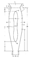
- In der einzigen Figur der Zeichnung ist in erheblich vergrößertem Maßstab der neuerungswesentliche Längenbereich eines Einpreßkontaktes, nämlich der mittlere Schaftteil desselben gezeigt, der zur einen Seite hin mit einer Kontaktfeder und einem Kontaktstift und zur anderen Seite hin mit einem Anschlußstift baueinheitlich gefertigt ist.
- In der Zeichnung ist von einem Einpreßkontakt 1 zum Einpressen in ein durchkontaktiertes Loch einer Leiterplatte im wesentlichen nur der mittlere Schaftteil 2 zu sehen, an den sich nach oben über eine Einpreßschulter 3 einstückig eine Kontaktfeder oder ein Kontaktstift 4 anschließt, die bzw. der nur andeutungsweise gezeigt ist.
- Unten ist, ebenfalls einstückig, mit dem Schaftteil 2 ein Anschlußstift 5 verbunden, von dem ebenfalls nur andeutungsweise ein Teilstück gezeigt wird.
- Die Einpreßschulter 3 dient dem Zweck, den Einpreßweg des Schaftteils 2 in ein durchkontaktiertes Loch 6 einer Leiterplatte 7 zu begrenzen, wobei die Oberseite der Leiterplatte 7 und das Loch 6 nur andeutungsweise - durch strichpunktierte Linien - gezeigt sind.
- Der Schaftteil 2 ist mit einer Schlitzöffnung 8 versehen, deren Enden 9 und 10 jeweils eine parabolische Ausbildung haben, während ihre Mitte eine Einschnürung 11 aufweist.
- Das der Kontaktfeder bzw. dem Kontaktstift 4 zugewendete Ende 9 der Schlitzöffnung reicht nahezu an die Einpreßschulter 3 heran, hat also nur einen geringen Abstand 12 zu dieser. Das andere Ende 10 der Schlitzöffnung 8 liegt hingegen in einem gewissen Abstand 13 von dem Übergang zwischen dem Schaftteil 2 und dem Anschlußstift 5. Erkennbar ist in der Zeichnung auch, daß der Schaftteil 2 sich von der Mitte seiner Länge bis zum Anschlußstift 5, also über den Längenbereich 14 hinweg von seiner maximalen Breite 15 auf ein Maß 16 verjüngt, welches etwa der Hälfte der maximalen Breite 15 entspricht.
- Zwischen den beiden Abständen 12 und 13 ist die Länge 17 der Schlitzöffnung 8 begrenzt. Beidseitig der Schlitzöffnung 8 weist der mittlere Schaftteil 2 des Einpreßkontaktes 1 je einen Schenkel 18 und 19 auf. Die Gesamtlänge 20 des mittleren Schaftteils 2 entspricht der Länge 17 der Schlitzöffnung 8 zuzüglich der beiden Abstände 12 und 13.
- Die Schlitzöffnung 8 hat im mittlerem Schaftteil 2 eine solche Lage, daß die dem Abstand 13 entsprechende Restlänge des Schaftteils 2 zu dem der halben Länge desselben entsprechenden Längenbereich 14 in einem Verhältnis steht, welches zwischen 0,45:1 und 0,35:1 liegt und dabei vorzugsweise etwa 0,4:1 beträgt.
- Es hat sich gezeigt, daß durch diese Gestaltung und Lage der Schlitzöffnung 8 die diese seitlich begrenzenden Schenkel 18 und 19 des mittleren Schaftteils 2 elastischer werden. Dies hat zur Folge, daß Einpreßkraft und Auspreßkraft für die Einpreßkontakte 1 annähernd gleich groß ausfallen und somit einen Indikator für eine gute Kontaktgabe zwischen dem mittleren Schaftteil 2 und dem durchkontaktierten Loch 6 in der Leiterplatte 7 liefern.
- Bei dem in der Zeichnung dargestellten Ausführungsbeispiel steht die dem Abstand 13 entsprechende Restlänge des Schaftteils 2 zur Länge 17 der Schlitzöffnung 8 in einem Verhältnis von bspw. 0,314:1 und der Abstand 12 zur Länge 17 der Schlitzöffnung 8 in einem Verhältnis von bspw. 0,12:1.
- Weiterhin ist der Einpreßkontakt 1 nach der Zeichnung so ausgeführt, daß die Länge 17 der Schlitzöffnung 8 zur Gesamtlänge 20 des mittleren Schaftteils 2 in einem Verhältnis von etwa 0,7:1 steht.
- Vorgesehen ist bei dem Einpreßkontakt nach der Zeichnung auch, daß die Breite der Schlitzöffnung 8 im Bereich der Einschnürung 11 zur größten Breite derselben im Bereich der parabolischen Enden 9 und 10 ein Verhältnis von etwa 0,73:1 bis 0,74:1 hat.
bei dem die Kontaktfeder oder der Kontaktstift im Übergangsbereich zum Schaftteil eine Einpreßschulter aufweist, die den Einpreßweg des Einpreßkontaktes begrenzt, und
bei dem der Schaftteil mit einer seitlich von Schenkeln begrenzten Schlitzöffnung versehen ist, wobei das der Kontaktfeder bzw. dem Kontaktstift zugewendete Ende der Schlitzöffnung nahezu an die Einpreßschulter heranreicht, während deren anderes Ende in einem gewissen Abstand vom Übergang zwischen dem Schaftteil und dem Anschlußstift liegt.
Claims (3)
- Einpreßkontakt zum Einpressen in ein durchkontaktiertes Loch einer Leiterplatte mit- einer Kontaktfeder oder einem Kontaktstift,- einem sich daran anschließenden mittleren Schaftteil und- einem eine Verlängerung des mittleren Schaftteils bildenden Anschlußstift,bei dem die Kontaktfeder oder der Kontaktstift im Übergangsbereich zum Schaftteil eine Einpreßschulter aufweist, die den Einpreßweg des Einpreßkontaktes in die Leiterplatte begrenzt und
bei dem der Schaftteil mit einer seitlich von Schenkeln begrenzten Schlitzöffnung versehen ist,
wobei das der Kontaktfeder bzw. dem Kontaktstift zugewendete Ende der Schlitzöffnung nahezu an die Einpreßschulter heranreicht, während deren anderes Ende in einem gewissen Abstand vom Übergang zwischen dem Schaftteil und dem Anschlußstift liegt,
dadurch gekennzeichnet,
daß die Schlitzöffnung an ihren Enden eine parabolische Ausbildung hat, während sie in ihrer Mitte durch Verbreiterung der Schenkel eine Einschnürung aufweist. - Einpreßkontakt nach Anspruch 1,
dadurch gekennzeichnet,
der Schaftteil sich von der Mitte seiner Länge bis zum Anschlußstift annähernd linear auf die Hälfte seiner maximalen Breite verjüngt,
und die Restlänge des Schaftteils zwischen dem Anschlußstift und dem diesem zugewendeten Ende der Schlitzöffnung einem Bruchteil der halben Länge des Schaftteiles entspricht. - Einpreßkontakt nach den Ansprüchen 1 und 2,
dadurch gekennzeichnet,
daß das Verhältnis der Restlänge (13) des Schaftteils (2) zur halben Länge (14) des Schaftteils (2) im Bereich zwischen 0,45:1 und 0,35:1, vorzugsweise etwa bei 0,4:1 liegt.
Applications Claiming Priority (2)
| Application Number | Priority Date | Filing Date | Title |
|---|---|---|---|
| DE9004090U DE9004090U1 (de) | 1990-04-09 | 1990-04-09 | Einpreßkontakt |
| DE9004090U | 1990-04-09 |
Publications (2)
| Publication Number | Publication Date |
|---|---|
| EP0451674A1 true EP0451674A1 (de) | 1991-10-16 |
| EP0451674B1 EP0451674B1 (de) | 1995-06-28 |
Family
ID=6852746
Family Applications (1)
| Application Number | Title | Priority Date | Filing Date |
|---|---|---|---|
| EP91105213A Expired - Lifetime EP0451674B1 (de) | 1990-04-09 | 1991-04-02 | Einpresskontakt |
Country Status (2)
| Country | Link |
|---|---|
| EP (1) | EP0451674B1 (de) |
| DE (2) | DE9004090U1 (de) |
Cited By (8)
| Publication number | Priority date | Publication date | Assignee | Title |
|---|---|---|---|---|
| US5823830A (en) * | 1995-02-24 | 1998-10-20 | Wurster; Woody | Tailess compliant contact |
| EP0887883A2 (de) * | 1997-06-24 | 1998-12-30 | ELCO Europe GmbH | Einpresskontakt |
| DE19831672B4 (de) * | 1998-07-15 | 2005-05-12 | Ludger Sorig | Einpreßkontakt |
| DE202016105003U1 (de) | 2016-09-09 | 2016-09-23 | Andreas Veigel | Steckverbinder |
| WO2020228974A1 (de) | 2019-05-15 | 2020-11-19 | Andreas Veigel | Drahtverbindungselement |
| DE202020105848U1 (de) | 2020-10-13 | 2022-02-10 | Andreas Veigel | Drahtverbindungselement |
| DE202020107455U1 (de) | 2020-12-22 | 2022-03-29 | Andreas Veigel | Leiterplattensteckverbinder |
| DE202022102403U1 (de) | 2022-05-03 | 2022-05-23 | Andreas Veigel | Steckverbinder |
Families Citing this family (4)
| Publication number | Priority date | Publication date | Assignee | Title |
|---|---|---|---|---|
| DE10229331B4 (de) * | 2002-06-29 | 2016-03-24 | Conti Temic Microelectronic Gmbh | Einpresskontakt |
| US7008272B2 (en) | 2003-10-23 | 2006-03-07 | Trw Automotive U.S. Llc | Electrical contact |
| DE202011004165U1 (de) | 2011-03-19 | 2011-07-20 | Elco Europe Gmbh | Einpresskontakt |
| FR2985864B1 (fr) * | 2012-01-12 | 2014-02-07 | Loupot | Contact pour emmanchement en force |
Citations (2)
| Publication number | Priority date | Publication date | Assignee | Title |
|---|---|---|---|---|
| EP0148792A2 (de) * | 1984-01-12 | 1985-07-17 | H & V SERVICES | Sich verformender Stift |
| EP0234235A1 (de) * | 1986-01-30 | 1987-09-02 | THE PLESSEY COMPANY plc | Kontaktstift |
Family Cites Families (1)
| Publication number | Priority date | Publication date | Assignee | Title |
|---|---|---|---|---|
| US4857018A (en) * | 1988-09-01 | 1989-08-15 | Amp Incorporated | Compliant pin having improved adaptability |
-
1990
- 1990-04-09 DE DE9004090U patent/DE9004090U1/de not_active Expired - Lifetime
-
1991
- 1991-04-02 EP EP91105213A patent/EP0451674B1/de not_active Expired - Lifetime
- 1991-04-02 DE DE59105821T patent/DE59105821D1/de not_active Expired - Fee Related
Patent Citations (2)
| Publication number | Priority date | Publication date | Assignee | Title |
|---|---|---|---|---|
| EP0148792A2 (de) * | 1984-01-12 | 1985-07-17 | H & V SERVICES | Sich verformender Stift |
| EP0234235A1 (de) * | 1986-01-30 | 1987-09-02 | THE PLESSEY COMPANY plc | Kontaktstift |
Cited By (15)
| Publication number | Priority date | Publication date | Assignee | Title |
|---|---|---|---|---|
| US5823830A (en) * | 1995-02-24 | 1998-10-20 | Wurster; Woody | Tailess compliant contact |
| EP0887883A2 (de) * | 1997-06-24 | 1998-12-30 | ELCO Europe GmbH | Einpresskontakt |
| EP0887883A3 (de) * | 1997-06-24 | 1999-12-08 | ELCO Europe GmbH | Einpresskontakt |
| DE19831672B4 (de) * | 1998-07-15 | 2005-05-12 | Ludger Sorig | Einpreßkontakt |
| DE202016105003U1 (de) | 2016-09-09 | 2016-09-23 | Andreas Veigel | Steckverbinder |
| DE102017119432A1 (de) | 2016-09-09 | 2018-03-15 | Andreas Veigel | Steckverbinder |
| WO2020228974A1 (de) | 2019-05-15 | 2020-11-19 | Andreas Veigel | Drahtverbindungselement |
| CN113557638A (zh) * | 2019-05-15 | 2021-10-26 | A·维格尔 | 线材连接元件 |
| US11831115B2 (en) | 2019-05-15 | 2023-11-28 | Andreas Veigel | Wire-connecting element |
| CN113557638B (zh) * | 2019-05-15 | 2024-02-02 | A·维格尔 | 线材连接元件 |
| DE202020105848U1 (de) | 2020-10-13 | 2022-02-10 | Andreas Veigel | Drahtverbindungselement |
| DE202020107455U1 (de) | 2020-12-22 | 2022-03-29 | Andreas Veigel | Leiterplattensteckverbinder |
| WO2022135839A1 (de) | 2020-12-22 | 2022-06-30 | Andreas Veigel | Leiterplattensteckverbinder |
| DE202022102403U1 (de) | 2022-05-03 | 2022-05-23 | Andreas Veigel | Steckverbinder |
| WO2023213469A1 (de) | 2022-05-03 | 2023-11-09 | Andreas Veigel | Leiterplatteneinpresskontakt |
Also Published As
| Publication number | Publication date |
|---|---|
| EP0451674B1 (de) | 1995-06-28 |
| DE59105821D1 (de) | 1995-08-03 |
| DE9004090U1 (de) | 1990-06-13 |
Similar Documents
| Publication | Publication Date | Title |
|---|---|---|
| EP0887883B1 (de) | Einpresskontakt | |
| DE69500024T2 (de) | Allgemein einsetzbare Auswurfvorrichtung für einen IC-Kartenverbinder | |
| DE69709987T2 (de) | Verbinder für Leiterplatte | |
| DE69204024T2 (de) | Elektrischer Flachbauverbinder. | |
| DE3241061C2 (de) | Elastischer Einpreßstift für die lötfreie Verbindung der Wickelpfosten elektrischer Steckverbinder o.dgl. mit durchkontaktierten Leiterplatten sowie Verfahren zu seiner Herstellung | |
| EP0160121B1 (de) | Elektromagnet für elektrische Schaltgeräte, insbesondere Schütze | |
| DE2435461C2 (de) | Elektrischer Kontaktstift | |
| EP0925617A1 (de) | Übergang von einem hohlleiter auf eine streifenleitung | |
| DE2406125A1 (de) | Buchsenkontakt | |
| DE2712833A1 (de) | Elektrische kontaktklemme | |
| EP0451674B1 (de) | Einpresskontakt | |
| DE102015102840A1 (de) | Klemmfederverbinder | |
| DE3828277C2 (de) | An einer Tragschiene anbringbare Schalteinheit mit zwei elektromagnetischen Kontakteinrichtungen | |
| DE2825201C2 (de) | Kontaktvorrichtung | |
| EP0432743B1 (de) | Wundklammer, insbesondere chirurgischer Mikroclip | |
| DE69919189T2 (de) | Spielzeugbausatz | |
| DE69015243T2 (de) | Anschlussvorrichtung. | |
| EP0226907A2 (de) | Relais | |
| CH678776A5 (en) | Supplementary terminal for large flat or round cables - clips cable under existing screw head with contact pressure maintained by leaf spring between two portions | |
| DE9310630U1 (de) | An einer Montagefläche befestigtes elektrisches Gerät | |
| DE3323861A1 (de) | Einstellvorrichtung fuer die vorspannkraft einer feder | |
| EP0980116A1 (de) | Sockelklemme, Sockel mit Klemme und Verfahren zur Herstellung der Klemme | |
| DE2816041C2 (de) | Stimmgabel und Verfahren zu deren Herstellung | |
| EP1360706A1 (de) | Federkappe und elektrisches bauelement | |
| DE2551970A1 (de) | Elektrische flachsteckbuchsen |
Legal Events
| Date | Code | Title | Description |
|---|---|---|---|
| PUAI | Public reference made under article 153(3) epc to a published international application that has entered the european phase |
Free format text: ORIGINAL CODE: 0009012 |
|
| 17P | Request for examination filed |
Effective date: 19910422 |
|
| AK | Designated contracting states |
Kind code of ref document: A1 Designated state(s): BE CH DE FR GB IT LI NL |
|
| RAP3 | Party data changed (applicant data changed or rights of an application transferred) |
Owner name: ELCO EUROPE GMBH |
|
| 17Q | First examination report despatched |
Effective date: 19940201 |
|
| GRAA | (expected) grant |
Free format text: ORIGINAL CODE: 0009210 |
|
| AK | Designated contracting states |
Kind code of ref document: B1 Designated state(s): BE CH DE FR GB IT LI NL |
|
| PG25 | Lapsed in a contracting state [announced via postgrant information from national office to epo] |
Ref country code: NL Free format text: LAPSE BECAUSE OF FAILURE TO SUBMIT A TRANSLATION OF THE DESCRIPTION OR TO PAY THE FEE WITHIN THE PRESCRIBED TIME-LIMIT Effective date: 19950628 Ref country code: GB Effective date: 19950628 |
|
| REF | Corresponds to: |
Ref document number: 59105821 Country of ref document: DE Date of ref document: 19950803 |
|
| ITF | It: translation for a ep patent filed | ||
| ET | Fr: translation filed | ||
| NLV1 | Nl: lapsed or annulled due to failure to fulfill the requirements of art. 29p and 29m of the patents act | ||
| GBV | Gb: ep patent (uk) treated as always having been void in accordance with gb section 77(7)/1977 [no translation filed] |
Effective date: 19950628 |
|
| REG | Reference to a national code |
Ref country code: CH Ref legal event code: NV Representative=s name: ULRICH UND BRIGITTE BALLMER PATENTANWAELTE |
|
| PLBE | No opposition filed within time limit |
Free format text: ORIGINAL CODE: 0009261 |
|
| STAA | Information on the status of an ep patent application or granted ep patent |
Free format text: STATUS: NO OPPOSITION FILED WITHIN TIME LIMIT |
|
| 26N | No opposition filed | ||
| PGFP | Annual fee paid to national office [announced via postgrant information from national office to epo] |
Ref country code: BE Payment date: 20080522 Year of fee payment: 18 Ref country code: IT Payment date: 20080426 Year of fee payment: 18 |
|
| PGFP | Annual fee paid to national office [announced via postgrant information from national office to epo] |
Ref country code: FR Payment date: 20090414 Year of fee payment: 19 Ref country code: DE Payment date: 20090422 Year of fee payment: 19 |
|
| PGFP | Annual fee paid to national office [announced via postgrant information from national office to epo] |
Ref country code: CH Payment date: 20090417 Year of fee payment: 19 |
|
| BERE | Be: lapsed |
Owner name: *ELCO EUROPE G.M.B.H. Effective date: 20090430 |
|
| PG25 | Lapsed in a contracting state [announced via postgrant information from national office to epo] |
Ref country code: BE Free format text: LAPSE BECAUSE OF NON-PAYMENT OF DUE FEES Effective date: 20090430 |
|
| REG | Reference to a national code |
Ref country code: CH Ref legal event code: PL |
|
| REG | Reference to a national code |
Ref country code: FR Ref legal event code: ST Effective date: 20101230 |
|
| PG25 | Lapsed in a contracting state [announced via postgrant information from national office to epo] |
Ref country code: LI Free format text: LAPSE BECAUSE OF NON-PAYMENT OF DUE FEES Effective date: 20100430 Ref country code: DE Free format text: LAPSE BECAUSE OF NON-PAYMENT OF DUE FEES Effective date: 20101103 Ref country code: CH Free format text: LAPSE BECAUSE OF NON-PAYMENT OF DUE FEES Effective date: 20100430 |
|
| PG25 | Lapsed in a contracting state [announced via postgrant information from national office to epo] |
Ref country code: IT Free format text: LAPSE BECAUSE OF NON-PAYMENT OF DUE FEES Effective date: 20090402 |
|
| PG25 | Lapsed in a contracting state [announced via postgrant information from national office to epo] |
Ref country code: FR Free format text: LAPSE BECAUSE OF NON-PAYMENT OF DUE FEES Effective date: 20100430 |