EP0448727B1 - Plasmaanzeigetafel und herstellungsverfahren derselben - Google Patents
Plasmaanzeigetafel und herstellungsverfahren derselben Download PDFInfo
- Publication number
- EP0448727B1 EP0448727B1 EP90915195A EP90915195A EP0448727B1 EP 0448727 B1 EP0448727 B1 EP 0448727B1 EP 90915195 A EP90915195 A EP 90915195A EP 90915195 A EP90915195 A EP 90915195A EP 0448727 B1 EP0448727 B1 EP 0448727B1
- Authority
- EP
- European Patent Office
- Prior art keywords
- diaphragm
- electrodes
- group
- glass
- plasma display
- Prior art date
- Legal status (The legal status is an assumption and is not a legal conclusion. Google has not performed a legal analysis and makes no representation as to the accuracy of the status listed.)
- Expired - Lifetime
Links
Images


Classifications
-
- H—ELECTRICITY
- H01—ELECTRIC ELEMENTS
- H01J—ELECTRIC DISCHARGE TUBES OR DISCHARGE LAMPS
- H01J17/00—Gas-filled discharge tubes with solid cathode
- H01J17/02—Details
- H01J17/16—Vessels; Containers
-
- H—ELECTRICITY
- H01—ELECTRIC ELEMENTS
- H01J—ELECTRIC DISCHARGE TUBES OR DISCHARGE LAMPS
- H01J17/00—Gas-filled discharge tubes with solid cathode
- H01J17/38—Cold-cathode tubes
- H01J17/48—Cold-cathode tubes with more than one cathode or anode, e.g. sequence-discharge tube, counting tube, dekatron
- H01J17/49—Display panels, e.g. with crossed electrodes, e.g. making use of direct current
Definitions
- the present invention relates to a plasma display panel having a first group of parallel electrodes and a second group of parallel electrodes and comprising a front glass plate, a back plate and a diaphragm therebetween, said front glass plate and said back plate being sealed together, said diaphragm having an upper surface and a lower surface and consisting of a metallic sheet having a plurality of apertures for permitting discharge, said aperture being filled with an ionizable gas.
- the invention further relates to a method of producing a plasma display panel as defined in the preambles of claims 8 and 9.
- PDPs plasma display panels
- the periphery thereof is sealed with glass to constitute a housing and the gap is filled with a gas so that the panel is flat.
- the front plate must be composed of a glass plate and the other back plate is also composed of a glass plate of the same kind since it is inexpensive. Therefore, the following description deals with the PDP of this type.
- the air is exhausted prior to filling with a gas causing the pressure differential to become the greatest between the inside and the outside of the housing. Due to this pressure differential, the two pieces of glass substrates undergo a deformation. The deformation further increases due to the heating that is effected to release the gas that is adsorbed in the housing. In order to suppress the deformation to a negligible degree, the thickness of the glass plates must be increased or the size of the panel must be decreased. Such a limitation can be removed if spacers are provided between the two pieces of glass plates; i.e., spacers are indispensable for large display panels.
- diaphragms or spacers are usually necessary to maintain a suitable gap for electric discharge or to prevent crosstalk relative to the neighbouring cells irrespective of the type of electric discharge such as the AC type or the DC type.
- the arrangement of discharge cells in the PDP is determined depending upon the object of its use, and examples include a figure-eight display consisting of seven segments, a character display consisting of 5 x 7 dots, a full-dot display consisting of 640 x 480 dots, and the like.
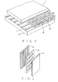
- Figs. 1 to 5 illustrate arrangements of discharge cells in the PDPs, and wherein reference numeral 1 denotes a front glass plate, 3 denotes a diaphragm, 5 denotes a back glass plate, 6 denotes positive electrodes, and reference numeral 7 denotes negative electrodes.
- diaphragms and spacers hereinafter often referred to simply as diaphragms
- the diaphragm can be prepared by the same method for any arrangement of cells, and a variety of methods have heretofore been attempted such as:
- the method A is excellent in regard to economy and mass-produceability but has a defect in that a gap large enough for electric discharge is not obtained unless the printing is repeated many times.
- making the dot pitch very fine e.g., 0.2mm of dot pitch
- a fine dot pitch was accomplished in the shape of stripes as shown in Fig. 2 (Y. Amano: SID Int. Symp. dig. Tech. Paper, p. 160, 1982), which, however, cannot be applied to diaphragms that completely surround the discharge cells as shown in Figs. 1 and 4, and is not practical since it requires a very high degree of technology.
- a luminous colour of a rare gas itself such as a PDP of an orange luminous colour by the electric discharge of a neon gas
- even the incompletely closed diaphragm can be put into practical use since the emission of light is limitied to the proximity of electrodes of the selected cell.
- the electric discharge tends to take place among the neighbouring cells.
- the light is emitted by exciting the fluorescent material using ultraviolet rays produced by the electric discharge.
- the ultraviolet rays leak causing the fluorescent material of the neighbouring cells to be excited and resulting in the emission of light. That is, the crosstalk or the colour blurring develops inevitably to impair the colour reproduceability and resolution, and the display panel loses its value.
- the method A is not suited for preparing a highly fine and completely closed diaphragm, and is not practical for realizing the colour PDP.
- the method B makes it relatively easy to accomplish the display panel maintaining high accuracy using, however, a very special photosensitive glass having this disadvantage of cost and economy. Moreover, fabricating a glass sheet which is as thin as 0.1 to 0.5mm is not practical since the glass becomes brittle.
- the present invention was achieved in view of the above-mentioned problems inherent in the prior art, and its object is to provide a PDP which satisfies the demand for high accuracy and which is excellent in economy and mass-produceability.
- the invention further supplies a method of producing a plasma display panel as defined in claims 8 and 9.
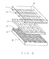
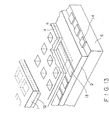
- Fig. 6 is a diagram showing parts for constituting the PDP of the DC type according to an embodiment of the present invention under the condition where the parts are being assembled.
- positive electrodes 6 are provided on a front glass plate 1 and negative electrodes 7 are provided on a back glass plate 5. Furthermore, a lattice type diaphragm 4 consisting of a metal plate with apertures for discharge is arranged between the front glass plate 1 and the back glass plate 5, and insulating layers 2 are positioned between the front glass plate 1, the back glass plate 5 and the lattice type diaphragm 4 in order to electrically insulate the diaphragm 4 with apertures of the lattice type from the positive electrodes 6 and the negative electrodes 7.
- Fig. 7 shows parts for constituting the PDP of the DC type according to another embodiment of the present invention under the condition where the parts are being assembled
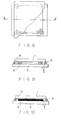
- Fig. 8 is a plan view after the parts are assembled
- Fig. 9 is a vertical section view of when a cellular space is cut along the A-A' cross section of Fig. 8
- Fig. 10 is a vertical section view of the case when the diaphragm is cut along the A-A' cross section of Fig. 8.
- reference numerals denote the same portions as those of Fig. 6.
- the lattice type diaphragm 4 consisting of the metal has a dielectric layer that is deposited thereon to form an insulating layer.
- Reference numeral 8 denotes spacers
- 9 denotes a sealing glass.
- the metal plate that serves as a diaphragm or a spacer is composed of an alloy that contains at least one kind of element selected from iron, cobalt, nickel or chromium, and should preferably have a coefficient of linear thermal expansion of 40 to 100 x 10 -7 /°C (at 25° to 500°C).
- the metal plate that is used has a thickness of 0.01 to 1.0 mm, and preferably 0.05 to 0.1 mm.
- the periphery of the diaphragm or the space that is sandwiched by two sheets of glass plates is sealed with glass to place a gas therein. Therefore, the diaphragm (spacer), two sheets of glass plates, and the sealing glass must have coefficients of linear thermal expansion which are nearly equal or close to each other. Otherwise, the glass may be broken due to an excess stress when cooled after the sealing.
- the metal plate should desirably have a coefficient of linear thermal expansion of 80 to 100 x 10 -7 /°C (at 25° to 500°C).
- the metal materials that are suitable may include a 42wt%Ni - 6wt%Cr - Fe alloy, 50wt%Ni - Fe alloy, and the like alloys.
- the metal plate should desirably have a coefficient of linear thermal expansion of 40 to 60 x 10 -7 /°C (at 25° to 500°C) to meet therewith.
- An example of the metal material that is suitable may be a 20wt%Ni - 17wt%Co - Fe alloy.
- the material of the diaphragm should be selected accordingly.
- the metal material composition consideration is given to the price, workability and mechanical properties in addition to the coefficient of linear thermal expansion.
- the heat resistance in the step of sealing is usually carried out at 400° to 500°C, and the alloys mentioned above are sufficiently usable at this temperature.
- the step of sealing can be simply carried out in an open atmosphere. In this case, though the resistance of the metal material against the oxidation becomes a problem, the above-mentioned alloys are sufficiently usable. Even when there remains a problem in regard to the resistance against the oxidation, the metal material can be used by making the sealing atmosphere nonoxidizing or by forming an oxidation-resistant film by the well-known metal surface treatment.
- a predetermined pattern with apertures for discharge is formed in the metal plate by, for example, punching using a press, laser machining, plating method, welding method, etching method or a like method. There should be used the most advantageous method by taking the machining distortion, machining precision and machining cost into consideration. Generally, however, the etching method is preferred.
- the apertures in the metal plate may be made in any shape and arrangement, such as in a lattice type, stripe type, circular type, delta arrangement or seven-segment type as shown in Figs. 1 to 5. According to the present invention, however, the highly fine and completely closed diaphragms are preferred as shown in Figs. 1 and 4 and, in particular, the lattice type shown in Fig. 1 is preferred.
- the numerical aperture of the display cells becomes a problem since ineffective display portion increases due to the diaphragm.
- the highly fine panel usually uses the diaphragm having a height of 100 to 200 ⁇ m. In this range, there can be utilized the aforementioned realistic diaphragm-forming method, i.e., the thick-film printing method.
- the height is smaller than 100 ⁇ m, the effect of cathode sputtering becomes too great in the case of the DC type, and it further becomes difficult to uniformalize the discharge characteristics over a number of cells.
- the printing must be carried out an increased number of times resulting in an increase in the cost.
- the minimum width of the diaphragm that can be formed by the thick-film printing method is about 80 ⁇ m in the case of the stripe type and about 150 ⁇ m in the case of the lattice type.
- a minimum diaphragm width of about 20 ⁇ m is accomplished when the thickness is about 50 ⁇ m and a minimum diaphragm width of about 30 ⁇ m is accomplished when the thickness is about 100 ⁇ m by the etching method.
- the numerical aperture becomes about 56% in the case of the thick-film printing method and about 90% in the case of a piece of metal plate, creating a difference of about 1.6 times in numerical aperture. This difference further increases with a decrease in the dot pitch.
- the diaphragm having a further increased numerical aperture can be formed if thin metal plates are used in combination.
- the present invention makes use of the metal plate with apertures that is formed in a desired shape as a diaphragm.
- the discharge electrodes have been arranged on the front plate and/or the back plate, and there will be no problem when the electrodes are covered by a dielectric member as in the PDP of the AC type.
- the metal plate (diaphragm) that is sandwiched and sealed between the front plate and the back plate comes in electric contact with the electrodes.
- the insulating layer may be formed on the electrodes on the front plate and on the back plate.
- An insulating layer is provided on at least one of the surfaces of the metal plate (diaphragm).
- the insulating layer is deposited by a variety of technologies such as spray method, printing method, electrostatic coating method, dipping method, anodic oxidation method, heat oxidation method, sputtering method, melt-injection method and electrodeposition method, and any one of them can be selected by taking the cost, performance and the like into consideration. The following two methods are preferred.
- the first method is the electrodeposition method by which nearly the entire surface of the porous metal plate is coated with a dielectric material to form an insulating layer.
- the electrodeposition method is achieved by using the metal plate as an electrode, by dispersing a glass and a dielectric powder including the glass in a solution that contains an electrolyte, and by applying an electric field thereto.
- the particle size should desirably be form 0.1 to 5 ⁇ m though it may differ depending upon the insulating layer that is required.
- the dispersion solution may be an isopropyl alcohol and the electrolyte may be Al 2 (NO 3 ) 3 , Ba(NO 3 ) 2 , which, however, can be selected from many widely known ones.
- the powder that is electrodeposited is heated to melt the glass, whereby the insulating layer is intimately adhered nearly on the entire surface of the porous metal plate.
- the insulating layer that is too thick is not desirable from the standpoint of reducing the space of the discharge cell.
- the insulating layer should have a thickness of from 1 to 10 ⁇ m.
- the metal plate that is provided with the insulating layer over nearly the entire surface maintains electric insulation relative to the discharge electrodes and further offers the following advantage. If the diaphragm is constituted by the dielectric material alone, the electrically conductive material that is sputtered by the electric discharge is deposited on the dielectric material in such small amounts that there arises no problem of short-circuiting among the electrodes.
- the metal plate is used as a diaphragm as in the present invention and if the distance of insulation is short between the electrodes and the porous metal plate.
- the diaphragm can be constituted in the same manner as the conventional one which is made of a dielectric eliminating the probability of short-circuiting.
- the second method consists of transferring the insulating layer onto the surface of the metal plate by utilizing the pressure or both the heat and the pressure.
- This method has been widely known and a variety of materials can be used therein as described below.
- the substrate that can be peeled off is composed of a polyester film on which a silicone film is formed, and a pressure-sensitive ink or a heat- and pressure-sensitive ink is composed of kneading a vehicle obtained by dissolving an acrylic resin in a solvent such as butylcarbitol acetate together with glass and a dielectric powder that contains the glass.
- the particle size should range from 0.1 to 5 ⁇ m.
- the ink is screenprinted on the substrate that can be peeled off to form an insulating layer which is then dried.
- the metal plate is placed on the film, the pressure is exerted upon them at ordinary temperature or under a heated condition, the insulating layer is adhered as a surface pattern onto the metal plate, and the substrate is peeled off thereby to transfer the insulating layer.
- the insulating layer is transferred onto one surface or both surfaces of the porous metal plate.
- the insulating layer that is transferred is then heated to melt the glass and is thus firmly adhered to the metal plate. If the firm adhesion is effected with the panel being in contact with the glass substrate, then the diaphragm can, at the same time, be firmly adhered onto the glass substrate.
- the above-mentioned transfer method gives a great advantage for the highly fine panels and, particularly, for those panels having small diaphragm width.
- the insulating layer is provided even on the side surfaces of the diaphragm as in the first method, it is allowed to reduce the area of the discharge cell even if the insulating layer has a reduced thickness.
- the insulating layer is provided on the surface only of the metal plate, it becomes difficult to print a highly fine pattern, the size tends to be easily deviated, and the ink spreads onto the side surfaces of the diaphragm due to blurring of ink, provided the screen-printing method or a like method is used instead of the transfer method.
- the difficulty can be understood if a highly fine panel is presumed having a diaphragm width of smaller than 100 ⁇ m and a cell pitch of smaller than 200 ⁇ m.
- the discharge panel operates sufficiently if the vicinity only of the discharge electrodes is insulated despite there exist electrically conductive portions. It was found through experiments that there exists no problem if the distance of insulation between the electrodes and the diaphragm metal is several ⁇ m or is about 10 ⁇ m just to maintain safety. Therefore, the insulating layer should have a thickness so as to obtain such a distance.
- the insulating layer (dielectric layer) formed on the metal plate has a thickness of 1 to 100 ⁇ m.
- the grooves for diffusing the gases can be reliably formed by any one of the following methods or by a combination of the following methods.
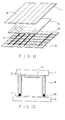
- Fig. 11 shows the parts constituting the PDP of the DC type under the condition where the parts are being assembled using the stripe type dielectric as in the aforementioned second method
- Fig. 12 is a section view showing the structure of a cell of the PDP.
- reference numerals denote the same members as those of Fig. 6.
- a dielectric layer is deposited on the lattice type diaphragm 4 which consists of a metal plate to form an insulating layer just like in Fig. 7.
- Reference numeral 10 denotes a stripe type dielectric
- 11 denotes a fluorescent material.
- the dielectric material used for the insulating layer consists of one or more of those selected from an organic material, crystalline inorganic material and glass. Generally, furthermore, a glass or a crystalline inorganic material containing the glass is used.
- the glass composition examples include PbO-B 2 O 3 -SiO 2 , PbO-B 2 O 3 , ZnO-B 2 O 3 -SiO 2 , and the like. These glasses should have softening points of 350° to 1000°C and glass particle sizes of about 1 to 5 ⁇ m.
- the glass used here is heated at a temperature (sealing temperature) at which the sealing glass frit is softened and melted in the step of sealing the PDP, but should not be melted again at this temperature.
- the sealing temperature of the glass frit is higher by about 50°C than the softening point thereof.
- the sealing temperature of the PDP should be about 400° to 450°C and, hence, the glass contained in the dielectric should have softening point which is higher than 350°C.
- the upper limit of the softening point is so determined that the metal will not undergo deformation and that the metal and the dielectric will not undergo the chemical reaction in large amounts, and should desirably be lower than 1000°C.
- examples of the crystalline inorganic material include ceramics such as alumina (Al 2 O 3 ), forsterite (2MgO-SiO 2 ) and the like, as well as inorganic pigments (FeO-Cr 2 O 3 , CoO-Al 2 O 3 , etc.).
- the crystalline inorganic materials should have particle sizes of about 1 to 5 ⁇ m.
- any organic material can be used provided it can finally turned into an inorganic material.
- the insulating layer In a general panel-sealing method (sealed with a sealing glass), the insulating layer must withstand the sealing temperature and must have a coefficient of linear thermal expansion which is nearly the same as those of the two pieces of glass plates, sealing glass and diaphragm. From such points of view, the above-mentioned materials are suitably selected.
- the metal plate that has electric conductivity can be used as an electrode.
- This electrode is electrically coupled among a number of cells and is not advantageous for being used as an electrode for selecting the display cells.
- auxiliary electric discharge Japanese Patent Laid-Open Gazette No. 115060/1979, Japanese Patent Laid-Open Gazette No. 30038/1983, journal of the Television Society, Vol. 40, No. 10, 1986, p. 953. Developing the auxiliary discharge over the whole cells simultaneously is effective, and the above porous metal plate can be used as the electrode for the auxiliary discharge.
- Fig. 13 shows parts for constituting the PDP in the condition where the parts are being assembled using the metal plate as the auxiliary discharge electrode
- Fig. 14 is a section view of the cells along the direction of the positive electrode.
- reference numerals denote the same portions as those of Fig. 6.
- a dielectric layer is deposited on the lattice type diaphragm 4 which consists of a metal thereby to form an insulating layer just like in Fig. 7.
- reference numeral 12 denotes a third electrode (positive electrode)
- 13 denotes a group of second electrodes (negative electrodes)
- 14 denotes first electrodes (trigger electrodes).
- a plurality of metal plates to form space for auxiliary discharge as shown in Figs. 13 and 14.
- the display is not interrupted by the auxiliary discharge electrode.
- the same method as the one for forming the aforementioned insulating layer can be employed here if it is necessary to provide an insulation among the plurality of metal plates.
- the auxiliary discharge electrode can be used even under the condition where the metal is exposed as is widely known or where it is covered by a dielectric layer.
- the positions are suitably designed to meet the electrode structure and shape of the panel.
- Use of the plurality of metal plates makes it possible to increase the degree of freedom for designing the distance among the electrodes that are opposed to each other, as well as to use thin metal plates provided the diaphragm has the same height. It is therefore allowed to form more fine cell pitches than when a piece of the porous metal plate is used. Or, if the cell pitch is the same, then there can be used the diaphragm having a small width, i.e., having a large numerical aperture.
- ultraviolet rays are usually generated by the electric discharge to excite a fluorescent material and to emit light.
- the fluorescent material is usually deposited on the front glass plate or on the back glass plate.
- the brightness of the emitted light increases with an increase in the area of the fluorescent material that is deposited. It is therefore desired to deposit the fluorescent material even on the side surfaces of the diaphragm, i.e., even on the inner surfaces of the apertures of the metal plates.
- the fluorescent material is usually in a powdery form from which a thick-film ink can be prepared.
- the fluorescent material is printed onto the portions using the ink.
- the ink often fails to reach the innermost part of the holes or clogs the holes if it reaches the innermost part.
- the fluorescent material is applied to the inner surfaces of the apertures maintaining a thickness depending upon the viscosity of the ink, and an excess of the ink is drained out of the holes.
- This method makes it possible to separately apply fluorescent materials of many colors even onto the inner surfaces of holes of the metal plate that has a cell pitch of smaller than 0.3 mm.
- the diaphragm of the present invention is realized in the completely closed type and offers a larger fluorescent material-deposited area than that of the incompletely closed diaphragm.
- the present invention uses a diaphragm made of a metal plate that is different from the customarily used dielectric (glass or inorganic material containing glass) diaphragm. Therefore, the cell shape, size and pitch of arrangement are greatly dependent upon the working precision of the thin metal plate, and sufficient precision is offered for forming dot sizes and dot pitches required by the PDPs of the AC type and the DC type that give ordinary dot matrix display. Moreover, the insulating layers electrically insulate the metal plate from the electrodes on the front plate and on the back plate.
- the PDP of the present invention that uses a metal plate as the diaphragm and that has an insulating layer, is capable of realizing a highly fine cell pitch maintaining excellent crosstalk characteristics. Moreover, no electric short-circuiting takes place among the positive electrodes - negative electrodes.
- a 42wt%Ni - 6wt%Cr - Fe alloy having a coefficient of linear thermal expansion of 92 x 10 -7 /°C was used as a metal material composition for the metal plate that serves as a diaphragm.
- the metal plate possessed a thickness of 0.1 mm, the arrangement of perforation was of the lattice form with many square apertures arranged in the vertical and lateral directions maintaining an equal pitch of 0.2 mm, the size of the apertures being 0.15 x 0.15 mm, and the apertures being obtained by etching to obtain the metal plate with apertures.
- the PDP was equipped with a transparent and electrically conductive film (ITO) that serves as positive electrode on the front glass plate and nickel that serves as negative electrodes on the back glass plate. Furthermore, a dielectric layer in the form of stripes was formed by screen-printing on the electrodes of the front glass plate and the back glass plate avoiding the display cell regions, thereby to form an insulating layer.
- ITO transparent and electrically conductive film
- the diaphragm of the DC-type PDP described in Example 1 was formed by the thick film-printing method.
- the diaphragm was prepared having a dot pitch of 1,0 mm and apertures measuring 0.8 x 0.8 mm.
- the diaphragm having a height of 0.15 mm was formed by repeating the printing eight times.
- the diaphragm of the DC-type PDP described in Example 1 was prepared by etching a photosensitive sheet glass. As mentioned earlier, however, this material is very expensive. Moreover, the sheet glass was so thin that it was very brittle and was inferior to that of the Example 1 even from the standpoint of assembling and workability.
- the diaphragm of the DC-type PDP like that of Comparative Example 2 was prepared by perforating a general soda lime glass or a like glass. When a number of apertures were made by this method maintaining a pitch as highly fine as about 0.2 mm, however, the dimensional accuracy was considerably lower than that of Comparative Example 2. Considering from the brittleness of the thin sheet glass, furthermore, the diaphragm was inferior to that of Comparative Example 2 from the standpoint of workability and assembling, and was hence considerably inferior to that of Example 1.
- the metal plate was used alone as a diaphragm without providing the insulating layer on the front glass plate and on the back glass plate. As a result, electrical short-circuiting took place among the positive electrodes - negative electrodes, the display panel did not turn on and often short-circuiting took place among the positive electrodes or among the negative electrodes causing the non-selected cells to emit light. Thus, the metal plate did not work as a diaphragm for the PDP.
- a dielectric was deposited on the lattice type metal plate that was used in Example 1 to form an insulating layer thereon.
- dielectric material As a dielectric material, use was made of an inorganic filler such as a ZnO-B 2 O 3 -SiO 2 type glass powder, Al 2 O 3 , FeO ⁇ Cr 2 O 3 or the like having a softening point of 600°C and an average particle size of 2 to 3 ⁇ m.
- the dielectric was electrodeposited in an electrodepositing solution using the lattice type metal plate as a negative electrode and using a metal plate made of the same material and having nearly the same area as a positive electrode being impressed with a voltage of DC 200 volts.
- the electrodeposited condition was very good and the electrodeposited layer exhibited very good strength.
- the above sample was fired at a temperature higher than 600°C which is the softening point of the glass powder to obtain a densely formed dielectric layer.
- a desired lattice type metal plate on which the surfaces were deposited the dielectric was obtained.
- the DC-type PDP was prepared as described below using, as a diaphragm, the lattice type metal plate on which the surface has been deposited the dielectric.
- the lattice type metal plate whose surfaces have been covered with the dielectric was used as a diaphragm 4, and a glass which is thicker than the diaphragm 4 by about 30 ⁇ m was used as the spacer 8.
- the diaphragm 4 and the spacer 8 were sandwiched between the front glass plate 1 and the back glass plate 5, and the periphery thereof was sealed with a glass 9 to form an X-Y matrix PDP of the DC type.
- the DC-type PDP was sealed well and there developed no problem such as breakage due to stress and strain.
- the spacer was located outside the display region of the PDP, a gas introduction space of about 30 ⁇ m always existed in the display region over the diaphragm, and the air could be exhausted and a gas could be filled reliably over the whole display region.
- the DC-type PDP was prepared as described below by using the lattice type metal plate on which the surface has been deposited the dielectric that was used in Example 2 and a stripe type dielectric.
- the stripe type dielectric was obtained by forming a dielectric layer having a line width of 50 ⁇ m on the back glass plate maintaining a thickness of 30 ⁇ m and a pitch of 0.2 mm.
- the lattice type metal plate 4 on which has been deposited the dielectric and the stripe type dielectric 10 were sandwiched between the front glass plate 1 and the back glass plate 5 so as to use them as a diaphragm, followed by the sealing with a low-melting glass frit. Then, the air therein was evacuated and a gas was placed therein through a chip tube which was then sealed and chipped off to prepare a PDP of the DC type.
- positive electrodes 6 are provided on the front glass plate 1 and a fluorescent material 11 is applied onto the inner surface of the front glass plate 1. Further, the back glass plate 5 is provided with negative electrodes 7.
- the positive electrodes 6 and the negative electrodes 7 meet at right angles to form a dot matrix.
- the DC-type PDP having a dot number of 100 x 100.
- the gas having a composition He-Xe(2%) was filled under 300 Torr.
- the thus obtained DC type PDP was excellent with respect to adaptability toward enhancing the accuracy, workability, uniformity in the discharge voltage characteristics, and crosstalk characteristics.
- the PDP of the DC type was prepared as described below using as a diaphragm the metal plate with apertures of the lattice type on which the surface has been deposited the dielectric that was used in Example 2.
- a thin aluminum film was formed into stripes maintaining a pitch of 0.2 mm a dielectric layer 2 was formed thereon by kneading a vehicle together with a powder consisting of a ZnO-B 2 O 3 -SiO 2 type glass powder and a small amount of Al 2 O 3 to obtain a paste thereof, solid-printing the paste by the screen-printing method and firing it at 580°C.
- second electrodes 13 were formed in a shape of stripes on the dielectric layer in a direction to meet the first electrodes 14 at right angles, based on the screen printing method using a nickel paste maintaining a pitch of 0.2 mm and a line width of 0.1 mm and firing it at 580°C.
- the metal plate that serves as a third electrode 12 was made of a metal plate having the same material and the same shape as the substrate metal consisting of the metal plate that served as the diaphragm 4.
- the diaphragm 4 consists of two pieces of metal plates.
- the diaphragm 4 consisting of the thus obtained metal plates was placed on the back glass plate 5, sandwiched by the front glass plate 1 that has the third electrode 12, followed by the sealing with a low-melting glass frit. Then, the air therein was evacuated and a gas was filled through a chip tube which was then cut off to obtain a PDP of the DC type.
- the gas having a composition Ne-Ar(0.5%) was filled under 350 Torr.
- the thus obtained DC-type PDP was excellent with respect to sputter resistance of the negative electrodes, current density of the negative electrodes, discharge-maintaining voltage and workability (mass-produceability).
- a 42wt%Ni - 6wt%Cr - Fe alloy having a coefficient of linear thermal expansion of 92 x 10 -7 /°C was used as the metal plate that served as the diaphragm.
- the metal plate possessed a thickness of 75 ⁇ m, the arrangement ofof perforation was of the lattice form with many square apertures arranged in the vertical and lateral directions maintaining an equal pitch of 0.2 mm, the size of the holes being 0.17 x 0.17 mm, and the number of apertures being perforated by etching to to obtain a metal plate (type A).
- another similar metal plate was prepared having a thickness of 75 ⁇ m, a cell pitch of 0.15 mm, and a hole size of 0.12 x 0.12 mm (type B).
- an inorganic filler such as a ZnO - B 2 O 3 - SiO 2 type glass powder, Al 2 O 3 , Fe 2 O 3 ⁇ Cr 2 O 3 or the like having a softening point of 800°C and an average particle size of 2 to 3 ⁇ m.
- An acrylic resin having adhesiveness under the application of heat and pressure was dissolved in an organic solvent such as BCA (butylcarbitol acetate) or pine oil to obtain a vehicle for transfer printing.
- the vehicle consisted of 5 to 20 parts by weight of a resin component and 80 to 95 parts by weight of a solvent component.
- the glass powder and the inorganic filler were kneaded in an amount of 60 to 80 parts by weight together with 20 to 40 parts by weight of the vehicle to obtain a paste for transfer printing.
- the paste was solid-printed by the screen-printing method on a polyester film that is a substrate that will be peeled off, and was dried to a sufficient degree at 90°C.
- the transfer sheet that was dried was press-adhered onto the metal plate using a hot roller or a hot flat press.
- the transfer sheet was peeled off, the metal plate on which the dielectric layer has been formed was fired in the open air at 600° to 680°C such that the dielectric layer became completely inorganic and dense, thereby to obtain an insulating layer on the surface of the metal plate.
- the PDP of the DC type was prepared as described below using the above metal plate as the diaphragm. That is, as shown in Fig. 6, the metal plate was used as the diaphragm 4 which was then sandwiched between the front glass plate 1 and the back glass plate 5 on which the electrodes have been formed, and the periphery thereof was sealed with a glass in order to form an X-Y matrix PDP of the DC type.
- the DC type PDP was sealed well and there developed no problem such as breakage due to stress and strain.
- the DC type PDP exhibited good results without decreasing the numerical aperture irrespective of either the type A or the type B having dissimilar cell pitch was used.
Claims (9)
- Plasmabildschirm mit einer ersten Gruppe paralleler Elektroden (6, 14) und einer zweiten Gruppe paralleler Elektroden (7,13), die eine Frontglasscheibe (1), eine Rückscheibe (5) und ein zwischen diesen beiden gelegenes Diaphragma (3, 4) aufweist, welche besagte Frontglasscheibe (1) und besagte Rückscheibe (5) aneinander geheftet sind und welches Diaphragma eine obere Oberfläche und eine untere Oberfläche hat, die aus einer Metallplatte mit einer Vielzahl an Öffnungen zur Weitergabe von Entladungen aufweist, welche Öffnungen mit ionisierbarem Gas verfüllt sind, dadurch gekennzeichnet, daß die Elektroden (6, 14) der ersten Gruppe und die Elektroden (7, 13) der zweiten Gruppe sich in parallelen Ebenen befinden, die einen bestimmten Abstand aufweisen, und in der senkrechten Sicht auf den Plasmabildschirm sich die Elektroden der ersten und der zweiten Gruppe kreuzen, das Diaphragma (3, 4) eine Dicke von 0,01 bis 1,0 mm hat, wenigstens eine der besagten oberen und unteren Oberflächen des besagten Diaphragmas (3, 4) mit einer dielektrischen Schicht (2) versehen ist, die aus einem dielektrischen Material in Glas besteht und der minimale Achsabstand der Reihe besagter Öffnungen kleiner als 0,6 mm ist.
- Plasmabildschirm mit einer ersten Gruppe paralleler Elektroden (6, 14) und einer zweiten Gruppe paralleler Elektroden (7, 13), die eine Frontglasscheibe (1), eine Rückscheibe (5) und ein zwischen diesen beiden gelegenes Diaphragma (3, 4) hat, welche besagte Frontglasscheibe (1) und besagte Rückscheibe (5) aneinander geheftet sind und welches Diaphragma eine obere Oberfläche und eine untere Oberfläche hat, die aus einer Metallplatte mit einer Vielzahl an Öffnungen zur Weitergabe von Entladungen aufweist, welche Öffnungen mit ionisierbarem Gas verfüllt sind, dadurch gekennzeichnet, daß sich die Elektroden (6, 14) der ersten Gruppe und die Elektroden (7, 13) der zweiten Gruppe in parallelen Ebene befinden, die einen bestimmten Abstand haben, und in der senkrechten Sicht auf den Plasmabildschirm sich die Elektroden der ersten und der zweiten Gruppe kreuzen, wenigstens eine der besagten oberen und unteren Oberflächen des besagten Diaphragmas (3, 4) mit einer dielektrischen Schicht (2) versehen ist, die aus einem dielektrischen Material in Glas besteht, welches Diaphragma (3, 4) als eine Entladungselektrode verwendet wird, die der besagten ersten und zweiten Gruppe von parallelen Elektroden hinzugefügt ist.
- Plasmabildschirm nach Anspruch 1 oder 2, dadurch gekennzeichnet, daß die besagte Metallplatte wenigstens ein Metall aufweist, das aus der Gruppe Eisen, Nickel, Chrom und Kobalt ausgewählt wird und einen linearen Expansionskoeffizienten von 40 x 10-7 / °C bis 100 x 10-7 / °C bei 25 bis 500 °C hat.
- Plasmabildschirm nach Anspruch 1 oder 2, dadurch gekennzeichnet, daß das Glas in der besagten dielektrischen Schicht (2) einen Erweichungspunkt von 350 bis 1000 °C hat.
- Plasmabildschirm nach Anspruch 1 oder 2, dadurch gekennzeichnet, daß die dielektrische Schicht (2) eine Dicke von 2 bis 40 m hat.
- Plasmabildschirm nach Anspruch 1 oder 2, dadurch gekennzeichnet, daß die Metallschicht eine Vielzahl gestapelter Metallplatten mit sich überschneidenden Öffnungen aufweist.
- Plasmabildschirm nach Anspruch 1 oder 2, dadurch gekennzeichnet, daß die besagten Öffnungen eine innere Oberfläche haben und ein fluoreszierendes Material (11) auf dieser inneren Oberfläche der Öffnungen angebracht worden ist.
- Verfahren zur Herstellung eines Plasmabildschirms, welches Verfahren eine Rückscheibe (1) aufweist, versehen mit einer ersten Gruppe paralleler Elektroden (6, 14), ein Diaphragma (3, 4) mit einer Dicke von 0,01 bis 1,0 mm, und eine Frontglasscheibe (1), versehen mit einer zweiten Gruppe paralleler Elektroden (7, 13), hermetisch aneinander geheftet, worin die Elektroden (6, 14) der ersten Gruppe und die Elektroden (7, 13) der zweiten Gruppe in parallelen Ebenen angeordnet sind, die einen bestimmten Abstand aufweisen, wobei in der senkrechten Sicht auf den plasmabildschirm sich die Elektroden der ersten Gruppe und die Elektroden der zweiten Gruppe kreuzen und das Diaphragma (3,4) aus wenigstens einer Metallplatte mit einer Vielzahl an Entladungszellen an den Stellen besteht, an denen sich die besagten Elektroden in der senkrechten Sicht kreuzen und wenigstens eine der oberen und unteren Oberflächen des besagten Diaphragmas (3, 4), mit einer dielektrischen Schicht (2) versehen ist, die aus dielektrischem Material in einem Glas bestehen, und der minimale Achsabstand der Reihe von Öffnungen kleiner als 0,6 mm ist, dadurch gekennzeichnet, daß ein Glas zusammen mit einem dielektrischen Pulver, durch Elektrodenposition auf der Oberfläche der Metallplatte angebracht wird, wobei die Metallplatte als Elektrode in einer Lösung eines Elektrolyten verwendet wird, in der das besagte Glas und das dielektrische Pulver inklusive des Glases suspendiert sind, wonach erhitzt wird, um das Glas zu schmelzen, so daß die dielektrische Schicht die Metallplatte isoliert und die beiden Gruppen paralleler Elektroden fest an der Metallplatte geheftet werden.
- Verfahren zur Herstellung eines Plasmabildschirms, welcher Bildschirm eine Rückscheibe (1) aufweist, die mit einer ersten Gruppe paralleler Elektroden (6, 14) versehen ist, ein Diaphragma (3, 4) mit einer Dicke von 0,01 bis 1,0 mm, und eine Frontglasscheibe (1), die mit einer zweiten Gruppe paralleler Elektroden (7, 13) versehen ist, hermetisch aneinander geheftet, worin die Elektroden (6, 14) der ersten Gruppe und die Elektroden (7, 13) der zweiten Gruppe in parallelen Ebenen angeordnet sind, die einen bestimmten Abstand aufweisen, wobei in der senkrechten Sicht auf den Plasmabildschirm sich die Elektroden der ersten Gruppe und die der zweiten Gruppe kreuzen und das Diaphragma (3,4) aus wenigstens einer Metallplatte mit einer Vielzahl an Entladungszellen an den Stellen versehen ist, wo sich die besagten Elektroden in der senkrechten Sicht kreuzen und wenigstens eine der oberen und unteren Oberflächen des besagten Diaphragmas (3, 4) mit einer dielektrischen Schicht (2) versehen ist, die aus dielektrischem Material in einem Glas besteht, und der minimale Achsabstand der Reihe von Öffnungen kleiner als 0,6 mm ist, dadurch gekennzeichnet, daß das Verfahren die Schritte umfaßt: Das Anbringen einer Schicht eines Gemisches aus einem Glas und einem dielektrischem Pulver, einem organischem Polymer und einem Lösungsmittel auf einem abnehmbaren Untergrund, um die dielektrische Schicht (2) zu bilden und die dielektrische Schicht (2) auf dem besagten Untergrund durch Druck und/oder Erhitzen zu übertragen auf eine oder beide Oberflächen der besagten Metallplatte, die besagte Unterschicht davon abzunehmen, um die dielektrische Schicht (2) auf die Oberfläche der genannten Metallplatte zu übertragen und durch Erhitzen das Glas zu schmelzen und das organische Polymer und das Lösungsmittel zu entfernen, so daß die dielektrische Schicht (2) elektrisch die Metallplatte isoliert und die beiden Gruppen paralleler Elektroden fest an der Metallplatte geheftet werden.
Applications Claiming Priority (15)
| Application Number | Priority Date | Filing Date | Title |
|---|---|---|---|
| JP269153/89 | 1989-10-18 | ||
| JP26915389 | 1989-10-18 | ||
| JP1290027A JPH0770288B2 (ja) | 1989-11-09 | 1989-11-09 | 気体放電型パネル |
| JP290027/89 | 1989-11-09 | ||
| JP25981/90 | 1990-02-07 | ||
| JP2025981A JP2741418B2 (ja) | 1989-10-18 | 1990-02-07 | メタルコアリブおよびその製造方法、並びに該メタルコアリブを用いたプラズマディスプレイパネル |
| JP27193/90 | 1990-02-08 | ||
| JP2027193A JPH03233832A (ja) | 1990-02-08 | 1990-02-08 | 有孔金属板を共通陰極としたプラズマディスプレイパネル |
| JP2120048A JP2532970B2 (ja) | 1990-05-11 | 1990-05-11 | 有孔金属板を隔壁に用いたプラズマディスプレイパネルおよびその製造方法 |
| JP120048/90 | 1990-05-11 | ||
| JP2247433A JP2525280B2 (ja) | 1990-09-19 | 1990-09-19 | 隔壁中の有孔金属板を電極としたプラズマディスプレイパネル |
| JP247433/90 | 1990-09-19 | ||
| JP270610/90 | 1990-10-11 | ||
| JP2270610A JPH04147535A (ja) | 1990-10-11 | 1990-10-11 | 有孔金属板の絶縁層形成方法 |
| PCT/JP1990/001338 WO1991006115A1 (fr) | 1989-10-18 | 1990-10-17 | Panneau d'affichage au plasma et procede de production |
Publications (3)
| Publication Number | Publication Date |
|---|---|
| EP0448727A1 EP0448727A1 (de) | 1991-10-02 |
| EP0448727A4 EP0448727A4 (en) | 1992-12-09 |
| EP0448727B1 true EP0448727B1 (de) | 1998-01-28 |
Family
ID=27564084
Family Applications (1)
| Application Number | Title | Priority Date | Filing Date |
|---|---|---|---|
| EP90915195A Expired - Lifetime EP0448727B1 (de) | 1989-10-18 | 1990-10-17 | Plasmaanzeigetafel und herstellungsverfahren derselben |
Country Status (7)
| Country | Link |
|---|---|
| US (1) | US5264758A (de) |
| EP (1) | EP0448727B1 (de) |
| AT (1) | ATE162907T1 (de) |
| AU (1) | AU638288B2 (de) |
| CA (1) | CA2044267C (de) |
| DE (1) | DE69032003T2 (de) |
| WO (1) | WO1991006115A1 (de) |
Families Citing this family (32)
| Publication number | Priority date | Publication date | Assignee | Title |
|---|---|---|---|---|
| JP2593761B2 (ja) * | 1992-02-06 | 1997-03-26 | 株式会社ノリタケカンパニーリミテド | プラズマディスプレイパネル |
| US5672460A (en) * | 1994-06-10 | 1997-09-30 | Nippon Hoso Kyokai | Method for forming conductive or insulating layers |
| JP2663915B2 (ja) * | 1995-05-31 | 1997-10-15 | 日本電気株式会社 | プラズマディスプレイパネル |
| US6373452B1 (en) * | 1995-08-03 | 2002-04-16 | Fujiitsu Limited | Plasma display panel, method of driving same and plasma display apparatus |
| TW353762B (en) * | 1996-10-21 | 1999-03-01 | Dainippon Printing Co Ltd | Transfer sheet, and pattern-forming method |
| US6159066A (en) * | 1996-12-18 | 2000-12-12 | Fujitsu Limited | Glass material used in, and fabrication method of, a plasma display panel |
| KR100406785B1 (ko) * | 1997-05-22 | 2004-01-24 | 삼성에스디아이 주식회사 | 플라즈마표시소자및이의제조방법 |
| JP3520396B2 (ja) | 1997-07-02 | 2004-04-19 | セイコーエプソン株式会社 | アクティブマトリクス基板と表示装置 |
| JP3580092B2 (ja) * | 1997-08-21 | 2004-10-20 | セイコーエプソン株式会社 | アクティブマトリクス型表示装置 |
| CN100517424C (zh) * | 1997-08-21 | 2009-07-22 | 精工爱普生株式会社 | 显示装置 |
| TW392186B (en) | 1997-12-01 | 2000-06-01 | Hitachi Ltd | Plasma display panel and image display using the same |
| US6286204B1 (en) * | 1998-03-09 | 2001-09-11 | Sarnoff Corporation | Method for fabricating double sided ceramic circuit boards using a titanium support substrate |
| US6184163B1 (en) * | 1998-03-26 | 2001-02-06 | Lg Electronics Inc. | Dielectric composition for plasma display panel |
| EP1310975A3 (de) * | 1998-05-12 | 2003-05-21 | Matsushita Electric Industrial Co., Ltd. | Herstellungsverfahren einer Plasmaentladungs-Anzeigeplatte und Plasmaentladungs-Anzeigeplatte |
| EP1119015A4 (de) * | 1998-09-29 | 2007-08-22 | Hitachi Hppl | Verfahren zur herstellung einer plasma-anzeige und struktur eines substrats |
| CN1108599C (zh) | 1999-08-03 | 2003-05-14 | 东南大学 | 一种交流等离子体显示板 |
| JP2002287694A (ja) * | 2001-03-26 | 2002-10-04 | Hitachi Ltd | プラズマディスプレイパネルの駆動方法、駆動回路及び画像表示装置 |
| JP4177969B2 (ja) * | 2001-04-09 | 2008-11-05 | 株式会社日立製作所 | プラズマディスプレイパネル |
| US7067979B2 (en) * | 2001-10-02 | 2006-06-27 | Noritake Co., Limited | Gas-discharge display device and its manufacturing method |
| KR100444512B1 (ko) * | 2002-01-25 | 2004-08-16 | 엘지전자 주식회사 | 플라즈마 디스플레이 패널의 불순물 제거방법 |
| TW540746U (en) * | 2002-07-18 | 2003-07-01 | Delta Optoelectronics Inc | Vacuum device |
| US6825609B2 (en) * | 2002-10-21 | 2004-11-30 | Hon Hai Precision Ind. Co., Ltd. | Sealed housing for field emission display |
| JP2004179052A (ja) * | 2002-11-28 | 2004-06-24 | Pioneer Electronic Corp | ディスプレイパネルおよびその製造方法ならびにディスプレイパネル用隔壁 |
| KR100932975B1 (ko) * | 2003-03-27 | 2009-12-21 | 삼성에스디아이 주식회사 | 다층 구조의 그리드 플레이트를 구비한 전계 방출표시장치 |
| KR20040087905A (ko) * | 2003-04-09 | 2004-10-15 | 파이오니아 가부시키가이샤 | 플라즈마 디스플레이 패널 |
| KR100525888B1 (ko) * | 2003-06-23 | 2005-11-02 | 엘지전자 주식회사 | 화이트백 형성용 페이스트 조성물 및플라즈마디스플레이패널의 하판제조방법 |
| KR20050096532A (ko) * | 2004-03-31 | 2005-10-06 | 삼성에스디아이 주식회사 | 전자 방출 소자 및 이를 이용한 전자방출 표시장치 |
| JP2005339944A (ja) * | 2004-05-26 | 2005-12-08 | Pioneer Electronic Corp | プラズマディスプレイパネル |
| JP4401905B2 (ja) * | 2004-09-03 | 2010-01-20 | 株式会社日立製作所 | プラズマディスプレイパネル及びそれを用いた画像表示システム。 |
| KR100683749B1 (ko) | 2005-01-05 | 2007-02-15 | 삼성에스디아이 주식회사 | 플라즈마 디스플레이 장치용 섀시 베이스 및 이를 구비한플라즈마 디스플레이 장치 |
| US20060290256A1 (en) * | 2005-01-31 | 2006-12-28 | Tdk Corporation | Panel |
| KR20060095331A (ko) * | 2005-02-28 | 2006-08-31 | 삼성에스디아이 주식회사 | 전자 방출 소자 |
Citations (1)
| Publication number | Priority date | Publication date | Assignee | Title |
|---|---|---|---|---|
| EP0012140A1 (de) * | 1978-12-15 | 1980-06-25 | International Business Machines Corporation | Gasentladungsanzeigeeinrichtungen |
Family Cites Families (10)
| Publication number | Priority date | Publication date | Assignee | Title |
|---|---|---|---|---|
| JPS4751538B1 (de) * | 1968-10-09 | 1972-12-25 | ||
| US3842308A (en) * | 1970-12-12 | 1974-10-15 | Philips Corp | Gas discharge panel with apertured center plate having an oxidized surface |
| FR2134895A5 (de) * | 1971-04-23 | 1972-12-08 | Thomson Csf | |
| JPS5511262B2 (de) * | 1974-05-21 | 1980-03-24 | ||
| GB1509487A (en) * | 1976-01-08 | 1978-05-04 | Ibm | Gas panel display devices |
| JPS5351538A (en) * | 1976-10-21 | 1978-05-11 | Toshihiko Sakurai | Device for tracing sun |
| CA1114000A (en) * | 1977-10-11 | 1981-12-08 | Charles H. Perry | Gas panel spacer |
| JPS5826772B2 (ja) * | 1978-08-18 | 1983-06-04 | 松下電器産業株式会社 | 画像表示装置の制御電極 |
| NL7907489A (nl) * | 1979-10-10 | 1981-04-14 | Philips Nv | Gasontladingsbeeldweergeefpaneel met holle kathoden. |
| US4352040A (en) * | 1980-07-14 | 1982-09-28 | Burroughs Corporation | Display panel with anode and cathode electrodes located in slots of base plate |
-
1990
- 1990-10-17 US US07/690,924 patent/US5264758A/en not_active Expired - Fee Related
- 1990-10-17 AU AU65318/90A patent/AU638288B2/en not_active Ceased
- 1990-10-17 AT AT90915195T patent/ATE162907T1/de not_active IP Right Cessation
- 1990-10-17 EP EP90915195A patent/EP0448727B1/de not_active Expired - Lifetime
- 1990-10-17 DE DE69032003T patent/DE69032003T2/de not_active Expired - Fee Related
- 1990-10-17 WO PCT/JP1990/001338 patent/WO1991006115A1/ja active IP Right Grant
- 1990-10-17 CA CA002044267A patent/CA2044267C/en not_active Expired - Fee Related
Patent Citations (1)
| Publication number | Priority date | Publication date | Assignee | Title |
|---|---|---|---|---|
| EP0012140A1 (de) * | 1978-12-15 | 1980-06-25 | International Business Machines Corporation | Gasentladungsanzeigeeinrichtungen |
Also Published As
| Publication number | Publication date |
|---|---|
| WO1991006115A1 (fr) | 1991-05-02 |
| AU6531890A (en) | 1991-05-16 |
| EP0448727A4 (en) | 1992-12-09 |
| CA2044267A1 (en) | 1991-04-19 |
| AU638288B2 (en) | 1993-06-24 |
| DE69032003T2 (de) | 1998-06-18 |
| ATE162907T1 (de) | 1998-02-15 |
| CA2044267C (en) | 1999-04-20 |
| DE69032003D1 (de) | 1998-03-05 |
| EP0448727A1 (de) | 1991-10-02 |
| US5264758A (en) | 1993-11-23 |
Similar Documents
| Publication | Publication Date | Title |
|---|---|---|
| EP0448727B1 (de) | Plasmaanzeigetafel und herstellungsverfahren derselben | |
| US5747931A (en) | Plasma display and method of making same | |
| EP0784333B1 (de) | Gasentladungsanzeigetafel und Herstellungsverfahren derselben | |
| JP3583144B2 (ja) | プラズマ・ディスプレイおよびその製造方法 | |
| KR0138075B1 (ko) | 플라즈마 디스플레이 패널 | |
| KR930004994B1 (ko) | 플라즈마 디스플레이패널 및 그 제조방법 그리고 격벽 | |
| JP2741418B2 (ja) | メタルコアリブおよびその製造方法、並びに該メタルコアリブを用いたプラズマディスプレイパネル | |
| US5836798A (en) | Method of making a plasma display panel | |
| JP2532970B2 (ja) | 有孔金属板を隔壁に用いたプラズマディスプレイパネルおよびその製造方法 | |
| US7719191B2 (en) | Plasma display panel | |
| JP2525280B2 (ja) | 隔壁中の有孔金属板を電極としたプラズマディスプレイパネル | |
| EP0124099A2 (de) | Anzeigepaneel und Verfahren zur Herstellung | |
| US3849686A (en) | Plasma display panel comprising a first external electrode for each digit and a second external electrode for each segment | |
| JPH04147535A (ja) | 有孔金属板の絶縁層形成方法 | |
| JPH05225911A (ja) | プラズマディスプレイパネル | |
| KR950006104B1 (ko) | 방전표시소자의 전극 형성방법 | |
| KR100361955B1 (ko) | 교류형플라즈마표시소자 | |
| JPH03152830A (ja) | 気体放電型パネル | |
| JPH11162362A (ja) | プラズマディスプレイパネル及びその製造方法 | |
| KR800000296B1 (ko) | 형광 방전표시관(螢光放電表示管) | |
| JPH05266803A (ja) | プラズマディスプレイパネル | |
| JPH05174715A (ja) | カラープラズマディスプレイパネル | |
| JPH0320932A (ja) | プラズマディスプレイパネル | |
| JPH0495330A (ja) | ガス放電パネル | |
| JPH04123748A (ja) | ガス放電パネル |
Legal Events
| Date | Code | Title | Description |
|---|---|---|---|
| PUAI | Public reference made under article 153(3) epc to a published international application that has entered the european phase |
Free format text: ORIGINAL CODE: 0009012 |
|
| 17P | Request for examination filed |
Effective date: 19910613 |
|
| AK | Designated contracting states |
Kind code of ref document: A1 Designated state(s): AT BE CH DE ES FR GB GR IT LI LU NL SE |
|
| A4 | Supplementary search report drawn up and despatched |
Effective date: 19921022 |
|
| AK | Designated contracting states |
Kind code of ref document: A4 Designated state(s): AT BE CH DE ES FR GB GR IT LI LU NL SE |
|
| 17Q | First examination report despatched |
Effective date: 19940701 |
|
| APCB | Communication from the board of appeal sent |
Free format text: ORIGINAL CODE: EPIDOS OBAPE |
|
| APAU | Communication from the board of appeal sent |
Free format text: ORIGINAL CODE: EPIDOS OBAP |
|
| APCB | Communication from the board of appeal sent |
Free format text: ORIGINAL CODE: EPIDOS OBAPE |
|
| APCB | Communication from the board of appeal sent |
Free format text: ORIGINAL CODE: EPIDOS OBAPE |
|
| APCB | Communication from the board of appeal sent |
Free format text: ORIGINAL CODE: EPIDOS OBAPE |
|
| APCB | Communication from the board of appeal sent |
Free format text: ORIGINAL CODE: EPIDOS OBAPE |
|
| APAB | Appeal dossier modified |
Free format text: ORIGINAL CODE: EPIDOS NOAPE |
|
| GRAG | Despatch of communication of intention to grant |
Free format text: ORIGINAL CODE: EPIDOS AGRA |
|
| GRAH | Despatch of communication of intention to grant a patent |
Free format text: ORIGINAL CODE: EPIDOS IGRA |
|
| GRAH | Despatch of communication of intention to grant a patent |
Free format text: ORIGINAL CODE: EPIDOS IGRA |
|
| GRAA | (expected) grant |
Free format text: ORIGINAL CODE: 0009210 |
|
| AK | Designated contracting states |
Kind code of ref document: B1 Designated state(s): AT BE CH DE ES FR GB GR IT LI LU NL SE |
|
| PG25 | Lapsed in a contracting state [announced via postgrant information from national office to epo] |
Ref country code: IT Free format text: LAPSE BECAUSE OF FAILURE TO SUBMIT A TRANSLATION OF THE DESCRIPTION OR TO PAY THE FEE WITHIN THE PRESCRIBED TIME-LIMIT;WARNING: LAPSES OF ITALIAN PATENTS WITH EFFECTIVE DATE BEFORE 2007 MAY HAVE OCCURRED AT ANY TIME BEFORE 2007. THE CORRECT EFFECTIVE DATE MAY BE DIFFERENT FROM THE ONE RECORDED. Effective date: 19980128 Ref country code: GR Free format text: LAPSE BECAUSE OF FAILURE TO SUBMIT A TRANSLATION OF THE DESCRIPTION OR TO PAY THE FEE WITHIN THE PRESCRIBED TIME-LIMIT Effective date: 19980128 Ref country code: ES Free format text: THE PATENT HAS BEEN ANNULLED BY A DECISION OF A NATIONAL AUTHORITY Effective date: 19980128 Ref country code: CH Free format text: LAPSE BECAUSE OF FAILURE TO SUBMIT A TRANSLATION OF THE DESCRIPTION OR TO PAY THE FEE WITHIN THE PRESCRIBED TIME-LIMIT Effective date: 19980128 Ref country code: BE Free format text: LAPSE BECAUSE OF FAILURE TO SUBMIT A TRANSLATION OF THE DESCRIPTION OR TO PAY THE FEE WITHIN THE PRESCRIBED TIME-LIMIT Effective date: 19980128 Ref country code: LI Free format text: LAPSE BECAUSE OF FAILURE TO SUBMIT A TRANSLATION OF THE DESCRIPTION OR TO PAY THE FEE WITHIN THE PRESCRIBED TIME-LIMIT Effective date: 19980128 Ref country code: AT Free format text: LAPSE BECAUSE OF FAILURE TO SUBMIT A TRANSLATION OF THE DESCRIPTION OR TO PAY THE FEE WITHIN THE PRESCRIBED TIME-LIMIT Effective date: 19980128 |
|
| REF | Corresponds to: |
Ref document number: 162907 Country of ref document: AT Date of ref document: 19980215 Kind code of ref document: T |
|
| REG | Reference to a national code |
Ref country code: CH Ref legal event code: EP |
|
| REF | Corresponds to: |
Ref document number: 69032003 Country of ref document: DE Date of ref document: 19980305 |
|
| ET | Fr: translation filed | ||
| PG25 | Lapsed in a contracting state [announced via postgrant information from national office to epo] |
Ref country code: SE Free format text: LAPSE BECAUSE OF FAILURE TO SUBMIT A TRANSLATION OF THE DESCRIPTION OR TO PAY THE FEE WITHIN THE PRESCRIBED TIME-LIMIT Effective date: 19980428 |
|
| REG | Reference to a national code |
Ref country code: CH Ref legal event code: PL |
|
| PGFP | Annual fee paid to national office [announced via postgrant information from national office to epo] |
Ref country code: FR Payment date: 19980827 Year of fee payment: 9 |
|
| PGFP | Annual fee paid to national office [announced via postgrant information from national office to epo] |
Ref country code: NL Payment date: 19980828 Year of fee payment: 9 |
|
| PGFP | Annual fee paid to national office [announced via postgrant information from national office to epo] |
Ref country code: GB Payment date: 19981009 Year of fee payment: 9 |
|
| PG25 | Lapsed in a contracting state [announced via postgrant information from national office to epo] |
Ref country code: LU Free format text: LAPSE BECAUSE OF NON-PAYMENT OF DUE FEES Effective date: 19981017 |
|
| PLBE | No opposition filed within time limit |
Free format text: ORIGINAL CODE: 0009261 |
|
| STAA | Information on the status of an ep patent application or granted ep patent |
Free format text: STATUS: NO OPPOSITION FILED WITHIN TIME LIMIT |
|
| PGFP | Annual fee paid to national office [announced via postgrant information from national office to epo] |
Ref country code: DE Payment date: 19981208 Year of fee payment: 9 |
|
| 26N | No opposition filed | ||
| PG25 | Lapsed in a contracting state [announced via postgrant information from national office to epo] |
Ref country code: GB Free format text: LAPSE BECAUSE OF NON-PAYMENT OF DUE FEES Effective date: 19991017 |
|
| PG25 | Lapsed in a contracting state [announced via postgrant information from national office to epo] |
Ref country code: NL Free format text: LAPSE BECAUSE OF NON-PAYMENT OF DUE FEES Effective date: 20000501 |
|
| GBPC | Gb: european patent ceased through non-payment of renewal fee |
Effective date: 19991017 |
|
| PG25 | Lapsed in a contracting state [announced via postgrant information from national office to epo] |
Ref country code: FR Free format text: LAPSE BECAUSE OF NON-PAYMENT OF DUE FEES Effective date: 20000630 |
|
| NLV4 | Nl: lapsed or anulled due to non-payment of the annual fee |
Effective date: 20000501 |
|
| PG25 | Lapsed in a contracting state [announced via postgrant information from national office to epo] |
Ref country code: DE Free format text: LAPSE BECAUSE OF NON-PAYMENT OF DUE FEES Effective date: 20000801 |
|
| REG | Reference to a national code |
Ref country code: FR Ref legal event code: ST |
|
| APAH | Appeal reference modified |
Free format text: ORIGINAL CODE: EPIDOSCREFNO |