EP0448727B1 - Plasma display panel and method of manufacturing the same - Google Patents
Plasma display panel and method of manufacturing the same Download PDFInfo
- Publication number
- EP0448727B1 EP0448727B1 EP90915195A EP90915195A EP0448727B1 EP 0448727 B1 EP0448727 B1 EP 0448727B1 EP 90915195 A EP90915195 A EP 90915195A EP 90915195 A EP90915195 A EP 90915195A EP 0448727 B1 EP0448727 B1 EP 0448727B1
- Authority
- EP
- European Patent Office
- Prior art keywords
- diaphragm
- electrodes
- group
- glass
- plasma display
- Prior art date
- Legal status (The legal status is an assumption and is not a legal conclusion. Google has not performed a legal analysis and makes no representation as to the accuracy of the status listed.)
- Expired - Lifetime
Links
Images


Classifications
-
- H—ELECTRICITY
- H01—ELECTRIC ELEMENTS
- H01J—ELECTRIC DISCHARGE TUBES OR DISCHARGE LAMPS
- H01J17/00—Gas-filled discharge tubes with solid cathode
- H01J17/02—Details
- H01J17/16—Vessels; Containers
-
- H—ELECTRICITY
- H01—ELECTRIC ELEMENTS
- H01J—ELECTRIC DISCHARGE TUBES OR DISCHARGE LAMPS
- H01J17/00—Gas-filled discharge tubes with solid cathode
- H01J17/38—Cold-cathode tubes
- H01J17/48—Cold-cathode tubes with more than one cathode or anode, e.g. sequence-discharge tube, counting tube, dekatron
- H01J17/49—Display panels, e.g. with crossed electrodes, e.g. making use of direct current
Abstract
Description
- Method A:
- Thick-film method (multi-layer printing by screen printing),
- Method B:
- Etching of photosensitive sheet glass, and
- Method C:
- Machining of sheet glass.
Claims (9)
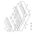
- A plasma display panel having a first group of parallel electrodes (6,14) and a second group of parallel electrodes (7,13) and comprising a front glass plate (1), a back plate (5) and a diaphragm (3,4) therebetween, said front glass plate (1) and said back plate (5) being sealed together, said diaphragm (3,4) having an upper surface and a lower surface and consisting of a metallic sheet having a plurality of aperures for permitting discharge, said apertures being filled with an ionizable gas,
characterized in that the electrodes (6,14) of the first group and the electrodes (7,13) of the second group are situated in parallel planes, which have a predetermined distance, and in a vertical view of the plasma display the electrodes of the first group and the second group intersect, said diaphragm (3,4) has a thickness of 0.01 to 1.0 mm, at least one of said upper and lower surfaces of said diaphragm (3,4) is provided with a dielectric coating (2) consisting of a dielectric material in a glass, the minimum pitch in the arrangement of said apertures is less than 0.6mm. - A plasma display panel having a first group of parallel electrodes (6,14) and a second group of parallel electrodes (7, 13) and comprising a front glass plate (1), a back plate (5) and a diaphragm (3,4) therebetween, said front glass plate (1) and said back plate (5) being sealed together, said diaphragm (3,4) having an upper surface and a lower surface and consisting of a metallic sheet having a plurality of apertures for permitting discharge, said apertures being filled with an ionizable gas,
characterized in that the electrodes (6,14) of the first group and the electrodes (7,13) of the second group are situated in parallel planes, which have a predetermined distance, and in a vertical view of the plasma display the electrodes of the first group and the second group intersect, at least one of said upper and lower surfaces of said diaphragm (3,4) is provided with a dielectric coating (2) consisting of a dielectric material in a glass, and said diaphragm (3,4) is used as a discharge electrode in addition to said first and second groups of parallel electrodes. - A plasma display panel according to claim 1 or 2, charcterized in that said metallic sheet contains at least one metal selected from the group consisting of iron, nickel, chromium and cobalt, and has a coefficient of linear expansion of 40 x 10-7/°C to 100 x 10-7/°C at 25 to 500°C.
- A plasma display panel according to claim 1 or 2, characterized in that said glass in said dielectric layer (2) has a softening point of 350 to 1000°C.
- A plasma display panel according to claim 1 or 2, characterized in that said dielectric layer (2) has a thickness of 2 to 40µm.
- A plasma display panel according to claim 1 or 2, characterized in that said metallic sheet comprises a plurality of stacked metal sheets having apertures overlapped on the same position.
- A plasma display panel according to claim 1 or 2, characterized in that said apertures have an inner surface and a fluorescent material (11) is deposited on said inner surface of said apertures.
- A method of producing a plasma display panel comprising a back plate (1) provided with a first group of parallel electrodes (6,14), a diaphragm (3,4) having a thickness of 0.01 to 1.0 mm and a front glass plate (1) provided with a second group of parallel electrodes (7,13) hermetically sealed together, wherein the electrodes (6,14) of the first group and the electrodes (7,13) of the second group are situated in parallel planes, which have a predetermined distance, and in a vertical view of the plasma display the electrodes of the first group and the second group intersect, said diaphragm (3,4) consisting of at least one metal sheet having a plurality of apertures of discharge cells which are located where said electrodes, in a vertical view, intersect, at least one of said upper and lower surfaces of said diaphragm (3,4) being provided with a dielectric coating (2) consisting of a dielectric material in a glass, the minimum pitch of the arrangement of said apertures being less than 0.6mm,
characterized in that a glass and a dielectric powder including the glass is electrodeposited on the surface of the metal sheet, using the metal sheet as an electrode in a solution containing an electrolyte in which said glass and said dielectric powder including the glass is suspended, and followed by heating to melt the glass, so that the dielectric layer electrically insulates the metal sheet and the two groups of parallel electrodes are firmly adhered onto the metal sheet. - A method of producing a plasma display panel comprising a back plate (1) provided with a first group of parallel electrodes (6,14), a diaphragm (3,4) having a thickness of 0.01 to 1.0 mm and a front glass plate (1) provided with a second group of parallel electrodes (7,13) hermetically sealed together, wherein the electrodes (6,14) of the first group and the electrodes (7,13) of the second group are situated in parallel planes, which have a predetermined distance, and in a vertical view of the plasma display the electrodes of the first group and the second group intersect, said diaphragm (3,4) consisting of at least one metal sheet having a plurality of apertures of discharge cells which are located where said electrodes, in a vertical view, intersect, at least one of said upper and lower surfaces of said diaphragm (3,4) being provided with a dielectric coating (2) consisting of a dielectric material in a glass, the minimum pitch of the arrangement of said apertures being less than 0./6mm,
characterized in that the method comprises the steps of coating a mixture of a glass and a dielectric powder including the glass, an organic polymer and a solvent on a stripable substrate to form the dielectric layer (2), applying the dielectric layer (2) on said substrate to one or both surfaces of said metal sheet by pressure and/or heating together, stripping said substrate to transfer the dielectric layer (2) to the surface of said metal sheet, and heating to melt said glass and to remove the organic polymer and the solvent, so that the dielectric layer (2) electrically insulates the metal sheet and the two groups of parallel electrodes are firmly adhered onto the metal sheet.
Applications Claiming Priority (15)
| Application Number | Priority Date | Filing Date | Title |
|---|---|---|---|
| JP26915389 | 1989-10-18 | ||
| JP269153/89 | 1989-10-18 | ||
| JP1290027A JPH0770288B2 (en) | 1989-11-09 | 1989-11-09 | Gas discharge type panel |
| JP290027/89 | 1989-11-09 | ||
| JP25981/90 | 1990-02-07 | ||
| JP2025981A JP2741418B2 (en) | 1989-10-18 | 1990-02-07 | Metal core rib, method of manufacturing the same, and plasma display panel using the metal core rib |
| JP2027193A JPH03233832A (en) | 1990-02-08 | 1990-02-08 | Plasma display panel comprising porous metal plate as common cathode |
| JP27193/90 | 1990-02-08 | ||
| JP120048/90 | 1990-05-11 | ||
| JP2120048A JP2532970B2 (en) | 1990-05-11 | 1990-05-11 | Plasma display panel using perforated metal plate as partition wall and method of manufacturing the same |
| JP247433/90 | 1990-09-19 | ||
| JP2247433A JP2525280B2 (en) | 1990-09-19 | 1990-09-19 | Plasma display panel using perforated metal plate in partition as electrode |
| JP2270610A JPH04147535A (en) | 1990-10-11 | 1990-10-11 | Method of forming insulating layer of porous metal plate |
| JP270610/90 | 1990-10-11 | ||
| PCT/JP1990/001338 WO1991006115A1 (en) | 1989-10-18 | 1990-10-17 | Plasma display panel and method of manufacturing the same |
Publications (3)
| Publication Number | Publication Date |
|---|---|
| EP0448727A1 EP0448727A1 (en) | 1991-10-02 |
| EP0448727A4 EP0448727A4 (en) | 1992-12-09 |
| EP0448727B1 true EP0448727B1 (en) | 1998-01-28 |
Family
ID=27564084
Family Applications (1)
| Application Number | Title | Priority Date | Filing Date |
|---|---|---|---|
| EP90915195A Expired - Lifetime EP0448727B1 (en) | 1989-10-18 | 1990-10-17 | Plasma display panel and method of manufacturing the same |
Country Status (7)
| Country | Link |
|---|---|
| US (1) | US5264758A (en) |
| EP (1) | EP0448727B1 (en) |
| AT (1) | ATE162907T1 (en) |
| AU (1) | AU638288B2 (en) |
| CA (1) | CA2044267C (en) |
| DE (1) | DE69032003T2 (en) |
| WO (1) | WO1991006115A1 (en) |
Families Citing this family (32)
| Publication number | Priority date | Publication date | Assignee | Title |
|---|---|---|---|---|
| JP2593761B2 (en) * | 1992-02-06 | 1997-03-26 | 株式会社ノリタケカンパニーリミテド | Plasma display panel |
| US5672460A (en) * | 1994-06-10 | 1997-09-30 | Nippon Hoso Kyokai | Method for forming conductive or insulating layers |
| JP2663915B2 (en) * | 1995-05-31 | 1997-10-15 | 日本電気株式会社 | Plasma display panel |
| US6373452B1 (en) * | 1995-08-03 | 2002-04-16 | Fujiitsu Limited | Plasma display panel, method of driving same and plasma display apparatus |
| TW353762B (en) * | 1996-10-21 | 1999-03-01 | Dainippon Printing Co Ltd | Transfer sheet, and pattern-forming method |
| US6159066A (en) * | 1996-12-18 | 2000-12-12 | Fujitsu Limited | Glass material used in, and fabrication method of, a plasma display panel |
| KR100406785B1 (en) * | 1997-05-22 | 2004-01-24 | 삼성에스디아이 주식회사 | Plasma display panel and manufacturing mehtod the same |
| JP3520396B2 (en) * | 1997-07-02 | 2004-04-19 | セイコーエプソン株式会社 | Active matrix substrate and display device |
| WO1999010862A1 (en) | 1997-08-21 | 1999-03-04 | Seiko Epson Corporation | Active matrix display |
| JP3580092B2 (en) * | 1997-08-21 | 2004-10-20 | セイコーエプソン株式会社 | Active matrix display |
| TW392186B (en) * | 1997-12-01 | 2000-06-01 | Hitachi Ltd | Plasma display panel and image display using the same |
| US6286204B1 (en) * | 1998-03-09 | 2001-09-11 | Sarnoff Corporation | Method for fabricating double sided ceramic circuit boards using a titanium support substrate |
| US6184163B1 (en) * | 1998-03-26 | 2001-02-06 | Lg Electronics Inc. | Dielectric composition for plasma display panel |
| US6439943B1 (en) * | 1998-05-12 | 2002-08-27 | Matsushita Electric Industrial Co., Ltd. | Manufacturing method of plasma display panel that includes adielectric glass layer having small particle sizes |
| KR100662061B1 (en) * | 1998-09-29 | 2006-12-27 | 가부시끼가이샤 히다치 세이사꾸쇼 | Method of manufacturing plasma display and substrate structure |
| CN1108599C (en) * | 1999-08-03 | 2003-05-14 | 东南大学 | Plasma display board |
| JP2002287694A (en) * | 2001-03-26 | 2002-10-04 | Hitachi Ltd | Method for driving plasma display panel, driving circuit and picture display device |
| JP4177969B2 (en) * | 2001-04-09 | 2008-11-05 | 株式会社日立製作所 | Plasma display panel |
| US7067979B2 (en) * | 2001-10-02 | 2006-06-27 | Noritake Co., Limited | Gas-discharge display device and its manufacturing method |
| KR100444512B1 (en) * | 2002-01-25 | 2004-08-16 | 엘지전자 주식회사 | Method For Removing Impurities Of Plasma Display Panel |
| TW540746U (en) * | 2002-07-18 | 2003-07-01 | Delta Optoelectronics Inc | Vacuum device |
| US6825609B2 (en) * | 2002-10-21 | 2004-11-30 | Hon Hai Precision Ind. Co., Ltd. | Sealed housing for field emission display |
| JP2004179052A (en) * | 2002-11-28 | 2004-06-24 | Pioneer Electronic Corp | Display panel, its manufacturing method and partition wall for display panel |
| KR100932975B1 (en) * | 2003-03-27 | 2009-12-21 | 삼성에스디아이 주식회사 | Field emission display device with multi-layered grid plate |
| KR20040087905A (en) * | 2003-04-09 | 2004-10-15 | 파이오니아 가부시키가이샤 | Plasma display panel |
| KR100525888B1 (en) * | 2003-06-23 | 2005-11-02 | 엘지전자 주식회사 | Paste composites for white-back formation and method for manufacturing a lower substrate in the plasma display panel |
| KR20050096532A (en) * | 2004-03-31 | 2005-10-06 | 삼성에스디아이 주식회사 | Electron emission device and electron emission display using the same |
| JP2005339944A (en) * | 2004-05-26 | 2005-12-08 | Pioneer Electronic Corp | Plasma display panel |
| JP4401905B2 (en) * | 2004-09-03 | 2010-01-20 | 株式会社日立製作所 | Plasma display panel and image display system using the same. |
| KR100683749B1 (en) | 2005-01-05 | 2007-02-15 | 삼성에스디아이 주식회사 | Chassis base for plasma display apparatus and plasma display apparatus comprising the same |
| US20060290256A1 (en) * | 2005-01-31 | 2006-12-28 | Tdk Corporation | Panel |
| KR20060095331A (en) * | 2005-02-28 | 2006-08-31 | 삼성에스디아이 주식회사 | Electron emission device |
Citations (1)
| Publication number | Priority date | Publication date | Assignee | Title |
|---|---|---|---|---|
| EP0012140A1 (en) * | 1978-12-15 | 1980-06-25 | International Business Machines Corporation | Gaseous discharge display devices |
Family Cites Families (10)
| Publication number | Priority date | Publication date | Assignee | Title |
|---|---|---|---|---|
| JPS4751538B1 (en) * | 1968-10-09 | 1972-12-25 | ||
| US3842308A (en) * | 1970-12-12 | 1974-10-15 | Philips Corp | Gas discharge panel with apertured center plate having an oxidized surface |
| FR2134895A5 (en) * | 1971-04-23 | 1972-12-08 | Thomson Csf | |
| JPS5511262B2 (en) * | 1974-05-21 | 1980-03-24 | ||
| GB1509487A (en) * | 1976-01-08 | 1978-05-04 | Ibm | Gas panel display devices |
| JPS5351538A (en) * | 1976-10-21 | 1978-05-11 | Toshihiko Sakurai | Device for tracing sun |
| CA1114000A (en) * | 1977-10-11 | 1981-12-08 | Charles H. Perry | Gas panel spacer |
| JPS5826772B2 (en) * | 1978-08-18 | 1983-06-04 | 松下電器産業株式会社 | Control electrode of image display device |
| NL7907489A (en) * | 1979-10-10 | 1981-04-14 | Philips Nv | GAS DISCHARGE IMAGE DISPLAY PANEL WITH HOLLOW CATHODS. |
| US4352040A (en) * | 1980-07-14 | 1982-09-28 | Burroughs Corporation | Display panel with anode and cathode electrodes located in slots of base plate |
-
1990
- 1990-10-17 AU AU65318/90A patent/AU638288B2/en not_active Ceased
- 1990-10-17 AT AT90915195T patent/ATE162907T1/en not_active IP Right Cessation
- 1990-10-17 US US07/690,924 patent/US5264758A/en not_active Expired - Fee Related
- 1990-10-17 DE DE69032003T patent/DE69032003T2/en not_active Expired - Fee Related
- 1990-10-17 WO PCT/JP1990/001338 patent/WO1991006115A1/en active IP Right Grant
- 1990-10-17 EP EP90915195A patent/EP0448727B1/en not_active Expired - Lifetime
- 1990-10-17 CA CA002044267A patent/CA2044267C/en not_active Expired - Fee Related
Patent Citations (1)
| Publication number | Priority date | Publication date | Assignee | Title |
|---|---|---|---|---|
| EP0012140A1 (en) * | 1978-12-15 | 1980-06-25 | International Business Machines Corporation | Gaseous discharge display devices |
Also Published As
| Publication number | Publication date |
|---|---|
| CA2044267A1 (en) | 1991-04-19 |
| EP0448727A1 (en) | 1991-10-02 |
| DE69032003D1 (en) | 1998-03-05 |
| ATE162907T1 (en) | 1998-02-15 |
| EP0448727A4 (en) | 1992-12-09 |
| AU638288B2 (en) | 1993-06-24 |
| CA2044267C (en) | 1999-04-20 |
| WO1991006115A1 (en) | 1991-05-02 |
| US5264758A (en) | 1993-11-23 |
| AU6531890A (en) | 1991-05-16 |
| DE69032003T2 (en) | 1998-06-18 |
Similar Documents
| Publication | Publication Date | Title |
|---|---|---|
| EP0448727B1 (en) | Plasma display panel and method of manufacturing the same | |
| US5747931A (en) | Plasma display and method of making same | |
| EP0784333B1 (en) | Gas discharging type display panel and manufacturing method thereof | |
| JP3583144B2 (en) | Plasma display and method of manufacturing the same | |
| KR0138075B1 (en) | Plasma display panel | |
| KR930004994B1 (en) | Plasma display paneled of manufacturing | |
| JP2741418B2 (en) | Metal core rib, method of manufacturing the same, and plasma display panel using the metal core rib | |
| US5836798A (en) | Method of making a plasma display panel | |
| JP2532970B2 (en) | Plasma display panel using perforated metal plate as partition wall and method of manufacturing the same | |
| US7719191B2 (en) | Plasma display panel | |
| JP2525280B2 (en) | Plasma display panel using perforated metal plate in partition as electrode | |
| US20090091236A1 (en) | Plasma display panel having alignment structures and method of fabricating the same | |
| EP0124099A2 (en) | Display panel and method of making it | |
| US3849686A (en) | Plasma display panel comprising a first external electrode for each digit and a second external electrode for each segment | |
| JPH04147535A (en) | Method of forming insulating layer of porous metal plate | |
| JPH05225911A (en) | Plasma display panel | |
| KR950006104B1 (en) | Mehtod of forming electrode of discharge display device | |
| KR100361955B1 (en) | Ac plasma display panel | |
| JPH03152830A (en) | Gas discharging type panel | |
| JPH11162362A (en) | Manufacture of plasma display panel | |
| KR800000296B1 (en) | Flat panel display apparatus | |
| JPH05266803A (en) | Plasma display panel | |
| JPH05174715A (en) | Color plasma display panel | |
| JPH0320932A (en) | Plasma display panel | |
| JPH0495330A (en) | Gas electric discharge panel |
Legal Events
| Date | Code | Title | Description |
|---|---|---|---|
| PUAI | Public reference made under article 153(3) epc to a published international application that has entered the european phase |
Free format text: ORIGINAL CODE: 0009012 |
|
| 17P | Request for examination filed |
Effective date: 19910613 |
|
| AK | Designated contracting states |
Kind code of ref document: A1 Designated state(s): AT BE CH DE ES FR GB GR IT LI LU NL SE |
|
| A4 | Supplementary search report drawn up and despatched |
Effective date: 19921022 |
|
| AK | Designated contracting states |
Kind code of ref document: A4 Designated state(s): AT BE CH DE ES FR GB GR IT LI LU NL SE |
|
| 17Q | First examination report despatched |
Effective date: 19940701 |
|
| APCB | Communication from the board of appeal sent |
Free format text: ORIGINAL CODE: EPIDOS OBAPE |
|
| APAU | Communication from the board of appeal sent |
Free format text: ORIGINAL CODE: EPIDOS OBAP |
|
| APCB | Communication from the board of appeal sent |
Free format text: ORIGINAL CODE: EPIDOS OBAPE |
|
| APCB | Communication from the board of appeal sent |
Free format text: ORIGINAL CODE: EPIDOS OBAPE |
|
| APCB | Communication from the board of appeal sent |
Free format text: ORIGINAL CODE: EPIDOS OBAPE |
|
| APCB | Communication from the board of appeal sent |
Free format text: ORIGINAL CODE: EPIDOS OBAPE |
|
| APAB | Appeal dossier modified |
Free format text: ORIGINAL CODE: EPIDOS NOAPE |
|
| GRAG | Despatch of communication of intention to grant |
Free format text: ORIGINAL CODE: EPIDOS AGRA |
|
| GRAH | Despatch of communication of intention to grant a patent |
Free format text: ORIGINAL CODE: EPIDOS IGRA |
|
| GRAH | Despatch of communication of intention to grant a patent |
Free format text: ORIGINAL CODE: EPIDOS IGRA |
|
| GRAA | (expected) grant |
Free format text: ORIGINAL CODE: 0009210 |
|
| AK | Designated contracting states |
Kind code of ref document: B1 Designated state(s): AT BE CH DE ES FR GB GR IT LI LU NL SE |
|
| PG25 | Lapsed in a contracting state [announced via postgrant information from national office to epo] |
Ref country code: IT Free format text: LAPSE BECAUSE OF FAILURE TO SUBMIT A TRANSLATION OF THE DESCRIPTION OR TO PAY THE FEE WITHIN THE PRESCRIBED TIME-LIMIT;WARNING: LAPSES OF ITALIAN PATENTS WITH EFFECTIVE DATE BEFORE 2007 MAY HAVE OCCURRED AT ANY TIME BEFORE 2007. THE CORRECT EFFECTIVE DATE MAY BE DIFFERENT FROM THE ONE RECORDED. Effective date: 19980128 Ref country code: GR Free format text: LAPSE BECAUSE OF FAILURE TO SUBMIT A TRANSLATION OF THE DESCRIPTION OR TO PAY THE FEE WITHIN THE PRESCRIBED TIME-LIMIT Effective date: 19980128 Ref country code: ES Free format text: THE PATENT HAS BEEN ANNULLED BY A DECISION OF A NATIONAL AUTHORITY Effective date: 19980128 Ref country code: CH Free format text: LAPSE BECAUSE OF FAILURE TO SUBMIT A TRANSLATION OF THE DESCRIPTION OR TO PAY THE FEE WITHIN THE PRESCRIBED TIME-LIMIT Effective date: 19980128 Ref country code: BE Free format text: LAPSE BECAUSE OF FAILURE TO SUBMIT A TRANSLATION OF THE DESCRIPTION OR TO PAY THE FEE WITHIN THE PRESCRIBED TIME-LIMIT Effective date: 19980128 Ref country code: LI Free format text: LAPSE BECAUSE OF FAILURE TO SUBMIT A TRANSLATION OF THE DESCRIPTION OR TO PAY THE FEE WITHIN THE PRESCRIBED TIME-LIMIT Effective date: 19980128 Ref country code: AT Free format text: LAPSE BECAUSE OF FAILURE TO SUBMIT A TRANSLATION OF THE DESCRIPTION OR TO PAY THE FEE WITHIN THE PRESCRIBED TIME-LIMIT Effective date: 19980128 |
|
| REF | Corresponds to: |
Ref document number: 162907 Country of ref document: AT Date of ref document: 19980215 Kind code of ref document: T |
|
| REG | Reference to a national code |
Ref country code: CH Ref legal event code: EP |
|
| REF | Corresponds to: |
Ref document number: 69032003 Country of ref document: DE Date of ref document: 19980305 |
|
| ET | Fr: translation filed | ||
| PG25 | Lapsed in a contracting state [announced via postgrant information from national office to epo] |
Ref country code: SE Free format text: LAPSE BECAUSE OF FAILURE TO SUBMIT A TRANSLATION OF THE DESCRIPTION OR TO PAY THE FEE WITHIN THE PRESCRIBED TIME-LIMIT Effective date: 19980428 |
|
| REG | Reference to a national code |
Ref country code: CH Ref legal event code: PL |
|
| PGFP | Annual fee paid to national office [announced via postgrant information from national office to epo] |
Ref country code: FR Payment date: 19980827 Year of fee payment: 9 |
|
| PGFP | Annual fee paid to national office [announced via postgrant information from national office to epo] |
Ref country code: NL Payment date: 19980828 Year of fee payment: 9 |
|
| PGFP | Annual fee paid to national office [announced via postgrant information from national office to epo] |
Ref country code: GB Payment date: 19981009 Year of fee payment: 9 |
|
| PG25 | Lapsed in a contracting state [announced via postgrant information from national office to epo] |
Ref country code: LU Free format text: LAPSE BECAUSE OF NON-PAYMENT OF DUE FEES Effective date: 19981017 |
|
| PLBE | No opposition filed within time limit |
Free format text: ORIGINAL CODE: 0009261 |
|
| STAA | Information on the status of an ep patent application or granted ep patent |
Free format text: STATUS: NO OPPOSITION FILED WITHIN TIME LIMIT |
|
| PGFP | Annual fee paid to national office [announced via postgrant information from national office to epo] |
Ref country code: DE Payment date: 19981208 Year of fee payment: 9 |
|
| 26N | No opposition filed | ||
| PG25 | Lapsed in a contracting state [announced via postgrant information from national office to epo] |
Ref country code: GB Free format text: LAPSE BECAUSE OF NON-PAYMENT OF DUE FEES Effective date: 19991017 |
|
| PG25 | Lapsed in a contracting state [announced via postgrant information from national office to epo] |
Ref country code: NL Free format text: LAPSE BECAUSE OF NON-PAYMENT OF DUE FEES Effective date: 20000501 |
|
| GBPC | Gb: european patent ceased through non-payment of renewal fee |
Effective date: 19991017 |
|
| PG25 | Lapsed in a contracting state [announced via postgrant information from national office to epo] |
Ref country code: FR Free format text: LAPSE BECAUSE OF NON-PAYMENT OF DUE FEES Effective date: 20000630 |
|
| NLV4 | Nl: lapsed or anulled due to non-payment of the annual fee |
Effective date: 20000501 |
|
| PG25 | Lapsed in a contracting state [announced via postgrant information from national office to epo] |
Ref country code: DE Free format text: LAPSE BECAUSE OF NON-PAYMENT OF DUE FEES Effective date: 20000801 |
|
| REG | Reference to a national code |
Ref country code: FR Ref legal event code: ST |
|
| APAH | Appeal reference modified |
Free format text: ORIGINAL CODE: EPIDOSCREFNO |