JP4401905B2 - Plasma display panel and image display system using the same. - Google Patents
Plasma display panel and image display system using the same. Download PDFInfo
- Publication number
- JP4401905B2 JP4401905B2 JP2004257253A JP2004257253A JP4401905B2 JP 4401905 B2 JP4401905 B2 JP 4401905B2 JP 2004257253 A JP2004257253 A JP 2004257253A JP 2004257253 A JP2004257253 A JP 2004257253A JP 4401905 B2 JP4401905 B2 JP 4401905B2
- Authority
- JP
- Japan
- Prior art keywords
- discharge
- display panel
- plasma display
- front substrate
- space
- Prior art date
- Legal status (The legal status is an assumption and is not a legal conclusion. Google has not performed a legal analysis and makes no representation as to the accuracy of the status listed.)
- Expired - Fee Related
Links
Images


Classifications
-
- H—ELECTRICITY
- H01—ELECTRIC ELEMENTS
- H01J—ELECTRIC DISCHARGE TUBES OR DISCHARGE LAMPS
- H01J11/00—Gas-filled discharge tubes with alternating current induction of the discharge, e.g. alternating current plasma display panels [AC-PDP]; Gas-filled discharge tubes without any main electrode inside the vessel; Gas-filled discharge tubes with at least one main electrode outside the vessel
- H01J11/20—Constructional details
- H01J11/34—Vessels, containers or parts thereof, e.g. substrates
- H01J11/42—Fluorescent layers
-
- H—ELECTRICITY
- H01—ELECTRIC ELEMENTS
- H01J—ELECTRIC DISCHARGE TUBES OR DISCHARGE LAMPS
- H01J1/00—Details of electrodes, of magnetic control means, of screens, or of the mounting or spacing thereof, common to two or more basic types of discharge tubes or lamps
- H01J1/88—Mounting, supporting, spacing, or insulating of electrodes or of electrode assemblies
-
- H—ELECTRICITY
- H01—ELECTRIC ELEMENTS
- H01J—ELECTRIC DISCHARGE TUBES OR DISCHARGE LAMPS
- H01J11/00—Gas-filled discharge tubes with alternating current induction of the discharge, e.g. alternating current plasma display panels [AC-PDP]; Gas-filled discharge tubes without any main electrode inside the vessel; Gas-filled discharge tubes with at least one main electrode outside the vessel
- H01J11/20—Constructional details
- H01J11/34—Vessels, containers or parts thereof, e.g. substrates
- H01J11/36—Spacers, barriers, ribs, partitions or the like
-
- H—ELECTRICITY
- H01—ELECTRIC ELEMENTS
- H01J—ELECTRIC DISCHARGE TUBES OR DISCHARGE LAMPS
- H01J11/00—Gas-filled discharge tubes with alternating current induction of the discharge, e.g. alternating current plasma display panels [AC-PDP]; Gas-filled discharge tubes without any main electrode inside the vessel; Gas-filled discharge tubes with at least one main electrode outside the vessel
- H01J11/20—Constructional details
- H01J11/34—Vessels, containers or parts thereof, e.g. substrates
- H01J11/44—Optical arrangements or shielding arrangements, e.g. filters, black matrices, light reflecting means or electromagnetic shielding means
-
- H—ELECTRICITY
- H01—ELECTRIC ELEMENTS
- H01J—ELECTRIC DISCHARGE TUBES OR DISCHARGE LAMPS
- H01J17/00—Gas-filled discharge tubes with solid cathode
- H01J17/38—Cold-cathode tubes
- H01J17/48—Cold-cathode tubes with more than one cathode or anode, e.g. sequence-discharge tube, counting tube, dekatron
- H01J17/49—Display panels, e.g. with crossed electrodes, e.g. making use of direct current
- H01J17/492—Display panels, e.g. with crossed electrodes, e.g. making use of direct current with crossed electrodes
-
- H—ELECTRICITY
- H01—ELECTRIC ELEMENTS
- H01J—ELECTRIC DISCHARGE TUBES OR DISCHARGE LAMPS
- H01J2211/00—Plasma display panels with alternate current induction of the discharge, e.g. AC-PDPs
- H01J2211/20—Constructional details
- H01J2211/34—Vessels, containers or parts thereof, e.g. substrates
- H01J2211/36—Spacers, barriers, ribs, partitions or the like
- H01J2211/361—Spacers, barriers, ribs, partitions or the like characterized by the shape
-
- H—ELECTRICITY
- H01—ELECTRIC ELEMENTS
- H01J—ELECTRIC DISCHARGE TUBES OR DISCHARGE LAMPS
- H01J2211/00—Plasma display panels with alternate current induction of the discharge, e.g. AC-PDPs
- H01J2211/20—Constructional details
- H01J2211/34—Vessels, containers or parts thereof, e.g. substrates
- H01J2211/44—Optical arrangements or shielding arrangements, e.g. filters or lenses
- H01J2211/442—Light reflecting means; Anti-reflection means
-
- H—ELECTRICITY
- H01—ELECTRIC ELEMENTS
- H01J—ELECTRIC DISCHARGE TUBES OR DISCHARGE LAMPS
- H01J2211/00—Plasma display panels with alternate current induction of the discharge, e.g. AC-PDPs
- H01J2211/20—Constructional details
- H01J2211/34—Vessels, containers or parts thereof, e.g. substrates
- H01J2211/44—Optical arrangements or shielding arrangements, e.g. filters or lenses
- H01J2211/444—Means for improving contrast or colour purity, e.g. black matrix or light shielding means
Description
本発明はプラズマディスプレイパネル(Plasma Display Panel:以下、プラズマパネルまたはPDPとも称する)に関し、特に、明室コントラストを向上させ、かつ高効率で高画質化を実現できるプラズマパネル構造とその製造方法、その駆動方法、および駆動装置を含めたプラズマディスプレイ装置に関する。 The present invention relates to a plasma display panel (hereinafter also referred to as plasma panel or PDP), and in particular, a plasma panel structure capable of improving bright room contrast and realizing high image quality with high efficiency, and a method for manufacturing the same The present invention relates to a driving method and a plasma display device including the driving device.
近年、大型かつ厚みに薄いカラー表示装置として、プラズマディスプレイ装置が期待されている。特に、表示放電を同一基板上に設けられた電極間で発生させ、且つ交流駆動される、交流(AC)面内放電型PDPは、構造の単純さと高信頼性のため、もっとも実用化の進んでいる方式である。以下、従来技術のAC面内放電型PDPの実施形態を説明する。 In recent years, a plasma display device is expected as a large and thin color display device. In particular, an alternating current (AC) in-plane discharge type PDP that generates display discharge between electrodes provided on the same substrate and is driven by alternating current is most practically used because of its simple structure and high reliability. This method Hereinafter, embodiments of a conventional AC in-plane discharge type PDP will be described.
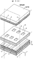
図1は、プラズマパネルの構造の一部を示す分解斜視図であり、前面ガラス基板1(後に説明する視野空間側の基板)の下面には透明な共通電極(以降X電極と称す)22-1乃至22-2と、透明な独立電極(以降Y電極または走査電極と称す)23-1乃至23-2を付設する。また、X電極22-1乃至22-2とY電極23-1乃至23-2には、それぞれXバス電極24-1乃至24-2とYバス電極25-1乃至25-2を積層付設する。さらに、X電極22-1乃至22-2、Y電極23-1乃至23-2、Xバス電極24-1乃至24-2、Yバス電極25-1乃至25-2を誘電体2によって被覆し、酸化マグネシウム(MgO)等の保護膜(保護層ともいう)3を付設する。X電極22-1乃至22-2、Y電極23-1乃至23-2、Xバス電極24-1乃至24-2、Yバス電極25-1乃至25-2をまとめて表示放電電極または表示電極(XとYの対の概念を含む時は表示放電電極対または表示電極対)と総称する。また、上記ではX電極22-1乃至22-2、Y電極23-1乃至23-2を透明電極と説明したが、この方が明るい(輝度の大きな)プラズマパネルができるからであり、必ずしも透明である必要はないことは言うまでもない。また、保護膜3の材料として酸化マグネシウム(MgO)を具体的に示したが、必ずしもこれである必要はない。保護膜3の目的は、入射するイオンから表示放電電極と誘電体2を保護することと、イオン入射に伴う2次電子放出により放電発生と放電継続を支援することであり、このような目的を達することが出来れば他の材料であっても構わない。このようにして一体加工したものを前面板と呼ぶ。
FIG. 1 is an exploded perspective view showing a part of the structure of a plasma panel. A transparent common electrode (hereinafter referred to as an X electrode) 22- is formed on the lower surface of a front glass substrate 1 (a substrate on the viewing space side described later). 1 to 22-2 and transparent independent electrodes (hereinafter referred to as Y electrodes or scanning electrodes) 23-1 to 23-2 are provided. Further, the X bus electrodes 24-1 to 24-2 and the Y bus electrodes 25-1 to 25-2 are stacked on the X electrodes 22-1 to 22-2 and the Y electrodes 23-1 to 23-2, respectively. . Furthermore, the X electrodes 22-1 to 22-2, the Y electrodes 23-1 to 23-2, the X bus electrodes 24-1 to 24-2 and the Y bus electrodes 25-1 to 25-2 are covered with the dielectric 2. A protective film (also called a protective layer) 3 such as magnesium oxide (MgO) is attached. Display electrodes or display electrodes collectively including X electrodes 22-1 to 22-2, Y electrodes 23-1 to 23-2, X bus electrodes 24-1 to 24-2, and Y bus electrodes 25-1 to 25-2 (When the concept of X and Y pair is included, it is generally called a display discharge electrode pair or a display electrode pair). In the above description, the X electrodes 22-1 to 22-2 and the Y electrodes 23-1 to 23-2 have been described as transparent electrodes. However, this is because a brighter (higher luminance) plasma panel can be formed, which is not necessarily transparent. Needless to say, there is no need. Further, although magnesium oxide (MgO) is specifically shown as the material of the
一方、背面ガラス基板10の上面には、X電極22-1乃至22-2、Y電極23-1乃至23-2と直角に立体交差する電極(以降A電極またはアドレス電極と称す)11を付設し、該A電極11を誘電体9によって被覆し、該誘電体9の上に隔壁7をA電極11と平行に設ける。さらに、隔壁7の壁面と誘電体9の上面によって形成される凹領域の内側に蛍光体8を塗布する。このようにして一体加工したものを背面板と呼ぶ。
On the other hand, on the upper surface of the
上記のように必要な構成要素を作り込んだ前面板と背面板を接合し、プラズマを生成するためのガス(放電ガス)を充填し、封止してプラズマパネルが形成される。上記前面、背面基板の接合および封止において上記放電ガスの気密性が保持される必要があることは言うまでもない。 A front panel and a rear panel in which necessary components are formed as described above are joined, filled with a gas (discharge gas) for generating plasma, and sealed to form a plasma panel. Needless to say, the airtightness of the discharge gas needs to be maintained in the bonding and sealing of the front and back substrates.
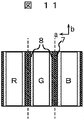
図2は図1中の矢印bの方向から見たPDPの断面図であり、1画素の最小単位であるセル3個を概略示している。セルの境界は概略破線で示す位置である。以下、セルのことを放電セルとも呼ぶ。 FIG. 2 is a cross-sectional view of the PDP as viewed from the direction of the arrow b in FIG. 1, and schematically shows three cells that are the minimum unit of one pixel. The cell boundary is a position indicated by a broken line. Hereinafter, the cell is also referred to as a discharge cell.
図2より、A電極11は2つの隔壁7の中間に位置し前面ガラス基板1と背面ガラス基板10、隔壁7に囲まれた放電空間12には上記プラズマを生成するためのガス(放電ガス)が充填されている。
As shown in FIG. 2, the
なお、放電空間とはプラズマパネルの駆動において、後に述べる表示放電、書き込み放電、予備放電(リセット放電とも称す)のいずれかの発生する空間のことである。さらに、具体的には、上記放電ガスが満たされ、上記放電に必要な電界が印加され、放電発生に必要な空間的広がりを有する空間である。さらに、表示放電の発生する空間(具体的には、上記放電ガスが満たされ、表示放電に必要な電界が印加され、表示放電発生に必要な空間的広がりを有する空間)を表示放電空間と呼ぶ。放電空間および表示放電空間は、個々の放電セルに含まれる空間を意味する場合もあるし、これら空間の集合を意味する場合もある。 Note that the discharge space is a space where any one of display discharge, writing discharge, and preliminary discharge (also referred to as reset discharge) described later occurs in driving the plasma panel. More specifically, it is a space that is filled with the discharge gas, is applied with an electric field necessary for the discharge, and has a spatial extent necessary for generating the discharge. Furthermore, a space in which display discharge occurs (specifically, a space that is filled with the discharge gas, an electric field necessary for display discharge is applied, and has a spatial extent necessary for display discharge generation) is referred to as a display discharge space. . The discharge space and the display discharge space may mean a space included in each discharge cell or a set of these spaces.
カラーPDPでは、通常セル内に塗布する蛍光体には、赤、緑、青用の3種類がある。この3種類の別々の蛍光体を塗布した3セルをまとめて1画素とする。このようなセル、または画素が複数個連続的かつ周期的に集合した空間を表示空間と呼ぶ。このような表示空間を含み真空封着機能、電極取り出し機能等他の必要な機能を有するものをプラズマディスプレイパネルまたはプラズマパネルと呼ぶ。以下、プラズマパネルをPDPとも記す。 In the color PDP, there are usually three types of phosphors for red, green, and blue that are applied in a cell. Three cells coated with these three kinds of separate phosphors are collectively set as one pixel. A space in which a plurality of such cells or pixels are gathered continuously and periodically is called a display space. A device including such a display space and having other necessary functions such as a vacuum sealing function and an electrode extraction function is called a plasma display panel or a plasma panel. Hereinafter, the plasma panel is also referred to as PDP.
上記プラズマパネルにおいて、上記放電ガスの気密性を保持して一体不可分の構成部を基本プラズマパネルと称す。上記基本プラズマパネルにおいて、表示用の可視光を放射する面を表示面とし、上記表示用の可視光が放射される空間を視野空間とする。上述した如く、上記基本プラズマパネルにおいて少なくとも複数の上記放電セルを連続的に包含する空間が存在し、これを表示空間とする。前記複数個の放電セルの一つによって占められる空間を、前記前面基板へ投影した時に得られる面積をS1とし、該放電セルの一つからの前記可視光を前記前面基板の外に出射する、前記前面基板における窓部の面積をS2としたとき、S2/S1を表示放電領域の面積率(開口率)とする。また、S2以外の面、すなわち、S2−S1を非開口面と呼び、その面積率(S2−S1)/S1を非開口率と呼ぶ。 In the plasma panel, a component that is inseparable while maintaining the hermeticity of the discharge gas is referred to as a basic plasma panel. In the basic plasma panel, a surface that emits visible light for display is a display surface, and a space in which visible light for display is emitted is a viewing space. As described above, there is a space continuously including at least a plurality of the discharge cells in the basic plasma panel, and this is used as a display space. The space obtained by projecting the space occupied by one of the plurality of discharge cells onto the front substrate is S1, and the visible light from one of the discharge cells is emitted out of the front substrate. When the area of the window on the front substrate is S2, S2 / S1 is the area ratio (opening ratio) of the display discharge region. A surface other than S2, that is, S2-S1 is referred to as a non-opening surface, and an area ratio (S2-S1) / S1 is referred to as a non-opening ratio.
図1の従来例では、プラズマパネルにおける上記隔壁の長手方向(b方向)が概略一方向に配置されてある。このようなプラズマパネル構造をストレート隔壁構造と呼ぶ。また、別の従来例では、プラズマパネルにおける上記隔壁の長手方向が少なくとも2方向配置されてある。このようなプラズマパネル構造をボックス隔壁構造と呼ぶ。 In the conventional example of FIG. 1, the longitudinal direction (b direction) of the partition walls in the plasma panel is arranged substantially in one direction. Such a plasma panel structure is called a straight partition structure. In another conventional example, the longitudinal direction of the partition in the plasma panel is arranged in at least two directions. Such a plasma panel structure is called a box partition structure.
図3は図1中の矢印aの方向からみたPDPの断面図であり、2個のセルを示している。セルの境界は概略破線で示す位置である。Wgxyは、表示電極対(X電極とY電極)間の隙間幅であり、表示電極間ギャップと呼ぶ。 FIG. 3 is a cross-sectional view of the PDP as viewed from the direction of arrow a in FIG. 1 and shows two cells. The cell boundary is a position indicated by a broken line. Wgxy is a gap width between the display electrode pair (X electrode and Y electrode) and is called a display electrode gap.
図3には、例として、Y電極23-1に負の電圧を、A電極11とX電極22-1に(相対的に)正の電圧を印加して放電が発生、終了した模式図を表している。この結果、Y電極23-1とX電極22-1の間の放電を開始するための補助となる壁電荷の形成(これを書き込みと称す)が行われている。この状態でY電極23-1とX電極22-1の間に適当な逆の電圧を印加すると、誘電体2(および保護膜3)を介して両電極の間の放電空間で放電が起こる。放電終了後Y電極23-1とX電極22-1の印加電圧を逆にすると、新たに放電が発生する。これを繰り返すことにより継続的に放電を形成できる。これを表示放電(又は維持放電)と呼ぶ。このような従来技術のAC面内放電型PDPは、例えば、特許文献1等に記載されている。
For example, FIG. 3 shows a schematic diagram in which a discharge is generated and terminated by applying a negative voltage to the Y electrode 23-1, and applying a (relatively) positive voltage to the
AC面内放電方式では、面内で表示放電をするため、高輝度高効率化を図るには放電空間を大きくする必要がある。表示面へ投影された表示放電空間の面積に対する、表示用の可視光を視野空間に向けて放射する窓部、即ち開口面の面積の割合を開口率と定義した場合、開口率を大きくすることにより、放電空間を大きくできる。しかしながら、開口率が大きいと、上記開口間の間隙を黒色物質で埋めるブラックマトリックスに利用できる面積が小さくなり、明室コントラストが小さくなる問題が起こる。 In the AC in-plane discharge method, display discharge is performed in-plane, so that it is necessary to enlarge the discharge space in order to achieve high luminance and high efficiency. When the ratio of the area of the window, that is, the opening surface that emits visible light for display toward the viewing space with respect to the area of the display discharge space projected onto the display surface is defined as the aperture ratio, the aperture ratio should be increased. As a result, the discharge space can be increased. However, when the aperture ratio is large, the area that can be used for the black matrix that fills the gaps between the apertures with a black material is reduced, resulting in a problem that the bright room contrast is reduced.
表示放電を、対向する1対の基板に設けられた電極間で発生させ、且つ交流駆動するAC対向放電方式では、放電空間を視野空間方向に大きくできるので、開口率を増加せずに放電空間を大きくとれるため、明室コントラストを大きくできるが、上記放電空間を囲う隔壁高さが高くなってしまい、前面板、あるいは、背面板に隔壁を製造するプロセスでは高い隔壁を作製するのは困難である。 In the AC counter discharge method in which display discharge is generated between electrodes provided on a pair of opposing substrates and driven by alternating current, the discharge space can be increased in the viewing space direction, so that the discharge space can be increased without increasing the aperture ratio. However, it is difficult to produce a high barrier rib in the process of manufacturing barrier ribs on the front plate or the rear plate. is there.
前述の「従来の技術」で説明した技術を含むAC面内放電方式において、開口率は45%以上である。特に、ALIS(Alternate Lighting of Surfaces, 例えばSID 99 DIGEST, pp. 154-157参照)方式プラズマディスプレイ装置の従来技術においては、開口率は65%以上である。AC対向放電方式2電極放電PDPにより、放電空間を大きくとり、発光輝度及び発光効率を向上させ、開口率を40%以下に抑えて、その開口面以外の部分を黒色物質とすることで、明室コントラストを大きくする。放電空間を大きくとるため、隔壁高さを0.2mm以上にとり、隔壁層として、前面板と背面板とは分離して製造する。蛍光体層は隔壁層に予め塗布して作製することにより、従来の製造工程で起こる保護層の劣化を抑制できる。 In the AC in-plane discharge method including the technology described in the above-mentioned “conventional technology”, the aperture ratio is 45% or more. In particular, in the prior art of ALIS (Alternate Lighting of Surfaces, for example, SID 99 DIGEST, pp. 154-157) type plasma display device, the aperture ratio is 65% or more. The AC counter discharge type two-electrode discharge PDP increases the discharge space, improves the light emission luminance and the light emission efficiency, suppresses the aperture ratio to 40% or less, and makes the portion other than the aperture surface a black material. Increase room contrast. In order to make the discharge space large, the height of the partition is set to 0.2 mm or more, and the front plate and the back plate are manufactured separately as the partition layer. The phosphor layer is prepared by previously applying to the partition wall layer, thereby suppressing the deterioration of the protective layer that occurs in the conventional manufacturing process.
本書において開示される発明のうち、代表的なものの概要を説明すれば、下記の通りである。
(1) 対向配置された前面基板と背面基板の各々の内面側に少なくとも一つずつ形成されて、対向表示放電を行う2個の電極と、該2個の電極を少なくとも部分的に覆う誘電体膜と、放電ガスと、該放電ガスの放電で発生する紫外線による励起で可視光を発光する蛍光膜とを、各々が少なくとも備えた複数個の放電セルと、該複数個の放電セルの間を区画する隔壁層とを備えたプラズマディスプレイパネルにおいて、前記隔壁層は、前記前面基板及び背面基板とは別体のシート状に形成されており、該複数個の放電セルで各々の放電空間を形成する複数の開口が設けられ、該複数の開口の壁面には、前記蛍光膜が塗布されて、前記前面基板及び背面基板の間に挟持されており、前記複数個の放電セルの一つによって占められる空間を、前記前面基板へ投影した時に得られる面積をS1とし、該放電セルの一つからの前記可視光を前記前面基板の外に出射する、前記前面基板における窓部の面積をS2としたとき、0.1 ≦ S2/S1 ≦ 0.4を満たし、前記放電ガスのガス圧力pと前記2個の電極の間の距離dの積pdが、100 Torr × mm ≦ pd ≦ 400 Torr × mmを満たし、且つd ≧ 0.2 mmを満たすことを特徴とするプラズマディスプレイパネル。
(2) (1)に記載のプラズマディスプレイパネルにおいて、前記隔壁層に設けられた前記複数の開口がストライプ状を形成していることを特徴とするプラズマディスプレイパネル。
(3) (1)に記載のプラズマディスプレイパネルにおいて、前記隔壁層に設けられた前記複数の開口が格子状を形成していることを特徴とするプラズマディスプレイパネル。
(4) (1)に記載のプラズマディスプレイパネルにおいて、表示放電を維持するための、前記対向表示放電を行う2個の電極に印加される実効的電圧が、300V以下であることを特徴とするプラズマディスプレイパネル。
(5) (1)に記載のプラズマディスプレイパネルにおいて、前記前面基板における窓部の間の間隙及び前記隔壁層の前記前面基板に面する面に黒色物質が形成されていることを特徴とするプラズマディスプレイパネル。
(6) (2)に記載のプラズマディスプレイパネルにおいて、前記前面基板における窓部の間の間隙及び前記隔壁層の前記前面基板に面する面に黒色物質が形成されていることを特徴とするプラズマディスプレイパネル。
(7) (3)に記載のプラズマディスプレイパネルにおいて、前記前面基板における窓部の間の間隙及び前記隔壁層の前記前面基板に面する面に黒色物質が形成されていることを特徴とするプラズマディスプレイパネル。
(8) (1)に記載のプラズマディスプレイパネルにおいて、前記隔壁層に設けられた前記複数の開口の壁面が、前記前面基板の垂線に対して傾斜していることを特徴とするプラズマディスプレイパネル。
(9) (2)に記載のプラズマディスプレイパネルにおいて、前記隔壁層に設けられた前記複数の開口の壁面が、前記前面基板の垂線に対して傾斜していることを特徴とするプラズマディスプレイパネル。
(10) (3)に記載のプラズマディスプレイパネルにおいて、前記隔壁層に設けられた前記複数の開口の壁面が、前記前面基板の垂線に対して傾斜していることを特徴とするプラズマディスプレイパネル。
(11) (1)に記載のプラズマディスプレイパネルにおいて、前記放電ガスがXeガスを含み、前記放電ガスの体積粒子(原子、分子)密度をngとし、前記Xeガスの体積粒子密度をnXeとし、前記放電ガスのXe組成比aXeをaXe = nXe/ngとして、前記放電ガスのXe組成比aXeが12%以上、30%以下であることを特徴とするプラズマディスプレイパネル。
(12) (4)に記載のプラズマディスプレイパネルにおいて、前記放電ガスがXeガスを含み、前記放電ガスの体積粒子(原子、分子)密度をngとし、前記Xeガスの体積粒子密度をnXeとし、前記放電ガスのXe組成比aXeをaXe = nXe/ngとして、前記放電ガスのXe組成比aXeが12%以上、30%以下であることを特徴とするプラズマディスプレイパネル。
(13) (1)に記載のプラズマディスプレイパネルにおいて、隔壁層を形成する材料の熱膨張係数を前記前面基板及び前記背面基板を形成する材料の熱膨張係数の80〜99%とすることを特徴とするプラズマディスプレイパネル。
(14) (1)に記載のプラズマディスプレイパネルにおいて、前記隔壁層の主面に少なくとも一個のスリットが形成されていることを特徴とするプラズマディスプレイパネル。
(15) (2)に記載のプラズマディスプレイパネルにおいて、前記隔壁層の主面に少なくとも一個のスリットが形成されていることを特徴とするプラズマディスプレイパネル。
(16) (3)に記載のプラズマディスプレイパネルにおいて、前記隔壁層の主面に少なくとも一個のスリットが形成されていることを特徴とするプラズマディスプレイパネル。
(17) (1)に記載のプラズマディスプレイパネルにおいて、前記前面基板側から見える、前記複数の放電セル内の前記背面基板及び前記2個の電極のうちの該背面基板に形成されている電極の面に、可視光の無反射層を設けることを特徴とするプラズマディスプレイパネル。
(18) (1)に記載のプラズマディスプレイパネルにおいて、前記前面基板から見える前記複数の放電セル内の前記背面基板及び前記2個の電極のうちの該背面基板に形成されている電極の面に、紫外光及び可視光の反射層を設けることを特徴とするプラズマディスプレイパネル。
(19) (1)に記載のプラズマディスプレイパネルにおいて、前記対向表示放電を行う表示放電空間を取り囲む固体壁を表示放電空間内面とし、該表示放電空間内面のうち表示用の可視光が前記前面基板から外へ放射する面を放電開口面とし、前記表示放電空間内面のうち前記放電開口面以外の面である非開口面の表面反射率の平均値を非開口面反射率とし、上記非開口面反射率が80%以上であることを特徴とするプラズマディスプレイパネル。
(20) (1)に記載のプラズマディスプレイパネルを用いた画像表示システム。
The outline of typical inventions among inventions disclosed in this document will be described as follows.
(1) At least one electrode formed on the inner surface of each of the front substrate and the rear substrate facing each other, and two electrodes for performing a counter display discharge, and a dielectric that at least partially covers the two electrodes A plurality of discharge cells each including at least a film, a discharge gas, and a fluorescent film that emits visible light when excited by ultraviolet rays generated by discharge of the discharge gas, and between the plurality of discharge cells In the plasma display panel including partition walls, the partition layers are formed in a sheet shape separate from the front substrate and the rear substrate, and each discharge space is formed by the plurality of discharge cells. A plurality of openings are provided, and the fluorescent film is applied to the wall surfaces of the plurality of openings, and is sandwiched between the front substrate and the rear substrate, and is occupied by one of the plurality of discharge cells. Space to be used before When the area obtained by projecting onto the surface substrate is S1, the visible light from one of the discharge cells is emitted out of the front substrate, and when the area of the window portion in the front substrate is S2, 0.1 ≦ S2 / S1 ≦ 0.4, the product pd of the gas pressure p of the discharge gas and the distance d between the two electrodes satisfies 100 Torr × mm ≦ pd ≦ 400 Torr × mm, and d ≧ 0.2 mm A plasma display panel characterized by satisfying
(2) The plasma display panel according to (1), wherein the plurality of openings provided in the partition wall layer form a stripe shape.
(3) The plasma display panel according to (1), wherein the plurality of openings provided in the partition layer form a lattice shape.
(4) In the plasma display panel described in (1), an effective voltage applied to the two electrodes for performing the opposed display discharge for maintaining the display discharge is 300 V or less. Plasma display panel.
(5) The plasma display panel according to (1), wherein a black material is formed on a space between the window portions of the front substrate and a surface of the partition layer facing the front substrate. Display panel.
(6) The plasma display panel according to (2), wherein a black material is formed in a gap between the window portions of the front substrate and a surface of the partition layer facing the front substrate. Display panel.
(7) The plasma display panel according to (3), wherein a black material is formed on a space between the window portions of the front substrate and a surface of the partition layer facing the front substrate. Display panel.
(8) The plasma display panel according to (1), wherein wall surfaces of the plurality of openings provided in the partition wall layer are inclined with respect to a normal of the front substrate.
(9) The plasma display panel according to (2), wherein wall surfaces of the plurality of openings provided in the partition wall layer are inclined with respect to a normal of the front substrate.
(10) The plasma display panel according to (3), wherein wall surfaces of the plurality of openings provided in the partition wall layer are inclined with respect to a normal of the front substrate.
(11) In the plasma display panel according to (1), the discharge gas includes Xe gas, the volume particle (atom, molecule) density of the discharge gas is ng, and the volume particle density of the Xe gas is nXe, A plasma display panel, wherein the Xe composition ratio aXe of the discharge gas is aXe = nXe / ng, and the Xe composition ratio aXe of the discharge gas is 12% or more and 30% or less.
(12) In the plasma display panel according to (4), the discharge gas includes Xe gas, the volume particle (atom, molecule) density of the discharge gas is ng, and the volume particle density of the Xe gas is nXe, A plasma display panel, wherein the Xe composition ratio aXe of the discharge gas is aXe = nXe / ng, and the Xe composition ratio aXe of the discharge gas is 12% or more and 30% or less.
(13) In the plasma display panel according to (1), the thermal expansion coefficient of the material forming the partition wall layer is 80 to 99% of the thermal expansion coefficient of the material forming the front substrate and the back substrate. Plasma display panel.
(14) The plasma display panel according to (1), wherein at least one slit is formed in a main surface of the partition wall layer.
(15) The plasma display panel according to (2), wherein at least one slit is formed in a main surface of the partition wall layer.
(16) The plasma display panel according to (3), wherein at least one slit is formed in a main surface of the partition wall layer.
(17) In the plasma display panel according to (1), the back substrate and the electrodes formed on the back substrate of the two electrodes, which are visible from the front substrate side, in the plurality of discharge cells. A plasma display panel, wherein a visible light non-reflective layer is provided on the surface.
(18) In the plasma display panel according to (1), the back substrate in the plurality of discharge cells visible from the front substrate and an electrode surface formed on the back substrate of the two electrodes. A plasma display panel comprising a reflective layer for ultraviolet light and visible light.
(19) In the plasma display panel according to (1), a solid wall surrounding the display discharge space for performing the opposed display discharge is used as an inner surface of the display discharge space, and visible light for display among the inner surface of the display discharge space is the front substrate. The surface that radiates from the discharge opening surface is the discharge opening surface, and the average value of the surface reflectance of the non-opening surface that is a surface other than the discharge opening surface among the display discharge space inner surface is defined as the non-opening surface reflectance. A plasma display panel having a reflectance of 80% or more.
(20) An image display system using the plasma display panel according to (1).
本発明によれば、セット発光効率が大きく(即ち低消費電力で高輝度な表示画像が得られ)かつ明室コントラストも大きいプラズマディスプレイパネルを実現することができる。 According to the present invention, it is possible to realize a plasma display panel having high set light emission efficiency (that is, a display image with high power consumption with low power consumption) and a large bright room contrast.
以下、本発明の実施例を図面を参照して詳細に説明する。なお、実施例を説明する全図において、同一機能を有するものは同一符号を付け、その繰り返しの説明は省略する。 Hereinafter, embodiments of the present invention will be described in detail with reference to the drawings. In all the drawings for explaining the embodiments, parts having the same function are given the same reference numerals, and repeated explanation thereof is omitted.
図4(a)は、本発明プラズマディスプレイパネルの一実施例の分解斜視図である。前面基板1にスキャン電極13を矢印のa方向に形成し、それを誘電体2で覆い、その上に保護層3を形成する。これら、前面基板1、スキャン電極13、誘電体2、保護層3を一体に形成したものを前面板と称する。隔壁板7にはストライプ状あるいはグリッド状の開口が設けられており、その開口の壁面には蛍光体8を塗布し、隔壁板7の上面にブラックマトリックス16を形成する。図4(a)はストライプ状の隔壁板7を使用した一例で、図4(b)はグリッド状の隔壁板7を使用した一例である。ブラックマトリックス16は、黒色物質からなり、各放電セルからの可視光を前面基板1の外に出射する窓部(開口)の境界を定めるとともに窓部(開口)間の間隙を黒色物質で埋めるものである。隔壁板7は、前面基板1、背面基板10とほぼ同じ材質からなるガラス板で、サンドブラスト法、スクリーン印刷法、感光性リブ材を使う法、あるいは機械加工法などによって作製できる。ブラックマトリックス16は、ガラス材料に、顔料としてクロム、カーボンなどの金属を混ぜて作製できる。
FIG. 4A is an exploded perspective view of an embodiment of the plasma display panel of the present invention. A
背面基板10にデータ電極15を矢印のb方向に形成し、それを誘電体9で覆い、その上に保護層3を形成することによって、背面板を製造する。図5は、図4(a)及び4(b)中の矢印b方向から見たプラズマパネル組立て前の断面図(V-V線断面図)である。図2に示した隔壁板7においては、複数の開口の壁面が、前面基板10に対して垂直になっているが、図5に示すように、前面基板10の垂線に対して、複数の開口の壁面を傾斜させることによって、蛍光体8表面で発生する可視光を効率よく視野空間に取り出すことができる。
The back plate is manufactured by forming the
プラズマパネルの組立ては、先ず上記前面基板1、背面基板10の周辺部にフリットガラス等(図示せず)を設け、対向するスキャン電極13とデータ電極15とが直交するように、前面基板1、隔壁板7、背面基板10の3層を張り合わせて気密封止する。次にプラズマパネル周辺部に設けたP管(ガスの給排気用)から残留不純物を除去後、真空排気し、放電ガス用の希ガスを導入し、P管を封止する。
The plasma panel is assembled by first providing a frit glass or the like (not shown) around the
ここで、放電ガスがXe(キセノン)ガスを含み、前記放電ガスの体積粒子(原子、分子)密度をngとし、前記Xeガスの体積粒子密度をnXeとし、前記放電ガスのXe組成比aXeをaXe = nXe/ngとする。本実施例では放電ガスのXe組成比aXeを12%以上とした。これは、プラズマディスプレイ装置の発光効率を増大するためには、放電の紫外線発生効率を増大させることが非常に重要であり、この紫外線発生効率を増大させる方法は、1)放電ガス中のXe組成比aXeを増大させること、及び2)放電のpd積を増大させることの基本的に2種類であるからである。ここで、pd積とは放電のガス圧力pと放電電極間の距離dの積である。 Here, the discharge gas contains Xe (xenon) gas, the volume particle (atom, molecule) density of the discharge gas is ng, the volume particle density of the Xe gas is nXe, and the Xe composition ratio aXe of the discharge gas is aXe = nXe / ng. In this example, the Xe composition ratio aXe of the discharge gas was set to 12% or more. In order to increase the luminous efficiency of the plasma display device, it is very important to increase the ultraviolet ray generation efficiency of the discharge. The method for increasing the ultraviolet ray generation efficiency is as follows: 1) Xe composition in the discharge gas This is because there are basically two types: increasing the ratio aXe, and 2) increasing the pd product of the discharge. Here, the pd product is the product of the discharge gas pressure p and the distance d between the discharge electrodes.
図6(a)、6(b)に、これらの効果を紫外線発生効率の相対値で示す。図6(a)は、Xe組成比aXe = 4%においてpd積を変化させた時の紫外線発生効率と表示放電電圧Vsを示している。図6(b)は、pd積 = 200 Torr×mmにおいて、Xe組成比aXeを変化させた時の紫外線発生効率と表示放電電圧Vsを示している。ここで表示放電電圧Vsは、表示放電を維持するために表示電極間に印加すべき実効的電圧のことである。Xe組成比aXeは、従来技術では通常4%〜10%である。本実施例では、さらにXe組成比を12%以上と高めて効率を上げている。Xe組成比の増大は、表示放電電圧Vsの増大を伴うので、30%以下であることが好ましい。 FIGS. 6 (a) and 6 (b) show these effects as relative values of UV generation efficiency. FIG. 6A shows the UV generation efficiency and the display discharge voltage Vs when the pd product is changed at the Xe composition ratio aXe = 4%. FIG. 6B shows the ultraviolet ray generation efficiency and the display discharge voltage Vs when the Xe composition ratio aXe is changed with the pd product = 200 Torr × mm. Here, the display discharge voltage Vs is an effective voltage to be applied between the display electrodes in order to maintain the display discharge. The Xe composition ratio aXe is usually 4% to 10% in the prior art. In this example, the Xe composition ratio is further increased to 12% or more to increase the efficiency. Since the increase in the Xe composition ratio is accompanied by an increase in the display discharge voltage Vs, it is preferably 30% or less.
放電ガスのガス圧力は通常500 Torrであり、従来技術のAC面内放電方式では、放電電極間距離が約0.1 mmであるので、図6(a)におけるpd積は50 Torr × mmの値である。この図からガス圧力が一定の場合は、放電電極間距離を大きくすれば発光効率は増大することがわかるが、従来技術では、放電電極間距離を大きくするには、面内方向に広げるしかないため、同じセルピッチサイズでは無理であった。一方AC対向放電方式を採用した場合は、放電電極間距離を、パネル面内と垂直方向に広げることが可能なため、画素のセルピッチサイズを変更することなく、0.2 mm以上へ放電電極間距離を長くすることができ、発光効率を向上できることがわかる。 The gas pressure of the discharge gas is usually 500 Torr. In the conventional AC in-plane discharge method, the distance between the discharge electrodes is about 0.1 mm, so the pd product in FIG. 6A is 50 Torr × mm. is there. From this figure, it can be seen that if the gas pressure is constant, the luminous efficiency increases if the distance between the discharge electrodes is increased. However, in the prior art, the only way to increase the distance between the discharge electrodes is to increase in the in-plane direction. Therefore, it was impossible with the same cell pitch size. On the other hand, when the AC counter discharge method is used, the distance between the discharge electrodes can be increased in the direction perpendicular to the panel surface, so the distance between the discharge electrodes can be increased to 0.2 mm or more without changing the pixel cell pitch size. It can be seen that the light emission efficiency can be improved.
ここで、複数個の放電セルの一つによって占められる空間を、前面基板1へ投影して得られる面積をS1とし、各放電セルの一つからの可視光を前面基板1の外に出射する、前面基板1における窓部の面積をS2としたとき、S2/S1を開口率とする。
図6(c)に、従来のAC面内放電タイプについての、開口率に対する相対輝度及びコントラストの関係をそれぞれ破線で示した。次に、複数のAC対向放電タイプのプラズマディスプレイにおいて、pd積をパラメータにとり、開口率に対する相対輝度の関係を、同じく図6(c)に実線で示した。コントラストのカーブについては、上記従来のAC面内放電タイプについての場合と同じ傾向を示すのでこれで代用する。本実施例においては、コントラストを向上させるために、従来通常0.45以上、前述のALIS方式では0.65以上であった開口率S2/S1を0.1〜0.4の範囲の値に設定するが、こうすると輝度の低下が避けられないので、これを解消するために前述のpd積の最適化を行うものであるが、その最適化が容易に出来るよう、本実施例においては、表示放電を発生させる1対の電極をそれぞれ対向する1対の基板に設けるAC対向放電タイプを採用している。図6(c)から明らかな如く、pd積を大きく設定するほど輝度を大きくでき、且つAC対向放電タイプを採用している本実施例においては、前述の如く、画素のセルピッチサイズに制約されることなくpd積を大きく設定することが許されるので、対向する電極間距離dを0.2mm以上に設定するとともに、pd積を100 Torr × mm 〜 400 Torr × mmの範囲に選ぶものである。このpd積の下限値は、少なくとも、従来のプラズマパネルディスプレイとほぼ同等の表示輝度は確保するためであり、このpd積の上限値は、前述の表示放電電圧Vsが、過度に大きくなってしまう(例えば、300V)のを避けるためである。本実施例は、図6(c)にハッチングされた領域を満たすような上記構成をとることにより、明室コントラストと発光効率の高めたプラズマパネルを実現できた。
Here, an area obtained by projecting the space occupied by one of the plurality of discharge cells onto the
In FIG. 6 (c), the relationship between the relative luminance and the contrast with respect to the aperture ratio for the conventional AC in-plane discharge type is shown by broken lines. Next, in a plurality of AC counter discharge type plasma displays, the pd product was used as a parameter, and the relationship of the relative luminance with respect to the aperture ratio was also shown by a solid line in FIG. The contrast curve shows the same tendency as in the case of the conventional AC in-plane discharge type, and is used instead. In the present embodiment, in order to improve the contrast, the aperture ratio S2 / S1, which is conventionally 0.45 or more in the past and 0.65 or more in the above-described ALIS method, is set to a value in the range of 0.1 to 0.4. Since the decrease is inevitable, the above-mentioned pd product is optimized to eliminate this, but in this embodiment, in order to facilitate the optimization, in this embodiment, a pair of display discharges are generated. An AC counter discharge type in which electrodes are provided on a pair of opposing substrates is adopted. As can be seen from FIG. 6 (c), as the pd product is set larger, the luminance can be increased, and in this embodiment employing the AC counter discharge type, as described above, it is restricted by the pixel cell pitch size. Therefore, the distance between the opposing electrodes is set to 0.2 mm or more, and the pd product is selected in the range of 100 Torr × mm to 400 Torr × mm. This lower limit of the pd product is at least for ensuring display luminance almost equal to that of the conventional plasma panel display. The upper limit of the pd product is that the display discharge voltage Vs is excessively increased. This is to avoid (for example, 300V). In this example, a plasma panel with improved bright room contrast and luminous efficiency could be realized by adopting the above-described configuration to fill the hatched region in FIG.
図7は、図4(a)及び4(b)において、矢印b方向から見たプラズマパネル組立て後の断面図(V-V線断面図)である。隔壁板7は前面基板1と背面基板10で狭持するだけでもよいが、融着層14を介して固定することも可能である。
FIG. 7 is a cross-sectional view (a cross-sectional view taken along the line VV) after assembling the plasma panel as viewed from the direction of arrow b in FIGS. 4 (a) and 4 (b). The
本実施例を説明する前に、先ず、面内放電方式プラズマパネルと対向放電方式プラズマパネルの差を図8から図11を用いて説明する。 Before describing this embodiment, first, the difference between the in-plane discharge type plasma panel and the counter discharge type plasma panel will be described with reference to FIGS.
図8は、面内放電方式プラズマパネルにおける1画素(赤(R)、緑(G)及び青(B)の3原色用セル3個からなる)の断面図である。図9は図8の面内放電方式プラズマパネルを上面から見た、隔壁板7と蛍光体8の配置を示す図である。
FIG. 8 is a cross-sectional view of one pixel (comprising three cells for three primary colors of red (R), green (G), and blue (B)) in the in-plane discharge type plasma panel. FIG. 9 is a view showing the arrangement of the
図10は、対向放電方式プラズマパネルにおける1画素(赤(R)、緑(G)及び青(B)の3原色用セル3個からなる)の断面図である。図11は、図10の対向放電方式プラズマパネルを上面から見た、隔壁板7と蛍光体8の配置を示す図である。図10の対向放電プラズマパネルの場合は、非放電時でも白く見える蛍光体面が小さく、明室コントラストは面内放電方式プラズマパネルに対して大きくとることができる。
FIG. 10 is a cross-sectional view of one pixel (consisting of three cells for three primary colors of red (R), green (G), and blue (B)) in the counter discharge plasma panel. FIG. 11 is a diagram showing the arrangement of the
図12は、本実施例を説明するためのものであり、非点灯時の明室コントラスト向上のため、視野空間から見える放電セル内の背面基板10及びデータ電極15面に、可視光の無反射層17を設けた場合の断面図である。可視光の無反射層17は、電極15保護用の誘電体材料にクロム、カーボンなどを混入して作製できる。図13は、図12を上から見た図である。この場合は、図11の場合より、さらに明室コントラストの向上が見られる。また、可視光の無反射層17の代わりに、紫外光、可視光の反射層を設けることによって、発光輝度及び発光効率を向上させることもできる。紫外光、可視光の反射層は、誘電体材料にチタン、亜鉛などの材料を添加して作製できる。さらに、蛍光体8層の下地(隔壁板7と蛍光体8の間、図示せず)にも紫外光、可視光の反射層を形成することによって、さらに発光輝度及び発光効率を向上させることができる。
FIG. 12 is for explaining the present embodiment. In order to improve the bright room contrast when the lamp is not lit, no visible light is reflected on the
ここで、対向表示放電を行う表示放電空間を取り囲む固体壁を表示放電空間境界面とし、該表示放電空間境界面のうち表示用の可視光が前記前面基板から外へ放射する面を放電開口面とし、それ以外の面を非開口面とし、非開口面の白色光に対する表面反射率の平均値を非開口面反射率とし、上記非開口面反射率を80%以上にすることにより、飛躍的に発光効率を向上できた。ここで、白色光は400〜700ナノメートルの波長の可視光で、電極面や蛍光体面での表面反射率はそれぞれ違うので、各々の平均値を用いた。 Here, a solid wall surrounding the display discharge space for performing the counter display discharge is defined as a display discharge space boundary surface, and a surface of the display discharge space boundary surface from which visible light for display radiates out from the front substrate is a discharge opening surface. By making the other surfaces non-aperture surfaces, the average value of the surface reflectance with respect to white light of the non-aperture surfaces as the non-aperture surface reflectance, and making the non-aperture surface reflectance 80% or more, The luminous efficiency was improved. Here, white light is visible light having a wavelength of 400 to 700 nanometers, and surface reflectances on the electrode surface and the phosphor surface are different from each other.
図14、15は、隔壁板7の隔壁断面幅を大きくとり、開口率を下げることにより明室コントラストを向上させた例である。図14は、対向放電PDPの断面図の一例である。この場合、放電空間は小さくなるが、スキャン電極13及びデータ電極15の2電極間の距離が十分長いので面内放電の場合と比較し、同等以上の発光輝度を得ることができた。図15は、図14を上面から見た場合の隔壁板7と蛍光体8の配置を示す図である。ここで開口率S2/S1は0.1<S2/S1<0.4及び図6(c)に図示した条件を満たすことにより、明室コントラストと発光効率の両方を高めたプラズマパネルを実現できた。
14 and 15 are examples in which the bright room contrast is improved by increasing the partition wall width of the
図10〜15により説明した実施例では、隔壁板7に設けられた開口はストライプ状(帯)であったが、隔壁板7は、グリッド状(格子)およびボックス型の形状でも、同様な効果が得られる。図16にその放電セルの一実施例を上から見た図を示す。この場合、さらに開口率を小さくとることができ、明室コントラストの向上ができる。図17は、図16の場合において、視野空間から見える放電セル内の背面基板10及びデータ電極15の面に、可視光の無反射層17を設けた一例である。
In the embodiment described with reference to FIGS. 10 to 15, the opening provided in the
プラズマパネル組立て工程において、隔壁板7には熱処理工程で応力がかかる。まれに隔壁板7、前面基板1、背面基板10自体にワレが生じる場合がある。その場合、隔壁板7の熱膨張係数を前面基板1、背面基板10の値に対して80〜99%の値に材料を調整すると、ワレを防ぐことができ、歩留まり向上に有益である。また、応力を分散させるために、隔壁板7に応力分散用のスリット20を設けることにより、ワレの防御及び張り合わせ位置精度の向上が見られた。そのスリット20の配置図を図18に示す。この配置以外でも同様な効果が得られた。
In the plasma panel assembling process, stress is applied to the
図19は、以上説明した本発明の実施例で示したPDPを用いたプラズマディスプレイ装置およびこれに映像源を接続した画像表示システムを示す一例である。駆動電源(駆動回路とも呼ぶ)は,映像源からの表示画面の信号を受取り,これをPDPの駆動信号に変換してPDPを駆動する。
FIG. 19 shows an example of the plasma display device using the PDP shown in the embodiment of the present invention described above and an image display system in which a video source is connected thereto. A drive power supply (also called a drive circuit) receives a display screen signal from a video source and converts it into a PDP drive signal to drive the PDP.
1…前面基板、2…誘電体、3…保護膜、4…電子、5…正イオン、6…負壁電荷、7…隔壁板、8…蛍光体、9…誘電体、10…背面基板、11…アドレス電極、12…放電空間、13…スキャン電極、14…融着層、15…データ電極、16…ブラックマトリックス、17…可視光無反射層、18…正壁電荷、19…放電空間、20…スリット、22…X電極、23…Y電極、24…Xバス電極、25…Yバス電極、30…プラズマパネル、31…駆動電源、32…映像源、33…プラズマディスプレイ装置。
DESCRIPTION OF
Claims (10)
前記隔壁層は、前記前面基板及び背面基板とは別体のシート状に形成されており、該複数個の放電セルで各々の放電空間を形成する複数の開口が設けられ、該複数の開口の壁面には、前記蛍光膜が塗布されて、前記前面基板及び背面基板の間に挟持されており、
前記複数個の放電セルの一つによって占められる空間を、前記前面基板へ投影した時に得られる面積をS1とし、
該放電セルの一つからの前記可視光を前記前面基板の外に出射する、前記前面基板における窓部の面積をS2としたとき、0.1 ≦ S2/S1 ≦ 0.4を満たし、
前記放電ガスのガス圧力pと前記2個の電極の間の距離dの積pdが、100 Torr × mm ≦ pd ≦ 400 Torr × mmを満たし、且つd ≧ 0.2 mmを満たすことを特徴とするプラズマディスプレイパネル。 At least one electrode formed on the inner surface side of each of the front substrate and the rear substrate disposed to face each other, and performing two opposing display discharges; and a dielectric film that at least partially covers the two electrodes; A plurality of discharge cells each including at least a discharge gas and a fluorescent film that emits visible light when excited by ultraviolet rays generated by the discharge of the discharge gas, and a partition that partitions the plurality of discharge cells In a plasma display panel comprising a layer,
The barrier rib layer is formed in a sheet shape separate from the front substrate and the rear substrate, and a plurality of openings for forming discharge spaces in the plurality of discharge cells are provided. The wall surface is coated with the fluorescent film and is sandwiched between the front substrate and the back substrate,
The space obtained by projecting the space occupied by one of the plurality of discharge cells onto the front substrate is S1,
The visible light from one of the discharge cells is emitted out of the front substrate, and when the area of the window portion in the front substrate is S2, 0.1 ≦ S2 / S1 ≦ 0.4 is satisfied,
A product pd of a gas pressure p of the discharge gas and a distance d between the two electrodes satisfies 100 Torr × mm ≦ pd ≦ 400 Torr × mm, and satisfies d ≧ 0.2 mm. Display panel.
前記駆動回路は、前記プラズマディスプレイパネルにおける放電を維持するための前記対向表示放電を行う2個の電極に対し、実効電圧が300V以下の電圧を印加して、前記プラズマディスプレイパネルを駆動することを特徴とするプラズマディスプレイ装置。 The driving circuit drives the plasma display panel by applying a voltage having an effective voltage of 300 V or less to the two electrodes performing the counter display discharge for maintaining the discharge in the plasma display panel. A characteristic plasma display device.
間の間隙及び前記隔壁層の前記前面基板に面する面に黒色物質が形成されていることを特
徴とするプラズマディスプレイパネル。 2. The plasma display panel according to claim 1, wherein a black material is formed on a space between the window portions of the front substrate and a surface of the partition layer facing the front substrate. 3.
複数の開口の壁面が、前記前面基板の垂線に対して傾斜していることを特徴とするプラズ
マディスプレイパネル。 2. The plasma display panel according to claim 1, wherein wall surfaces of the plurality of openings provided in the partition layer are inclined with respect to a normal of the front substrate.
Priority Applications (4)
| Application Number | Priority Date | Filing Date | Title |
|---|---|---|---|
| JP2004257253A JP4401905B2 (en) | 2004-09-03 | 2004-09-03 | Plasma display panel and image display system using the same. |
| GB0501721A GB2419227B (en) | 2004-09-03 | 2005-01-27 | Plasma display panel and video display system employing same |
| US11/043,280 US7183711B2 (en) | 2004-09-03 | 2005-01-27 | Plasma display panel and video display system employing same |
| CN200510006859.4A CN1744261B (en) | 2004-09-03 | 2005-01-28 | Plasma display panel and video display system employing same |
Applications Claiming Priority (1)
| Application Number | Priority Date | Filing Date | Title |
|---|---|---|---|
| JP2004257253A JP4401905B2 (en) | 2004-09-03 | 2004-09-03 | Plasma display panel and image display system using the same. |
Publications (3)
| Publication Number | Publication Date |
|---|---|
| JP2006073425A JP2006073425A (en) | 2006-03-16 |
| JP2006073425A5 JP2006073425A5 (en) | 2007-04-12 |
| JP4401905B2 true JP4401905B2 (en) | 2010-01-20 |
Family
ID=34270228
Family Applications (1)
| Application Number | Title | Priority Date | Filing Date |
|---|---|---|---|
| JP2004257253A Expired - Fee Related JP4401905B2 (en) | 2004-09-03 | 2004-09-03 | Plasma display panel and image display system using the same. |
Country Status (4)
| Country | Link |
|---|---|
| US (1) | US7183711B2 (en) |
| JP (1) | JP4401905B2 (en) |
| CN (1) | CN1744261B (en) |
| GB (1) | GB2419227B (en) |
Families Citing this family (5)
| Publication number | Priority date | Publication date | Assignee | Title |
|---|---|---|---|---|
| KR100778474B1 (en) * | 2005-09-08 | 2007-11-21 | 엘지전자 주식회사 | Plasma display panel |
| JP2007294222A (en) * | 2006-04-25 | 2007-11-08 | Hitachi Ltd | Plasma display panel |
| US7925122B2 (en) * | 2007-06-25 | 2011-04-12 | California Institute Of Technology | Slot waveguide for color display |
| JP4909826B2 (en) * | 2007-07-06 | 2012-04-04 | 株式会社日立製作所 | Plasma display panel |
| JP2011003317A (en) * | 2009-06-16 | 2011-01-06 | Hitachi Ltd | Plasma display panel |
Family Cites Families (12)
| Publication number | Priority date | Publication date | Assignee | Title |
|---|---|---|---|---|
| JPS5326458B2 (en) * | 1971-12-31 | 1978-08-02 | ||
| GB1418904A (en) | 1972-05-06 | 1975-12-24 | Lucas Electrical Co Ltd | Indicator illuminator |
| AU638288B2 (en) * | 1989-10-18 | 1993-06-24 | Noritake Co., Limited | Plasma display panel and method of manufacturing the same |
| JP3207472B2 (en) | 1991-10-25 | 2001-09-10 | 富士通株式会社 | Surface discharge type plasma display panel |
| US6130504A (en) * | 1997-07-11 | 2000-10-10 | Sharp Kabushiki Kaisha | Plasma addressing display device and method for producing the same |
| JPH11212515A (en) * | 1998-01-21 | 1999-08-06 | Hitachi Ltd | Plasma display device |
| WO2001001463A1 (en) * | 1999-06-29 | 2001-01-04 | Nikon Corporation | Method and apparatus for detecting mark, exposure method and apparatus, and production method for device and device |
| CN1205644C (en) * | 2000-11-24 | 2005-06-08 | 友达光电股份有限公司 | Colour plasma display |
| JP2004146211A (en) * | 2002-10-24 | 2004-05-20 | Noritake Co Ltd | Tabular display device and its sealing method |
| JP4500094B2 (en) * | 2004-04-27 | 2010-07-14 | 株式会社日立製作所 | Plasma display panel |
| KR100918413B1 (en) * | 2004-05-18 | 2009-09-24 | 삼성에스디아이 주식회사 | Plasma display panel |
| KR100670283B1 (en) * | 2005-02-03 | 2007-01-16 | 삼성에스디아이 주식회사 | Plasma display panel and flat display device comprising the same |
-
2004
- 2004-09-03 JP JP2004257253A patent/JP4401905B2/en not_active Expired - Fee Related
-
2005
- 2005-01-27 US US11/043,280 patent/US7183711B2/en not_active Expired - Fee Related
- 2005-01-27 GB GB0501721A patent/GB2419227B/en not_active Expired - Fee Related
- 2005-01-28 CN CN200510006859.4A patent/CN1744261B/en not_active Expired - Fee Related
Also Published As
| Publication number | Publication date |
|---|---|
| CN1744261B (en) | 2010-12-08 |
| GB0501721D0 (en) | 2005-03-02 |
| US7183711B2 (en) | 2007-02-27 |
| GB2419227B (en) | 2010-06-30 |
| JP2006073425A (en) | 2006-03-16 |
| CN1744261A (en) | 2006-03-08 |
| US20060049757A1 (en) | 2006-03-09 |
| GB2419227A (en) | 2006-04-19 |
Similar Documents
| Publication | Publication Date | Title |
|---|---|---|
| US7781973B2 (en) | Plasma display panel having laminated members and visible light reflection layer | |
| US20040051457A1 (en) | Plasma display unit | |
| JP4276210B2 (en) | Plasma display panel | |
| US7750568B2 (en) | Plasma display panel (PDP) having a reflection preventive layer | |
| KR100884152B1 (en) | Plasma display panel and its manufacturing method | |
| US7183711B2 (en) | Plasma display panel and video display system employing same | |
| JP3788927B2 (en) | Plasma display panel and plasma display device | |
| US6469451B2 (en) | Alternating-current-driven-type plasma display | |
| EP1763056A2 (en) | Plasma Display Panel | |
| JP2006120630A (en) | Plasma display panel | |
| JP4909826B2 (en) | Plasma display panel | |
| JP2002170493A (en) | Plasma display panel | |
| JPH11339670A (en) | Plasma display panel and its manufacture | |
| US7808179B2 (en) | Plasma display panel | |
| JP2007128781A (en) | Plasma display panel | |
| JP4102073B2 (en) | Plasma display panel and manufacturing method thereof | |
| JP2007294222A (en) | Plasma display panel | |
| JP4352994B2 (en) | Plasma display panel and manufacturing method thereof, and rear substrate for plasma display panel | |
| US20070152584A1 (en) | Plasma display panel having reduced reflective brightness | |
| US20070152590A1 (en) | Plasma display panel | |
| JP4222198B2 (en) | Plasma display panel | |
| US7525250B2 (en) | Plasma display panel | |
| JP4290641B2 (en) | Plasma display panel and plasma display device | |
| JP2004356063A (en) | Plasma display panel | |
| JP2009004344A (en) | Plasma display panel |
Legal Events
| Date | Code | Title | Description |
|---|---|---|---|
| A521 | Written amendment |
Free format text: JAPANESE INTERMEDIATE CODE: A523 Effective date: 20070220 |
|
| A621 | Written request for application examination |
Free format text: JAPANESE INTERMEDIATE CODE: A621 Effective date: 20070220 |
|
| RD02 | Notification of acceptance of power of attorney |
Free format text: JAPANESE INTERMEDIATE CODE: A7422 Effective date: 20070220 |
|
| A977 | Report on retrieval |
Free format text: JAPANESE INTERMEDIATE CODE: A971007 Effective date: 20090305 |
|
| A131 | Notification of reasons for refusal |
Free format text: JAPANESE INTERMEDIATE CODE: A131 Effective date: 20090421 |
|
| A521 | Written amendment |
Free format text: JAPANESE INTERMEDIATE CODE: A523 Effective date: 20090622 |
|
| A131 | Notification of reasons for refusal |
Free format text: JAPANESE INTERMEDIATE CODE: A131 Effective date: 20090714 |
|
| A521 | Written amendment |
Free format text: JAPANESE INTERMEDIATE CODE: A523 Effective date: 20090910 |
|
| TRDD | Decision of grant or rejection written | ||
| A01 | Written decision to grant a patent or to grant a registration (utility model) |
Free format text: JAPANESE INTERMEDIATE CODE: A01 Effective date: 20091006 |
|
| A01 | Written decision to grant a patent or to grant a registration (utility model) |
Free format text: JAPANESE INTERMEDIATE CODE: A01 |
|
| A61 | First payment of annual fees (during grant procedure) |
Free format text: JAPANESE INTERMEDIATE CODE: A61 Effective date: 20091028 |
|
| R150 | Certificate of patent or registration of utility model |
Free format text: JAPANESE INTERMEDIATE CODE: R150 |
|
| FPAY | Renewal fee payment (event date is renewal date of database) |
Free format text: PAYMENT UNTIL: 20121106 Year of fee payment: 3 |
|
| FPAY | Renewal fee payment (event date is renewal date of database) |
Free format text: PAYMENT UNTIL: 20121106 Year of fee payment: 3 |
|
| FPAY | Renewal fee payment (event date is renewal date of database) |
Free format text: PAYMENT UNTIL: 20131106 Year of fee payment: 4 |
|
| S111 | Request for change of ownership or part of ownership |
Free format text: JAPANESE INTERMEDIATE CODE: R313111 |
|
| LAPS | Cancellation because of no payment of annual fees |