EP0444615A1 - Dynamische Speicheranordnung mit wahlfreiem Zugriff mit Bitleitungen, die im Substrat vergraben sind - Google Patents
Dynamische Speicheranordnung mit wahlfreiem Zugriff mit Bitleitungen, die im Substrat vergraben sind Download PDFInfo
- Publication number
- EP0444615A1 EP0444615A1 EP91102827A EP91102827A EP0444615A1 EP 0444615 A1 EP0444615 A1 EP 0444615A1 EP 91102827 A EP91102827 A EP 91102827A EP 91102827 A EP91102827 A EP 91102827A EP 0444615 A1 EP0444615 A1 EP 0444615A1
- Authority
- EP
- European Patent Office
- Prior art keywords
- drain regions
- source
- forming
- substrate
- main surface
- Prior art date
- Legal status (The legal status is an assumption and is not a legal conclusion. Google has not performed a legal analysis and makes no representation as to the accuracy of the status listed.)
- Granted
Links
- 239000000758 substrate Substances 0.000 title claims abstract description 71
- 239000004065 semiconductor Substances 0.000 title claims abstract description 70
- 239000003990 capacitor Substances 0.000 claims abstract description 29
- 238000009413 insulation Methods 0.000 claims description 30
- 238000000034 method Methods 0.000 claims description 17
- 238000004519 manufacturing process Methods 0.000 claims description 10
- 238000000059 patterning Methods 0.000 claims description 6
- 238000005530 etching Methods 0.000 claims description 5
- 239000012535 impurity Substances 0.000 claims 5
- 238000009792 diffusion process Methods 0.000 claims 1
- 229910021420 polycrystalline silicon Inorganic materials 0.000 description 21
- 229920005591 polysilicon Polymers 0.000 description 21
- OAICVXFJPJFONN-UHFFFAOYSA-N Phosphorus Chemical compound [P] OAICVXFJPJFONN-UHFFFAOYSA-N 0.000 description 16
- 229910052698 phosphorus Inorganic materials 0.000 description 16
- 239000011574 phosphorus Substances 0.000 description 16
- 229920002120 photoresistant polymer Polymers 0.000 description 16
- VYPSYNLAJGMNEJ-UHFFFAOYSA-N Silicium dioxide Chemical compound O=[Si]=O VYPSYNLAJGMNEJ-UHFFFAOYSA-N 0.000 description 14
- 230000003647 oxidation Effects 0.000 description 12
- 238000007254 oxidation reaction Methods 0.000 description 12
- HAYXDMNJJFVXCI-UHFFFAOYSA-N arsenic(5+) Chemical compound [As+5] HAYXDMNJJFVXCI-UHFFFAOYSA-N 0.000 description 5
- 229910052681 coesite Inorganic materials 0.000 description 5
- 229910052906 cristobalite Inorganic materials 0.000 description 5
- 230000010354 integration Effects 0.000 description 5
- 238000012986 modification Methods 0.000 description 5
- 230000004048 modification Effects 0.000 description 5
- 239000000377 silicon dioxide Substances 0.000 description 5
- 235000012239 silicon dioxide Nutrition 0.000 description 5
- 229910052682 stishovite Inorganic materials 0.000 description 5
- 229910052905 tridymite Inorganic materials 0.000 description 5
- XUIMIQQOPSSXEZ-UHFFFAOYSA-N Silicon Chemical compound [Si] XUIMIQQOPSSXEZ-UHFFFAOYSA-N 0.000 description 4
- 238000010276 construction Methods 0.000 description 4
- 239000012212 insulator Substances 0.000 description 4
- 150000004767 nitrides Chemical class 0.000 description 4
- 229910052710 silicon Inorganic materials 0.000 description 4
- 239000010703 silicon Substances 0.000 description 4
- 229910052814 silicon oxide Inorganic materials 0.000 description 4
- 229910052785 arsenic Inorganic materials 0.000 description 3
- RQNWIZPPADIBDY-UHFFFAOYSA-N arsenic atom Chemical compound [As] RQNWIZPPADIBDY-UHFFFAOYSA-N 0.000 description 3
- 239000007943 implant Substances 0.000 description 3
- 150000002500 ions Chemical class 0.000 description 3
- 238000002955 isolation Methods 0.000 description 3
- 229910004205 SiNX Inorganic materials 0.000 description 2
- 238000005229 chemical vapour deposition Methods 0.000 description 2
- 230000000694 effects Effects 0.000 description 2
- 238000001259 photo etching Methods 0.000 description 2
- 229910052581 Si3N4 Inorganic materials 0.000 description 1
- 230000015572 biosynthetic process Effects 0.000 description 1
- YXTPWUNVHCYOSP-UHFFFAOYSA-N bis($l^{2}-silanylidene)molybdenum Chemical compound [Si]=[Mo]=[Si] YXTPWUNVHCYOSP-UHFFFAOYSA-N 0.000 description 1
- 230000000295 complement effect Effects 0.000 description 1
- 229910021344 molybdenum silicide Inorganic materials 0.000 description 1
- HQVNEWCFYHHQES-UHFFFAOYSA-N silicon nitride Chemical compound N12[Si]34N5[Si]62N3[Si]51N64 HQVNEWCFYHHQES-UHFFFAOYSA-N 0.000 description 1
- 238000009751 slip forming Methods 0.000 description 1
Images


Classifications
-
- H—ELECTRICITY
- H10—SEMICONDUCTOR DEVICES; ELECTRIC SOLID-STATE DEVICES NOT OTHERWISE PROVIDED FOR
- H10B—ELECTRONIC MEMORY DEVICES
- H10B12/00—Dynamic random access memory [DRAM] devices
- H10B12/30—DRAM devices comprising one-transistor - one-capacitor [1T-1C] memory cells
- H10B12/31—DRAM devices comprising one-transistor - one-capacitor [1T-1C] memory cells having a storage electrode stacked over the transistor
-
- H—ELECTRICITY
- H10—SEMICONDUCTOR DEVICES; ELECTRIC SOLID-STATE DEVICES NOT OTHERWISE PROVIDED FOR
- H10B—ELECTRONIC MEMORY DEVICES
- H10B12/00—Dynamic random access memory [DRAM] devices
- H10B12/01—Manufacture or treatment
- H10B12/02—Manufacture or treatment for one transistor one-capacitor [1T-1C] memory cells
- H10B12/03—Making the capacitor or connections thereto
- H10B12/033—Making the capacitor or connections thereto the capacitor extending over the transistor
-
- H—ELECTRICITY
- H10—SEMICONDUCTOR DEVICES; ELECTRIC SOLID-STATE DEVICES NOT OTHERWISE PROVIDED FOR
- H10B—ELECTRONIC MEMORY DEVICES
- H10B12/00—Dynamic random access memory [DRAM] devices
- H10B12/01—Manufacture or treatment
- H10B12/02—Manufacture or treatment for one transistor one-capacitor [1T-1C] memory cells
- H10B12/03—Making the capacitor or connections thereto
- H10B12/038—Making the capacitor or connections thereto the capacitor being in a trench in the substrate
- H10B12/0387—Making the trench
Definitions
- This invention relates to a dynamic random access memory (DRAM) and more particularly to the construction of memory cells thereof.
- DRAM dynamic random access memory
- Fig. 1 is a cross sectional view of the conventional stacked capacitor cell taken along a bit line direction.
- a field oxide film 502 serving as an element isolation region is formed on a P-type silicon substrate 501 by local oxidation of silicon.
- a gate oxide film 503, gate electrode 504 and source/drain diffused regions 505 are formed to constitute a transfer transistor.
- an interlevel insulater 506 is disposed on the resultant structure and a storage node electrode 508 with a film thickness of 3000 ⁇ , for example, is formed of phosphorus doped polysilicon in a contact hole 507 formed in the interlevel insulater 506.
- phosphorus is generally ionimplanted into the substrate 501 and storage node electrode 508 to approx. 1 x 1016 cm ⁇ 2 (dose).
- a plate electrode 510 is formed of phosphorus doped polysilicon to a film thickness of 3000 ⁇ , for example, with a capacitor dielectric film 509 disposed between the plate electrode 510 and the storage node electrode 508 and the like so as to form a stacked capacitor.
- an interlevel insulater 511 is formed on the resultant structure and a contact hole 512 is continuously formed in the interlevel insulaters 511 and 506.
- a bit line which is connected to the drain region 505 via the contact hole 512 is formed of a molybdenum silicide film 513, for example.
- the DRAM stacked capacitor cell is formed through the above manufacturing process.
- the contact hole 512 is formed after the transfer transistor is formed and the stacked capacitor cell is formed, and then the bit line is connected to the drain region 505, it is necessary to form a deep contact hole, thus increasing the step in level of the bit line.
- An object of this invention is to provide a semiconductor device having flat memory cells suitable for high integration.
- a semiconductor memory device comprising a semiconductor substrate of a first conductivity type having a main surface; source and drain regions of a second conductivity type formed in the main surface area of the semiconductor substrate; word lines extending in a first plane direction and formed on those portions of the semiconductor substrate which respectively lie between the source and drain regions; capacitors each having one of the source and drain regions as a storage node electrode; and bit lines buried in the semiconductor substrate and electrically connected to the source or drain regions, respectively.
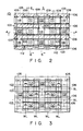
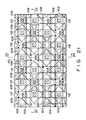
- Fig. 2 is a pattern plan view of a memory cell area of a DRAM according to a first embodiment of this invention
- Fig. 3 is a view showing the arrangement of transistors in the above pattern
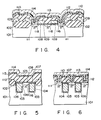
- Fig. 4 is a cross sectional view taken along the line 4-4 of Fig. 2
- Fig. 5 is a cross sectional view taken along the line 5-5 of Fig. 2
- Fig. 6 is a cross sectional view taken along the line 6-6 of Fig. 2
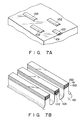
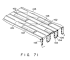
- Figs. 7A to 7F are perspective views showing a method of manufacturing the DRAM.
- the DRAM according to the first embodiment and the method for manufacturing the same are explained.
- field oxide films 102 for element isolation are formed at a regular interval on a P-type semiconductor substrate 101 by local oxidation of silicon, for example (refer to Fig. 7A).
- thermal oxide film 150 is formed by thermal oxidating the surface of the substrate 101.
- a silicon nitride film 151 and a silicon oxide film 152 are sequentially formed on the substrate 101 by use of a CVD method, for example.
- the silicon oxide film 152 the nitride film 151 and thermal oxide film 150 are sequentially etched by photo engraving technique.
- the substrate 101 is sequentially etched with the patterned the silicon oxide film 152 the nitride film 151 and thermal oxide film 150 used as a mask so as to form grooves 103 in the substrate 101 (refer to Fig. 7B).
- thermal oxide films 104 having a film thickness of approx. 500 ⁇ , for example, are formed on the exposed surfaces of the grooves 103 by thermal oxidation.
- a photoresist is used as a mask to selectively etch the thermal oxide films 104 on the exposed surfaces of the grooves 103 so as to form openings 105 therein.
- arsenic ion is implanted in an oblique direction into the semiconductor substrate 101 via the openings 105 to approx. 1 x 1015 cm ⁇ 2 (dose) so as to form n-type diffused layers 101a (refer to Figs. 2 and 5).
- a conductive film for example, phosphorus doped polysilicon is deposited on the entire surface of the semiconductor substrate 101 and is etched back by RIE, for example, to fill the grooves 103 and form bit lines 106. At this time, the openings 105 are also filled with the bit lines 106.
- bit lines 106 is thermally oxidized with the nitride film 151 used as a mask to form thermal oxide films 107.
- the bit lines 106 may be connected to the n-type diffused layer 101a (refer to Fig. 7C).
- the nitride film 151 and thermal oxide film 150 are sequentially and selectively etched out to expose the surface of the substrate 101 (refer to Fig. 7D).
- gate oxide films 108 of approx. 100 ⁇ are formed on respective element regions each of which is surrounded by adjacent two of the field oxide films 102, 102 and a corresponding one of the grooves 103 by thermal oxidation.
- a conductive film for example, phosphorus doped polysilicon is deposited to a thickness of approx. 2000 ⁇ and is patterned to form gate electrodes 109 of the transfer transistors (Fig. 7E) by photo engraving technique.
- n-type diffused layers 116 serving as the source and drain of each transistor (refer to Figs. 4 to 7F).
- an insulation film for example, oxide film 110 is formed on the resultant structure by use of the CVD method and then contact holes 111 are formed by RIE, for example, on the n-type diffused layers 116 which lie outside the gate electrode 109 by RIE by photo engraving technique (refer to Figs. 4 to 6).
- a conductive film for example, phosphorus doped polysilicon is deposited on the oxide films 110 and in the contact holes 111 and is then patterned to form storage node electrodes 112 (Fig. 7F).
- a laminated film 113 of SiO2, SiNx and SiO2 is formed as a capacitor dielectric film on the storage node electrodes 112 and the like to a thickness equivalent to a thickness of approx. 50 ⁇ of an SiO2 film and then, for example, phosphorus doped polysilicon is deposited as plate electrodes 114 (refer to Figs. 4 and 6). After this, an insulation film (not shown) is formed on the plate electrodes 114. Then, contact holes are formed in the above insulation film by photo engraving technique and A1 wirings which are connected to the gate electrodes 109, for example, are formed to complete the semiconductor device.
- the bit lines 106 are formed before the transistor and capacitors are formed, contacts between the bit lines and the n-type diffused layers of the transistors can be easily formed. Further, the contacts can be made simply by selectively removing part of the thermal oxide film 104 formed on the internal surface of the groove 103. Therefore, it is not necessary to form contact holes like the deep contact holes 512 of the conventional memory cell shown in Fig. 1. Since the bit lines are buried in the semiconductor substrate 101, the memory cell area can be made flat on substantially the entire surface. As a result, the possibility of breakage of wires at the stepped portions in the semiconductor device becomes small, and therefore a semiconductor structure suitable for high integration can be obtained.
- Formation of the grooves 103 and oxide films on the bit lines 106 can be effected according to the following method.
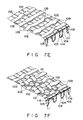
- Figs. 7G to 7I are perspective views of semiconductor structures for illustrating a method for manufacturing the DRAM memory cell according to a modification of the first embodiment.
- the field oxide films 102 are formed.
- a photoresist is formed and a pattern of the grooves 103 is formed in the photoresist by a photo etching process.
- the patterned photoresist is used as a mask to selectively etch out the semiconductor substrate 101 so as to form the grooves 103.
- the photoresist is removed.
- the exposed silicon surfaces such as the internal surfaces of the grooves 103 are thermally oxidized to form thermal oxide films 104A and 104B.
- a photoresist is again formed and a pattern of the openings 105 is formed in the photoresist by a photo etching process.
- the patterned photoresist is used as a mask to selectively etch out the oxide films 104B formed on the internal surfaces of the grooves 103 so as to form the openings 105 (Fig. 7G).
- a conductive film for example, phosphorus doped polysilicon is deposited on the entire surface of the resultant structure and the polysilicon is etched back by RIE to leave the polysilicon only in the grooves 103.
- the bit lines 106 are formed.
- the exposed top surfaces of the bit lines 106 are thermally oxidized to form thermal oxide films 107 which are thicker than the thermal oxide films 104A (Fig. 7H).
- the thermal oxide films 104A and 107 are etched. Since, at this time, the oxide film 104A is thinner than the thermal oxide film 107, the thermal oxide film 104A is completely etched out to expose part of the surface of the semiconductor substrate 101. On the other hand, the thermal oxide film 107 is not completely etched out and partly left behind on the surface of the bit lines 106.
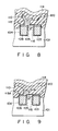
- Fig. 8 is a cross sectional view of the same portion as that of Fig. 5 and shows a DRAM according to a second embodiment of this invention.
- Fig. 8 portions which are the same as those of Figs. 2 to 6 are denoted by the same reference numerals and only different portions are explained.
- bit lines 106 and the n-type diffused layers 116 of one of the transistors are connected together via the openings 105 formed in the grooves 103, but in this embodiment, they are connected together without forming the openings 105 in the grooves 103.
- the bit lines 106 and the n-type diffused layer 116 of one of the transistors are connected together via a phosphorus doped polysilicon layer 115 formed over the oxide film 104, for example.
- a capacitor since there is a possibility that a capacitor may be formed between the phosphorus doped polysilicon layer 115 and the plate electrode 114, it is preferable to form an insulation film 120 having a sufficiently large film thickness formed on polysilicon layer 115. The capacitance between the polysilicon layer 115 and the plate electrode 114 can be reduced by forming the insulation film 120, thereby making it possible to prevent a capacitor from being formed between them.
- Fig. 9 is a cross sectional view of the same portion as that of Fig. 5 and shows a modification of the second embodiment.
- a polysilicon layer 115A which is formed in the opening by the selective epitaxial growth is used instead of the polysilicon layer 115.
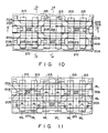
- Fig. 10 is a pattern plan view of a memory cell area of a DRAM according to a third embodiment of this invention
- Fig. 11 is a view showing the arrangement of transistors in this pattern
- Fig. 12 is a cross sectional view taken along the line 12-12 of Fig. 10
- Fig. 13 is a cross sectional view taken along the line 13-13 of Fig. 10
- Fig. 14 is a cross sectional view taken along the line 14-14 of Fig. 10.
- bit lines are formed in the semiconductor substrate, but in this embodiment, capacitors are formed in the semiconductor substrate in addition to the bit lines.
- field oxide films 202 for element isolation are formed at a regular interval on the surface of a P-type semiconductor substrate 201 (refer to Figs. 10, 12 and 14).
- thermal oxide films 204 having a film thickness of approx. 500 ⁇ , for example, are formed on the internal surfaces of the grooves 203 by thermal oxidation (refer to Figs. 10, 13 and 14).
- openings 205 are formed by partly etching the respective thermal oxide films 204 on the internal surfaces of the grooves 203 with a photoresist used as a mask. Then, ion is implanted via the openings 205 in an oblique direction to ion-implant arsenic to approx. 1 x 1015 cm ⁇ 2 (dose), for example, into portions of the semiconductor substrate 201 exposed to the openings 205 so as to form n-type diffused layers 201a (refer to Fig. 14).
- a conductive film for example, phosphorus doped polysilicon is deposited on the entire surface of the semiconductor substrate 201 and is etched back by RIE, for example, to fill the grooves 203, thus forming bit lines 206 (refer to Figs. 10, 13 and 14). At this time, the openings 205 are filled with the bit lines 206.
- oxide films 207 are formed on the exposed top surfaces of the bit lines 206 by thermal oxidation.
- the bit lines 206 are connected to the respective n-type diffused layers 201a (refer to Figs. 13 and 14).
- trenchs 208 of approx. 10 ⁇ m are formed in element regions and field oxide 202 each of which is surrounded by the adjacent field oxide films 202 and a corresponding one of the grooves 203 by RIE with a photoresist used as a mask and then arsenic ion, for example, is implanted therein to approx. 1 x 1015 cm ⁇ 2 (dose) to form n-type diffused layers (storage rode electrodes) 208a on the internal surfaces of the trenchs 208 (refer to Figs. 10, 12 and 13).
- gate oxide films 212 of approx. 100 ⁇ are formed on element regions each of which is surrounded by the grooves 203 and the plate electrode 210, and then a conductive film, for example, phosphorus doped polysilicon is deposited to approx. 2000 ⁇ and is patterned to form gate electrodes 213 of transfer transistors.
- n-type diffused layers 214 serving as the source and drain regions of the transistors are formed by implanting arsenic ion, for example, into the semiconductor substrate 201 to approx. 1 x 1015 cm ⁇ 2 (dose) (refer to Figs. 10, 12 to 14).
- an enterlevel insulator (not shown) is formed on the entire surface of the resultant structure. Then, contact holes are formed in the above interlevel insulator with a photoresist used as mask, and then Al wirings which are connected to word lines (gate electrodes 213), for example, are formed to complete the semiconductor device.
- bit lines are formed in the semiconductor substrate in the third embodiment, a contact between the bit line and one of the n-type diffused layers 214 of the transistor may be easily formed. Further, since the cell area may be made flat, the high integration density may be easily attained.
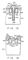
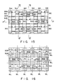
- Fig. 15 is a pattern plan view of a memory cell area of a DRAM according to a fourth embodiment of this invention
- Fig. 16 is a view showing the arrangement of transistors in the pattern
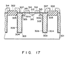
- Fig. 17 is a cross sectional view taken along the line 17-17 of Fig.
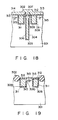
- Fig. 18 is a cross sectional view taken along the line 18-18 of Fig.
- Fig. 19 is a cross sectional view taken along the line 19-19 of Fig. 15.
- bit lines 206 and the n-type diffused layers (storage node electrodes) 208a, laminated films 208 and plate electrodes 210 which constitute capacitors are formed in the semiconductor substrate, but in this embodiment, bit lines are buried in the semiconductor substrate and the semiconductor substrate is used as a plate electrode of the capacitor.
- field oxide films 302 are formed on the surface of a P-type semiconductor substrate 301 with a preset distance set therebetween (refer to Figs. 15, 17 to 19).
- trenchs 303 of approx. 10 ⁇ m are formed in desired portions of the element regions and field oxide films 302 by RIE and oxide films 304 of approx. 100 ⁇ used as capacitor dielectric films are formed on the internal side surfaces of the trenchs 303 by thermal oxidation (refer to Figs. 15, 17 and 18).
- portion of the oxide film 304 is selectively etched with a photoresist used as a mask to form openings 305.
- the photoresist is removed and ion is implanted via the openings 205 in an oblique direction to ion-implant arsenic to approx. 1 x 1015 cm ⁇ 2 (dose), for example, into those portions of the semiconductor substrate 301 which are exposed to the openings 305 so as to form n-type diffused layers 301a.
- a conductive film for example, phosphorus doped polysilicon is deposited in the trenchs 303 and etched back by RIE, for example, to form storage node electrodes 306 (Figs. 17 and 18).
- thermal oxide films 307 are formed on the exposed top exposed surfaces of the storage node electrodes 306 by thermal oxidation.
- the storage node electrodes 306 are connected to the respective n-type diffused layers 301a via the openings 305 (refer to Fig. 17).
- grooves 308 are formed with a preset distance set there between in the semiconductor substrate 301 and then thermal oxide films 309 of approx. 500 ⁇ are formed on the internal surfaces of the grooves 308 by thermal oxidation (refer to Figs. 15, 18 and 19).
- portions of the thermal oxide films 309 are etched with a photoresist used as a mask to form openings 310.
- ion is implanted via the openings 310 in an oblique direction to ion-implant arsenic to approx. 1 x 1015 cm ⁇ 2 (dose), for example, into those portions of the semiconductor substrate 301 which are exposed to the openings 310 so as to form n-type diffused layers 301b (refer to Figs. 15 and 19).
- a conductive film for example, phosphorus doped polysilicon is deposited on the entire surface of the semiconductor substrate 301 and then etched back to fill the grooves 308 by RIE, for example, so as to form bit lines 311 (refer to Figs. 15, 18 and 19).
- thermal oxide films 312 are formed on the top exposed surface of the bit lines 311 by thermal oxidation. At this time, the bit lines 311 are connected to the n-type diffused layers 301b via the openings 310 (refer to Fig. 19).
- gate oxide films 313 of 100 ⁇ are formed on element regions surrounded by the field oxide film 302 and grooves 308 by thermal oxidation and a conductive film, for example, phosphorus doped polysilicon is deposited to approx. 2000 ⁇ on the resultant structure and is patterned to form gate electrodes 314 of the transfer transistors.
- arsenic ion is implanted to approx. 1 x 1015 cm ⁇ 2 (dose) for example, into the substrate 301 to form n-type diffused layers 315 serving as the source and drain regions of the transistors (Figs. 17 and 19).
- an interlevel insulator (not shown) is formed and contact holes are formed in the interlevel insulator with a photoresist used as a mask, and then A1 wirings which are electrically connected to the gate electrodes 314, for example, and the like are formed to complete the semiconductor device.
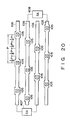
- Fig. 20 is a view showing a pattern in which the positions of contacts between the bit lines and the drain regions of the transfer transistors are deviated by 1/2n (n is an integer) pitch
- Fig. 21 is a pattern plan view of a memory cell area of a DRAM according to a fifth embodiment of this invention
- Fig. 22 is a view showing the arrangement of transistors in the pattern
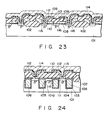
- Fig. 23 is a cross sectional view taken along the line 23-23 of Fig. 21
- Fig. 24 is a cross sectional view taken along the line 24-24 of Fig. 21.
- This embodiment is different from the first embodiment in the arrangement of the memory cells of the DRAM and the construction of the cell is the same as that shown in Figs. 2 to 6.
- Figs. 20 to 24 portions which are the same as those of Figs. 2 to 6 are denoted by the same reference numerals.
- a pattern in which the positions of contacts between the bit lines and the drain regions of the transfer transistors are deviated by 1/2n (n is an integer) pitch is used.
- the pattern is schematically shown in Fig. 20.
- bit line sense amplifiers 407 and 408 are connected to the opposite ends of a plurality of bit lines 106 which are arranged in parallel. More specifically, two bit lines lying on both sides of an odd-numbered or even-numbered bit line and making a complementary pair are connected at one or the other end thereof to one of the sense amplifiers 407 and 408.
- Each of the bit lines 106 has contacts 105 for the drains (or sources) of the transfer transistors arranged at a constant pitch in the lengthwise direction thereof. In this case, the contact position of one of the bit lines are deviated from the contact position of the adjacent bit line by 1/4 pitch in the lengthwise direction of the bit line.
- Figs. 20 to 24 show the arrangement of the memory cells explained in the first embodiment in the above pattern.
- bit lines and word lines are arranged in directions to intersect each other and an element region for two transfer transistors are formed as to cross two bit lines and two adjacent word lines. Further, each of the bit lines are connected to capacitors corresponding to two transfer transistors at portions which intersect the element regions at a constant pitch P in the lengthwise direction thereof so as to form two cells of one-transistor/one-capacitor structure in each element region.
- the position of contact of each of the bit lines are deviated from the position of contact of the adjacent bit line by substantially 1/4 pitch in the lengthwise direction of the bit line.
- a semiconductor memory device and a method for manufacturing the same in which since the cell structure can be made flat by burying the bit lines in the internal portion of the semiconductor substrate, bit line contacts may be easily obtained in comparison with the prior art case.
Landscapes
- Engineering & Computer Science (AREA)
- Manufacturing & Machinery (AREA)
- Semiconductor Memories (AREA)
- Internal Circuitry In Semiconductor Integrated Circuit Devices (AREA)
Applications Claiming Priority (2)
| Application Number | Priority Date | Filing Date | Title |
|---|---|---|---|
| JP42431/90 | 1990-02-26 | ||
| JP2042431A JPH0821689B2 (ja) | 1990-02-26 | 1990-02-26 | 半導体記憶装置およびその製造方法 |
Publications (2)
| Publication Number | Publication Date |
|---|---|
| EP0444615A1 true EP0444615A1 (de) | 1991-09-04 |
| EP0444615B1 EP0444615B1 (de) | 1996-04-17 |
Family
ID=12635880
Family Applications (1)
| Application Number | Title | Priority Date | Filing Date |
|---|---|---|---|
| EP91102827A Expired - Lifetime EP0444615B1 (de) | 1990-02-26 | 1991-02-26 | Dynamische Speicheranordnung mit wahlfreiem Zugriff mit Bitleitungen, die im Substrat vergraben sind |
Country Status (5)
| Country | Link |
|---|---|
| US (1) | US5410169A (de) |
| EP (1) | EP0444615B1 (de) |
| JP (1) | JPH0821689B2 (de) |
| KR (1) | KR940005886B1 (de) |
| DE (1) | DE69118737T2 (de) |
Cited By (1)
| Publication number | Priority date | Publication date | Assignee | Title |
|---|---|---|---|---|
| WO2001099152A3 (en) * | 2000-06-21 | 2002-04-04 | Infineon Technologies Corp | Buried bit line-field plate isolation defined dram cell active areas |
Families Citing this family (38)
| Publication number | Priority date | Publication date | Assignee | Title |
|---|---|---|---|---|
| JP2795156B2 (ja) * | 1993-12-28 | 1998-09-10 | 日本電気株式会社 | 半導体集積回路装置の製造方法及び半導体集積回路装置 |
| US5492853A (en) * | 1994-03-11 | 1996-02-20 | Micron Semiconductor, Inc. | Method of forming a contact using a trench and an insulation layer during the formation of a semiconductor device |
| US5497017A (en) * | 1995-01-26 | 1996-03-05 | Micron Technology, Inc. | Dynamic random access memory array having a cross-point layout, tungsten digit lines buried in the substrate, and vertical access transistors |
| JPH09219500A (ja) * | 1996-02-07 | 1997-08-19 | Taiwan Moshii Denshi Kofun Yugenkoshi | 高密度メモリ構造及びその製造方法 |
| US5684314A (en) * | 1996-03-18 | 1997-11-04 | Kenney; Donald M. | Trench capacitor precharge structure and leakage shield |
| US5854128A (en) * | 1996-04-29 | 1998-12-29 | Micron Technology, Inc. | Method for reducing capacitive coupling between conductive lines |
| US5909618A (en) * | 1997-07-08 | 1999-06-01 | Micron Technology, Inc. | Method of making memory cell with vertical transistor and buried word and body lines |
| US6191470B1 (en) | 1997-07-08 | 2001-02-20 | Micron Technology, Inc. | Semiconductor-on-insulator memory cell with buried word and body lines |
| US6072209A (en) | 1997-07-08 | 2000-06-06 | Micro Technology, Inc. | Four F2 folded bit line DRAM cell structure having buried bit and word lines |
| US5973356A (en) * | 1997-07-08 | 1999-10-26 | Micron Technology, Inc. | Ultra high density flash memory |
| US5936274A (en) * | 1997-07-08 | 1999-08-10 | Micron Technology, Inc. | High density flash memory |
| US6150687A (en) | 1997-07-08 | 2000-11-21 | Micron Technology, Inc. | Memory cell having a vertical transistor with buried source/drain and dual gates |
| US5914511A (en) * | 1997-10-06 | 1999-06-22 | Micron Technology, Inc. | Circuit and method for a folded bit line memory using trench plate capacitor cells with body bias contacts |
| US5907170A (en) * | 1997-10-06 | 1999-05-25 | Micron Technology, Inc. | Circuit and method for an open bit line memory cell with a vertical transistor and trench plate trench capacitor |
| US6528837B2 (en) | 1997-10-06 | 2003-03-04 | Micron Technology, Inc. | Circuit and method for an open bit line memory cell with a vertical transistor and trench plate trench capacitor |
| US6066869A (en) * | 1997-10-06 | 2000-05-23 | Micron Technology, Inc. | Circuit and method for a folded bit line memory cell with vertical transistor and trench capacitor |
| DE59814170D1 (de) * | 1997-12-17 | 2008-04-03 | Qimonda Ag | Speicherzellenanordnung und Verfahren zu deren Herstellung |
| US6025225A (en) * | 1998-01-22 | 2000-02-15 | Micron Technology, Inc. | Circuits with a trench capacitor having micro-roughened semiconductor surfaces and methods for forming the same |
| US6246083B1 (en) * | 1998-02-24 | 2001-06-12 | Micron Technology, Inc. | Vertical gain cell and array for a dynamic random access memory |
| US6242775B1 (en) | 1998-02-24 | 2001-06-05 | Micron Technology, Inc. | Circuits and methods using vertical complementary transistors |
| US5963469A (en) * | 1998-02-24 | 1999-10-05 | Micron Technology, Inc. | Vertical bipolar read access for low voltage memory cell |
| US6304483B1 (en) | 1998-02-24 | 2001-10-16 | Micron Technology, Inc. | Circuits and methods for a static random access memory using vertical transistors |
| US6124729A (en) * | 1998-02-27 | 2000-09-26 | Micron Technology, Inc. | Field programmable logic arrays with vertical transistors |
| US5991225A (en) * | 1998-02-27 | 1999-11-23 | Micron Technology, Inc. | Programmable memory address decode array with vertical transistors |
| US6043527A (en) * | 1998-04-14 | 2000-03-28 | Micron Technology, Inc. | Circuits and methods for a memory cell with a trench plate trench capacitor and a vertical bipolar read device |
| US6025261A (en) | 1998-04-29 | 2000-02-15 | Micron Technology, Inc. | Method for making high-Q inductive elements |
| US6696746B1 (en) | 1998-04-29 | 2004-02-24 | Micron Technology, Inc. | Buried conductors |
| US6093623A (en) | 1998-08-04 | 2000-07-25 | Micron Technology, Inc. | Methods for making silicon-on-insulator structures |
| US6134175A (en) | 1998-08-04 | 2000-10-17 | Micron Technology, Inc. | Memory address decode array with vertical transistors |
| US6208164B1 (en) | 1998-08-04 | 2001-03-27 | Micron Technology, Inc. | Programmable logic array with vertical transistors |
| US6423613B1 (en) | 1998-11-10 | 2002-07-23 | Micron Technology, Inc. | Low temperature silicon wafer bond process with bulk material bond strength |
| DE19911149C1 (de) * | 1999-03-12 | 2000-05-18 | Siemens Ag | Integrierte Schaltungsanordnung, die eine in einem Substrat vergrabene leitende Struktur umfaßt, die mit einem Gebiet des Substrats elektrisch verbunden ist, und Verfahren zu deren Herstellung |
| WO2000077848A1 (en) * | 1999-06-10 | 2000-12-21 | Infineon Technologies North America Corp. | Self-aligned buried strap for vertical transistors in semiconductor memories |
| US6852167B2 (en) | 2001-03-01 | 2005-02-08 | Micron Technology, Inc. | Methods, systems, and apparatus for uniform chemical-vapor depositions |
| US6624515B1 (en) | 2002-03-11 | 2003-09-23 | Micron Technology, Inc. | Microelectronic die including low RC under-layer interconnects |
| US7589029B2 (en) | 2002-05-02 | 2009-09-15 | Micron Technology, Inc. | Atomic layer deposition and conversion |
| US7160577B2 (en) | 2002-05-02 | 2007-01-09 | Micron Technology, Inc. | Methods for atomic-layer deposition of aluminum oxides in integrated circuits |
| US7927948B2 (en) | 2005-07-20 | 2011-04-19 | Micron Technology, Inc. | Devices with nanocrystals and methods of formation |
Citations (1)
| Publication number | Priority date | Publication date | Assignee | Title |
|---|---|---|---|---|
| US4912535A (en) * | 1987-08-08 | 1990-03-27 | Mitsubishi Denki Kabushiki Kaisha | Trench type semiconductor memory device having side wall contact |
Family Cites Families (10)
| Publication number | Priority date | Publication date | Assignee | Title |
|---|---|---|---|---|
| US4811067A (en) * | 1986-05-02 | 1989-03-07 | International Business Machines Corporation | High density vertically structured memory |
| JPS63158868A (ja) * | 1986-12-23 | 1988-07-01 | Oki Electric Ind Co Ltd | 半導体メモリ装置 |
| JPS63263758A (ja) * | 1987-04-22 | 1988-10-31 | Hitachi Ltd | 半導体メモリ |
| JPS63300550A (ja) * | 1987-05-29 | 1988-12-07 | Nec Corp | 半導体記憶装置 |
| JPS6411360A (en) * | 1987-07-06 | 1989-01-13 | Hitachi Ltd | Semiconductor memory device |
| JPH0824167B2 (ja) * | 1987-12-02 | 1996-03-06 | 三菱電機株式会社 | 半導体記憶装置 |
| JPS6442167A (en) * | 1987-08-08 | 1989-02-14 | Mitsubishi Electric Corp | Semiconductor memory device |
| JP2530175B2 (ja) * | 1987-09-09 | 1996-09-04 | 富士通株式会社 | 半導体記憶装置の製造方法 |
| JPH01160047A (ja) * | 1987-12-16 | 1989-06-22 | Fujitsu Ltd | 半導体記憶装置とその製造方法 |
| JPH01257364A (ja) * | 1988-04-07 | 1989-10-13 | Hitachi Ltd | 半導体装置の製造方法 |
-
1990
- 1990-02-26 JP JP2042431A patent/JPH0821689B2/ja not_active Expired - Fee Related
-
1991
- 1991-02-22 KR KR1019910002889A patent/KR940005886B1/ko not_active Expired - Fee Related
- 1991-02-26 DE DE69118737T patent/DE69118737T2/de not_active Expired - Fee Related
- 1991-02-26 EP EP91102827A patent/EP0444615B1/de not_active Expired - Lifetime
-
1993
- 1993-02-22 US US08/020,444 patent/US5410169A/en not_active Expired - Lifetime
Patent Citations (1)
| Publication number | Priority date | Publication date | Assignee | Title |
|---|---|---|---|---|
| US4912535A (en) * | 1987-08-08 | 1990-03-27 | Mitsubishi Denki Kabushiki Kaisha | Trench type semiconductor memory device having side wall contact |
Non-Patent Citations (5)
| Title |
|---|
| PATENT ABSTRACTS OF JAPAN, vol. 13, no. 136 (E-737)[3484], 5th April 1989; & JP-A-63 300 550 (NEC CORP.) 07-12-1988 * |
| PATENT ABSTRACTS OF JAPAN, vol. 13, no. 186 (E-752)[3534], 2nd May 1989; & JP-A-1 011 360 (HITACHI LTD) 13-01-1989 * |
| PATENT ABSTRACTS OF JAPAN, vol. 13, no. 280 (E-779)[3628], 27th June 1989; & JP-A-1 067 956 (FUJITSU LTD) 14-03-1989 * |
| PATENT ABSTRACTS OF JAPAN, vol. 13, no. 429 (E-823)[3777], 25th September 1989; & JP-A-1 160 047 (FUJITSU LTD) 22-06-1989 * |
| PATENT ABSTRACTS OF JAPAN, vol. 13, no. 86 (E-720)[3434], 28th February 1989; & JP-A-63 263 758 (HITACHI LTD) 31-10-1988 * |
Cited By (1)
| Publication number | Priority date | Publication date | Assignee | Title |
|---|---|---|---|---|
| WO2001099152A3 (en) * | 2000-06-21 | 2002-04-04 | Infineon Technologies Corp | Buried bit line-field plate isolation defined dram cell active areas |
Also Published As
| Publication number | Publication date |
|---|---|
| JPH03246966A (ja) | 1991-11-05 |
| US5410169A (en) | 1995-04-25 |
| DE69118737T2 (de) | 1996-09-26 |
| DE69118737D1 (de) | 1996-05-23 |
| JPH0821689B2 (ja) | 1996-03-04 |
| EP0444615B1 (de) | 1996-04-17 |
| KR940005886B1 (ko) | 1994-06-24 |
| KR920000142A (ko) | 1992-01-10 |
Similar Documents
| Publication | Publication Date | Title |
|---|---|---|
| EP0444615B1 (de) | Dynamische Speicheranordnung mit wahlfreiem Zugriff mit Bitleitungen, die im Substrat vergraben sind | |
| US5753526A (en) | Manufacturing process of a semiconductor memory device including a trench capacitor and a surrounding gate transistor | |
| US5798544A (en) | Semiconductor memory device having trench isolation regions and bit lines formed thereover | |
| US4920065A (en) | Method of making ultra dense dram cells | |
| KR950009890B1 (ko) | 반도체기억장치 | |
| US5504027A (en) | Method for fabricating semiconductor memory devices | |
| KR100509210B1 (ko) | Dram셀장치및그의제조방법 | |
| GB2288276A (en) | Dram memory cell utilising surrounding gate transistor and method of manufacture | |
| US5523542A (en) | Method for making dynamic random access memory cell capacitor | |
| KR100325472B1 (ko) | 디램 메모리 셀의 제조 방법 | |
| US4737829A (en) | Dynamic random access memory device having a plurality of one-transistor type memory cells | |
| EP0398249B1 (de) | Halbleiterspeichervorrichtung | |
| KR930001221B1 (ko) | 다이나믹 반도체 메모리의 3차원적 i-트랜지스터 셀 장치 및 그 제조방법 | |
| KR100251217B1 (ko) | 동적 램과 그의 제조 공정 | |
| US7214572B2 (en) | Semiconductor memory device and manufacturing method thereof | |
| KR0151197B1 (ko) | 반도체 메모리장치 및 그 제조방법 | |
| US5488242A (en) | Semiconductor memory device | |
| KR950012034B1 (ko) | 반도체 기억장치의 제조방법 | |
| KR910002039B1 (ko) | 반도체기억장치의 제조방법 | |
| KR100325471B1 (ko) | 디램의 제조 방법 | |
| EP0457131A1 (de) | Methode zur Herstellung eines Halbleiterspeicherbauteils mit Stapelkondensatorzellen | |
| US5065215A (en) | Semiconductor memory cell and method of manufacturing the same | |
| US5248891A (en) | High integration semiconductor device | |
| JPH08274275A (ja) | 半導体装置およびその製造方法 | |
| KR100316577B1 (ko) | 반도체 메모리 셀 |
Legal Events
| Date | Code | Title | Description |
|---|---|---|---|
| PUAI | Public reference made under article 153(3) epc to a published international application that has entered the european phase |
Free format text: ORIGINAL CODE: 0009012 |
|
| 17P | Request for examination filed |
Effective date: 19910226 |
|
| AK | Designated contracting states |
Kind code of ref document: A1 Designated state(s): DE FR GB |
|
| 17Q | First examination report despatched |
Effective date: 19940426 |
|
| GRAA | (expected) grant |
Free format text: ORIGINAL CODE: 0009210 |
|
| AK | Designated contracting states |
Kind code of ref document: B1 Designated state(s): DE FR GB |
|
| REF | Corresponds to: |
Ref document number: 69118737 Country of ref document: DE Date of ref document: 19960523 |
|
| ET | Fr: translation filed | ||
| PLBE | No opposition filed within time limit |
Free format text: ORIGINAL CODE: 0009261 |
|
| STAA | Information on the status of an ep patent application or granted ep patent |
Free format text: STATUS: NO OPPOSITION FILED WITHIN TIME LIMIT |
|
| 26N | No opposition filed | ||
| REG | Reference to a national code |
Ref country code: GB Ref legal event code: 746 Effective date: 19981007 |
|
| REG | Reference to a national code |
Ref country code: FR Ref legal event code: D6 |
|
| REG | Reference to a national code |
Ref country code: GB Ref legal event code: IF02 |
|
| PGFP | Annual fee paid to national office [announced via postgrant information from national office to epo] |
Ref country code: FR Payment date: 20030210 Year of fee payment: 13 |
|
| PGFP | Annual fee paid to national office [announced via postgrant information from national office to epo] |
Ref country code: GB Payment date: 20030226 Year of fee payment: 13 |
|
| PG25 | Lapsed in a contracting state [announced via postgrant information from national office to epo] |
Ref country code: GB Free format text: LAPSE BECAUSE OF NON-PAYMENT OF DUE FEES Effective date: 20040226 |
|
| GBPC | Gb: european patent ceased through non-payment of renewal fee |
Effective date: 20040226 |
|
| PG25 | Lapsed in a contracting state [announced via postgrant information from national office to epo] |
Ref country code: FR Free format text: LAPSE BECAUSE OF NON-PAYMENT OF DUE FEES Effective date: 20041029 |
|
| REG | Reference to a national code |
Ref country code: FR Ref legal event code: ST |
|
| PGFP | Annual fee paid to national office [announced via postgrant information from national office to epo] |
Ref country code: DE Payment date: 20070222 Year of fee payment: 17 |
|
| PG25 | Lapsed in a contracting state [announced via postgrant information from national office to epo] |
Ref country code: DE Free format text: LAPSE BECAUSE OF NON-PAYMENT OF DUE FEES Effective date: 20080902 |