EP0443989B1 - Abfühlschaltung zum Lesen von in nichtflüchtigen Speicherzellen gespeicherten Daten - Google Patents
Abfühlschaltung zum Lesen von in nichtflüchtigen Speicherzellen gespeicherten Daten Download PDFInfo
- Publication number
- EP0443989B1 EP0443989B1 EP91830036A EP91830036A EP0443989B1 EP 0443989 B1 EP0443989 B1 EP 0443989B1 EP 91830036 A EP91830036 A EP 91830036A EP 91830036 A EP91830036 A EP 91830036A EP 0443989 B1 EP0443989 B1 EP 0443989B1
- Authority
- EP
- European Patent Office
- Prior art keywords
- current
- cell
- condition
- circuit
- branch
- Prior art date
- Legal status (The legal status is an assumption and is not a legal conclusion. Google has not performed a legal analysis and makes no representation as to the accuracy of the status listed.)
- Expired - Lifetime
Links
- 230000015654 memory Effects 0.000 title claims description 26
- 230000006399 behavior Effects 0.000 claims description 3
- 238000010586 diagram Methods 0.000 description 19
- 230000003068 static effect Effects 0.000 description 10
- 230000001052 transient effect Effects 0.000 description 8
- 230000000694 effects Effects 0.000 description 6
- 239000011159 matrix material Substances 0.000 description 5
- 230000004044 response Effects 0.000 description 5
- XUIMIQQOPSSXEZ-UHFFFAOYSA-N Silicon Chemical compound [Si] XUIMIQQOPSSXEZ-UHFFFAOYSA-N 0.000 description 3
- 229910052710 silicon Inorganic materials 0.000 description 3
- 239000010703 silicon Substances 0.000 description 3
- 238000000034 method Methods 0.000 description 2
- 230000008569 process Effects 0.000 description 2
- 230000009467 reduction Effects 0.000 description 2
- 238000013459 approach Methods 0.000 description 1
- 238000005452 bending Methods 0.000 description 1
- 238000011156 evaluation Methods 0.000 description 1
- 230000006870 function Effects 0.000 description 1
- 230000010354 integration Effects 0.000 description 1
- 238000012856 packing Methods 0.000 description 1
- 230000003071 parasitic effect Effects 0.000 description 1
- 238000012552 review Methods 0.000 description 1
- 239000004065 semiconductor Substances 0.000 description 1
Images

Classifications
-
- G—PHYSICS
- G11—INFORMATION STORAGE
- G11C—STATIC STORES
- G11C16/00—Erasable programmable read-only memories
- G11C16/02—Erasable programmable read-only memories electrically programmable
- G11C16/06—Auxiliary circuits, e.g. for writing into memory
- G11C16/26—Sensing or reading circuits; Data output circuits
- G11C16/28—Sensing or reading circuits; Data output circuits using differential sensing or reference cells, e.g. dummy cells
Definitions
- the present invention relates to a circuit for reading the information stored in ROM and EPROM type memories accordding to a differential sensing mode and, in particular to an improved circuit for generating an offsetting current for discrimimating between the currents which flow through a certain cell of the memory array which has been selectively addressed for reading and a virgin reference cell, according to a current offset sensing mode.
- EPROM memories represent one of the most advanced field of integration in silicon.
- semiconductor nonvolatile memories EPROM memories represent one of the most advanced field of integration in silicon.
- new devices with a capacity of up to 4 megabit have been presented nowadays and new ambitious goals are announced.
- the memory market requires improved performances in terms of access time, write time and power consumption.
- the reduction of the size of the devices poses serious problems to the achievement of these aims.
- the access time during a reading phase is penalized by a consequent reduction of the actual current through the memory cell and an increased influence of parasitic electric factors of the integrated structure of the cells.
- the circuits used for reading the information stored in the cells must possess an enhanced precision and reliability.
- a differential type sense circuit Basically, the architecture of a differential type sense circuit are by far more precise and less sensitive to the effects of "process spread", temperature and supply voltage variations, by treating them essentially as common mode contributions.
- a load-offset type and a current-offset type.
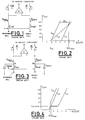
- a load-offset (or load-unbalance) type sense circuit and the relative operating characteristics are reproduced in Figures 1 and 2, respectively.
- the reading system is based, as it is well known, upon the unbalancing of the load transistors, respectively of the "array cell” side and of the "reference cell” side (where the reference cell is commonly constituted by a virgin memory cell), by making larger than unity the dimensional ratio between the two load transistors.
- the unbalancing of the loads permits the reading of a virgin cell by introducing an element of asymmetry between the two branches of the differential sense circuit.
- the respective characteristics of a virgin cell (I on ) and of a written cell (I off ) and of the reference current (I ref ) are all shown on a single diagram purposely.
- the reference current I ref varies with the varying of the supply voltage VCC which is applied to the control gate of the reference cell.
- the minimum working voltage VCC min is in this case limited by the threshold of a virgin cell V th , while the maximum operating voltage VCC max is given by the equality between I ref and I off .
- EP-A-0 326 004-A2 discloses a sensing circuit operating in a current-offset mode, wherein a generator of an offset current is connected between the drain of the reference memory cell and the supply rail and generates and offset current which is substantially constant irrespectively of the supply voltage variations.
- FIG. 3 A typical circuit diagram and relative characteristics of a sensing system operating in a current-offset mode, are shown in Figures 3 and 4, respectively.
- the operating range in terms of voltage VCC is widened by modifying the reference current I ref characteristic.
- the load transistors have similar dimensions.
- the element of asymmetry which is necessary for discriminating the sensing of a virgin cell, is provided by means of a constant current I offset which is purposely added in parallel to the cell current of the array side.
- VCC max value tends theorethically to infinity for all the cells which have undergone a threshold shift ( ⁇ V th ) larger than the value of said additional constant current (I offset ) divided by the current gain of the cell: i.e. ⁇ V th > I offset ⁇
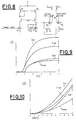
- the static characteristics discussed above define the correct margin of operation, that is of correct interpretation of the data stored in an array cell, in function of the supply voltage and therefore they offer a measure of the width of the operating range of the sense circuits toward VCC , in the hypotesis that all transients, such as the precharging of the column lines ( BITLINES ), the signal propagation along the relative row of the array and so forth have terminated.
- the dynamic characteristics have a relevance on the currents passing in the two branches of the input circuit of the differential sense amplifier during a typical reading phase, during which the actual supply voltage of the device is set, thus providing for an evaluation of the correct operation margin during a transient.
- These dynamic characteristcs are indicative of how small will be the access time of the memory, because the response of the sense circuits will be correct only from the moment in which the current of the reference side is smaller than the current of the array side when reading a conducting cell (ON-programmed cell), and viceversa, when reading a nonconducting cell (OFF-programmed cell).
- the sense circuit in the case of a load-unbalance system, the current in the two branches (reference side and array side) of the sense circuit are intrinsically different for any value of the gate voltage of the cells (and therefore the circuit provides a correct sensing during a transient), in the case of a current-offset sense circuit, because the circuit is powered at VCC, there is not a transient phase for the value of the current set by the offsetting circuit and therefore, when an OFF-programmed cell must be read, the sense circuit initially provides an erroneous response because the reference side current, for a low value of the voltage applied to the gate of the array cell and of the reference cell, is lower than the current of the array side, which current represents the sum of the offsetting current, which is intrinsically constant, and of the current of the OFF-programmed cell, which is practically nil.
- the device for generating an unbalance between a reference cell branch of the sense circuit and another branch of the circuit comprising the selectively addressed array cell to be read which is employed is basically a current generator and therefore, as in the case of a current-offset sense circuit of the prior art, the sizes of the load transistors of the array side and of the reference side of the differential sense circuit are advantageously identical, thus avoiding the above mentioned drawbacks typical of a load-unbalance sense circuit.
- the circuit is driven essentially by the same gate voltage which is present on the array cells and for this purpose it is necessary to introduce in the array of cells a supplementary row which is decoded at every reading, and which replicates during transients the behaviour of the array's row which is selected for reading.
- the label DUMMY ROW used in Figures 5 and 8 indicates a drive voltage line derived from a supplementary row of cells of the array of cells which is decoded at every reading and which therefore replicates perfectly the behaviour of anyone row of memory cells of the array which is selected for reading, during a transient.
- the reference column line, REFERENCE BITLINE serves a certain number of column lines, MATRIX BITLINE , of the array and to these is adjacently formed on the silicon chip so as to make as similar as possible the voltages present on the gate of the reference cell and on the gate of a selected cell of the array also during transients, the latter having a nonnegligeable duration because of the RC value of a row of the array.
- This topographic closeness between these lines further enhances a maximum geometrical identity of the relative reference cells and array cells.
- n1 , n3 , n4 and n5 are cells (transistors) electrically equivalent to anyone memory cell of the memory array programmed in an ON-condition.
- the circuit is provided also with two compensation transistors n2 and n6 , which are functionally unnecessary, but serve advantageously as compensating elements when the array cells, programmed in an-OFF condition (written cells) are not in a perfectly cut-off condition, but which in practice begin to conduct a certain current, in the order microampers, beyond a certain level of the driving voltage applied thereto.
- This condition is "replicated", by analogy, also by said transistors (cells) n2 and n6 , which are electrically equivalent to any other memory cell of the array programmed in an OFF-condition, thus obtaining as a result a perfect compensation of the current which may be conducted by written memory cells and which would disturb the process of unbalancing the currents which is performed by the circuit of the invention, thus introducing a certain limitation toward the maximum value of the driving voltage (VCC max ) by "bending" the current characteristic of the reference branch of the circuit toward the current characteristic of a written (OFF) cell until crossing it.
- VCC max maximum value of the driving voltage
- n1 , n2 and n6 are driven by said supplementary array row, DUMMY ROW , and are topologically near, on the silicon chip, to the reference column line: REFERENCE BITLINE and to the respective array column lines: MATRIX BITLINE .
- REFERENCE BITLINE REFERENCE BITLINE
- MATRIX BITLINE MATRIX BITLINE
- the current of the cell n1 is equal in any instant to the current flowing through any selected ON-programmed cell of the array, because these currents depend exclusively on the respective gate voltages, which are equal in both cells also during a transient.
- the current I on generated by the cell n1 which is identical to the current flowing through the selected cell of the array which must be read, is mirrored by the current mirror formed by the transistors p1 and p2 into the right hand branch of the mirror and it is divided into two identical semi-currents by means of the n-channel current mirror formed by the transistors n3 , n4 and n5 , all having the same size, and it is further delivered to the column line of the array side ( MATRIX BITLINE ).
- I offset 2 ⁇ I offset .
- the effect of unbalancing the currents of the two input branches ( MATRIX BITLINE and REFERENCE BITLINE , respectively) of the differential sense circuit so obtained is from both a static and a dynamic point of view, substantially similar to the effect obtained in a load-unbalance type, sense circuit, where the size of the load of the reference side is twice the size of the load of the array side, thus producing an operating characteristic similar to the one depicted in Fig. 2 .
- the unbalancing circuit is, on the other hand, exempt of the drawbacks of a load-unbalance circuit.
- VCC max the maximum value of the driving voltage
- the optional compensation transistors n2 and n6 which are, as already said, equivalent to a programmed array cell, i.e. have a high threshold, as a cell in an OFF-condition, and they are driven by the supplementary row DUMMY ROW , of the array as the cell n1 .
- the drain of the transistor n6 is connected to the reference column line: REFERENCE BITLINE , while the eventual current contribution of the transistor (cell) n2 , which is subtantially connected in common with the first transistor n1 , and which will essentially be identical to the current eventually carried by a written memory cell (OFF-programmed cell) of the array, will be summed with the current generated by n1 , thus producing a sum current (I on + I off ) of the currents generated by n1 and n2 , respectively.
- the current generating circuit for the sense circuit of the invention may also be realized in the form shown in the diagram of Fig. 8 .
- the diagram is similar to that of Fig. 5 , and therein the current contribution given by the cell n2 at the moment of generating the unbalancing current lacks completely.
- MATRIX BITLINE and REFERENCE BITLINE may be considered similar to the effect occurring in a load-unbalance-type sense circuit.
- the current generating circuit according to the Fig. 8 embodiment does not provide a static operation performance comparable to that of the circuit made in accordance with the Fig. 5 embodiment which, as shown before, has no limitation toward VCC by virtue of the contribution of transistors n2 and n6 .
- the circuit of Fig. 8 is nevertheless simpler to implement because the required supplementary row, DUMMY ROW , drives a single transistor instead of three transistors and therefore has a reduced capacitive load, positively reflecting upon the dynamic response of the current generating circuit.
- the dynamic characteristics of Fig. 6 and 9 it may be observed that, for the circuit of Fig. 8 , the characteristic curves of the reference current I ref and of the current I on of an ON-programmed cell, diverge more rapidly during a transient than those of the circuit of Fig. 5 .
Landscapes
- Read Only Memory (AREA)
- Static Random-Access Memory (AREA)
Claims (3)
- Speicherbauelement mit Speicherzellen vom EPROM- und/oder ROM-Typ und einer Leseschaltung zum Lesen der Speicherzellen, wobei die Speicherzellen in einen EIN-Zustand oder einen AUS-Zustand programmierbar oder programmiert sind, in einem Feld aus Spalten und Reihen von Zellen organisiert und selektiv über Reihenleitungen und Bitleitungen adressierbar sind, wobei die Leseschaltung einen Differenzverstärker (A) verwendet, um die Leitfähigkeit einer ausgewählten Feldzelle zu unterscheiden von der Leitfähigkeit einer Referenzzelle im EIN-Zustand, die Feldzelle und die Referenzzelle funktionell in Reihe an einen ersten bzw. an einen zweiten Zweig einer Eingangsschaltung des Differenzverstärkers zwischen einer Stromversorgungsschiene und Masse angeschlossen sind, die Leseschaltung außerdem eine Versetzungseinrichtung aufweist, die in der Lage ist, ein Unterscheidungs-Ungleichgewicht zwischen den Stärken der durch die zwei Zweige der Eingangsschaltung des Differenzverstärkers zwischen der Versorgungsspannungsschiene und Masse fließenden Ströme zu veranlassen, wobei die Versetzungseinrichtung eine Versetzungs-Stromgeneratorschaltung ist, die durch mindestens einen ersten Transistor (n1) gebildet wird, durch den ein erster Strom fließt, und dessen elektrische Kennwerte zu den elektrischen Kennwerten irgendeiner Zelle der in einen EIN-Zustand programmierten Speicherzelle äquivalent ist, und einen ersten Stromspiegel aufweist, um den ersten Strom (Ion) in einem Ausgangszweig des ersten Stromspiegels zu spiegeln, dadurch gekennzeichnet, daßder erste Transistor ein Gate aufweist, an welches eine Treiberspannung angelegt wird, die im wesentlichen identisch ist mit der an ein Gate einer zum Lesen ausgewählten Feldzelle angelegten Spannung, um den ersten Strom (Ion) zu erzeugen, der im wesentlichen identisch ist mit dem durch eine ausgewählte Feldzelle fließenden Strom, die in einen EIN-Zustand programmiert ist;die Versetzungsstromgeneratorschaltung außerdem durch einen zweiten Stromspiegel gebildet ist, der an den Ausgangszweig des ersten Stromspiegels angeschlossen ist, um den ersten Strom (Ion) aufzuteilen in zwei identische Halbströme, von denen einer (Ioffset) in den ersten Zweig der Eingangsschaltung des Differenzverstärkers mit der ausgewählten zu lesenden Feldzelle eingeprägt wird, um dadurch das Unterscheidungs-Stromungleichgewicht zu veranlassen;wobei die Treiberspannung des ersten Transistors mit Hilfe einer Zusatz-Zellenreihe bereitgestellt wird, die bei jedem Lesevorgang decodiert wird und während der Einschwingvorgänge das elektrische Verhalten der Reihe des Feldes nachbildet, welche die zu lesende ausgewählte Zelle enthält.
- Speicherbauelement nach Anspruch 1, dadurch gekennzeichnet, daß die Versetzungsstromgeneratorschaltung außerdem gebildet wird durcheinen zweiten Transistor (n2) mit elektrischen Kennwerten, die den elektrischen Kennwerten irgendeiner der in einen AUS-Zustand programmierten Speicherzellen äquivalent sind, im wesentlichen zu dem ersten Transistor (n1) parallel geschaltet, um einen zusätzlichen Strom (Ioff) zu erzeugen, der im wesentlichen identisch ist mit dem Strom, der durch eine in den AUS-Zustand programmierte ausgewählte Feldzelle fließt;wobei der erste Stromspiegel einen Summenstrom (Ion + Ioff) der von dem ersten und dem zweiten Transistor in dem Ausgangszweig des ersten Stromspiegel erzeugten Ströme spiegelt, der zweite Stromspiegel den Summenstrom in zwei identische Halbströme aufspaltet;einen dritten Transistor (n6), der die gleichen Kennwerte wie der zweite Transistor (n2) aufweist, in den zweiten Zweig der Eingangsschaltung mit der Referenzzelle geschaltet ist und ein Gate besitzt, an das eine Treiberspannung gelegt wird, die im wesentlichen identisch ist mit der Spannung, die an das Gate der zu lesenden ausgewählten Zelle gelegt wird, um einen Strom, der identisch ist mit dem zusätzlichen Strom (Ioff), in den zweiten Zweig der Eingangsschaltung mit der Referenzzelle einzuprägen;die Treiberspannung des ersten, des zweiten und des dritten Transistors durch die zusätzliche Reihe von Zellen bereitgestellt wird;die Lesebedingungen einer in einen EIN-Zustand programmierten Speicherzelle und einer in einen AUS-Zustand programmierten Speicherzelle dargestellt werden durch die Ungleichheiten zwischen den Strömen, die durch den die Referenzzelle (Iref) enthaltenden zweiten Zweig bzw. den ersten Zweig fließen, der die zu lesende Zelle enthält (Imat): Iref < Imat und Iref > Imat, und die mit Hilfe des Differenzverstärkers erfaßt werden, was beides durch die eindeutige Bedingung Ion > Ioff erfüllt wird, was von Haus aus der Fall ist.
- Speicherbauelement nach Anspruch 1, dadurch gekennzeichnet, daß die Versetzungs-Stromgeneratorschaltung außerdem gebildet wird durcheinen zweiten Transistor (n6') mit elektrischen Kennwerten äquivalent zu den Kennwerten irgendeiner Zelle der in einen AUS-Zustand programmierten Speicherzellen, angeschlossen an dem zweiten Zweig der Eingangsschaltung, der die Referenzzelle enthält, und mit einem Gate, an welches eine Treiberspannung angelegt wird, die einen Bruchteil so groß ist wie die Spannung der Versorgungsspannungsschiene, um einen Strom (Ioff) mit einem Bruchteil der Stärke des Stroms, der durch eine in einen AUS-Zustand programmierte ausgewählte Feldspeicherzelle fließt, in den die Referenzzelle enthaltenden zweiten Zweig der Eingangsschaltung einzuprägen.
Applications Claiming Priority (2)
| Application Number | Priority Date | Filing Date | Title |
|---|---|---|---|
| IT08360790A IT1246241B (it) | 1990-02-23 | 1990-02-23 | Circuito per la lettura dell'informazione contenuta in celle di memoria non volatili |
| IT8360790 | 1990-02-23 |
Publications (3)
| Publication Number | Publication Date |
|---|---|
| EP0443989A2 EP0443989A2 (de) | 1991-08-28 |
| EP0443989A3 EP0443989A3 (en) | 1992-01-02 |
| EP0443989B1 true EP0443989B1 (de) | 1996-01-03 |
Family
ID=11323056
Family Applications (1)
| Application Number | Title | Priority Date | Filing Date |
|---|---|---|---|
| EP91830036A Expired - Lifetime EP0443989B1 (de) | 1990-02-23 | 1991-02-07 | Abfühlschaltung zum Lesen von in nichtflüchtigen Speicherzellen gespeicherten Daten |
Country Status (5)
| Country | Link |
|---|---|
| US (2) | US5218570A (de) |
| EP (1) | EP0443989B1 (de) |
| JP (1) | JP3145722B2 (de) |
| DE (1) | DE69115952T2 (de) |
| IT (1) | IT1246241B (de) |
Families Citing this family (42)
| Publication number | Priority date | Publication date | Assignee | Title |
|---|---|---|---|---|
| FR2665792B1 (fr) * | 1990-08-08 | 1993-06-11 | Sgs Thomson Microelectronics | Memoire integree pourvue de moyens de test ameliores. |
| DE69026946T2 (de) * | 1990-11-19 | 1996-09-05 | Sgs Thomson Microelectronics | Verbesserte Abfühlschaltung für Speicheranordnungen wie nichtflüchtige Speicher mit kompensiertem Offsetstrom |
| EP0536095B1 (de) * | 1991-09-26 | 1998-01-21 | STMicroelectronics S.r.l. | Leseverstärker |
| KR940004406B1 (ko) * | 1991-09-27 | 1994-05-25 | 현대전자산업 주식회사 | Nand형 셀의 감지증폭기 |
| FR2690751B1 (fr) * | 1992-04-30 | 1994-06-17 | Sgs Thomson Microelectronics | Procede et circuit de detection de fuites de courant dans une ligne de bit. |
| US5390147A (en) * | 1994-03-02 | 1995-02-14 | Atmel Corporation | Core organization and sense amplifier having lubricating current, active clamping and buffered sense node for speed enhancement for non-volatile memory |
| EP0676768B1 (de) * | 1994-03-28 | 2000-12-27 | STMicroelectronics S.r.l. | Verfahren und Schaltung zur Referenzsignalerzeugung zur Differentialauswertung des Inhalts von nichtflüchtigen Speicherzellen |
| JPH08180697A (ja) * | 1994-09-16 | 1996-07-12 | Texas Instr Inc <Ti> | センス増幅器用の基準電流を供給する基準回路及び方法 |
| US5689471A (en) * | 1995-01-24 | 1997-11-18 | Cypress Semiconductor Corp. | Dummy cell for providing a reference voltage in a memory array |
| US5621686A (en) * | 1995-06-07 | 1997-04-15 | Intel Corporation | Multiply and divide current mirror |
| US5638322A (en) * | 1995-07-19 | 1997-06-10 | Cypress Semiconductor Corp. | Apparatus and method for improving common mode noise rejection in pseudo-differential sense amplifiers |
| US5694366A (en) * | 1996-05-01 | 1997-12-02 | Micron Quantum Devices, Inc. | OP amp circuit with variable resistance and memory system including same |
| DE69627152T2 (de) * | 1996-09-30 | 2004-03-04 | Stmicroelectronics S.R.L., Agrate Brianza | Leseschaltung für Halbleiter-Speicherzellen |
| US5768287A (en) | 1996-10-24 | 1998-06-16 | Micron Quantum Devices, Inc. | Apparatus and method for programming multistate memory device |
| US5771346A (en) | 1996-10-24 | 1998-06-23 | Micron Quantum Devices, Inc. | Apparatus and method for detecting over-programming condition in multistate memory device |
| US5764568A (en) | 1996-10-24 | 1998-06-09 | Micron Quantum Devices, Inc. | Method for performing analog over-program and under-program detection for a multistate memory cell |
| JP3968818B2 (ja) * | 1997-05-26 | 2007-08-29 | 富士通株式会社 | アンプ |
| JP3110407B2 (ja) * | 1998-12-11 | 2000-11-20 | 日本電気アイシーマイコンシステム株式会社 | 半導体記憶装置 |
| US6567302B2 (en) | 1998-12-29 | 2003-05-20 | Micron Technology, Inc. | Method and apparatus for programming multi-state cells in a memory device |
| KR100322471B1 (ko) * | 1999-10-01 | 2002-02-07 | 윤종용 | 불휘발성 반도체 메모리 장치의 감지 증폭기 회로 |
| FR2801419B1 (fr) * | 1999-11-18 | 2003-07-25 | St Microelectronics Sa | Procede et dispositif de lecture pour memoire en circuit integre |
| US6407946B2 (en) | 1999-12-08 | 2002-06-18 | Matsushita Electric Industrial Co., Ltd. | Nonvolatile semiconductor memory device |
| IT1319597B1 (it) * | 2000-12-20 | 2003-10-20 | St Microelectronics Srl | Sistema di lettura di una cella di memoria |
| DE10113239C1 (de) * | 2001-03-19 | 2002-08-22 | Infineon Technologies Ag | Bewerterschaltung zum Auslesen einer in einer Speicherzelle gespeicherten Information |
| ITMI20011311A1 (it) * | 2001-06-21 | 2002-12-21 | St Microelectronics Srl | Memoria con sistema di lettura differenziale perfezionato |
| US6535426B2 (en) * | 2001-08-02 | 2003-03-18 | Stmicroelectronics, Inc. | Sense amplifier circuit and method for nonvolatile memory devices |
| ITTO20020798A1 (it) * | 2002-09-13 | 2004-03-14 | Atmel Corp | Amplificatore di rilevamento a specchio a dinamica rapida |
| AU2003272370A1 (en) * | 2002-09-13 | 2004-04-30 | Atmel Corporation | Fast dynamic mirror sense amplifier with separate comparison equalization and evaluation paths |
| WO2004075200A1 (ja) * | 2003-02-19 | 2004-09-02 | Fujitsu Limited | メモリ装置 |
| JP2005285197A (ja) | 2004-03-29 | 2005-10-13 | Renesas Technology Corp | 半導体記憶装置 |
| ITMI20042538A1 (it) * | 2004-12-29 | 2005-03-29 | Atmel Corp | Metodo e sistema per la riduzione del soft-writing in una memoria flash a livelli multipli |
| US7193898B2 (en) * | 2005-06-20 | 2007-03-20 | Sandisk Corporation | Compensation currents in non-volatile memory read operations |
| US7506113B2 (en) * | 2006-07-20 | 2009-03-17 | Sandisk Corporation | Method for configuring compensation |
| US7443729B2 (en) | 2006-07-20 | 2008-10-28 | Sandisk Corporation | System that compensates for coupling based on sensing a neighbor using coupling |
| US7885119B2 (en) | 2006-07-20 | 2011-02-08 | Sandisk Corporation | Compensating for coupling during programming |
| US7400535B2 (en) * | 2006-07-20 | 2008-07-15 | Sandisk Corporation | System that compensates for coupling during programming |
| US7495953B2 (en) * | 2006-07-20 | 2009-02-24 | Sandisk Corporation | System for configuring compensation |
| US7522454B2 (en) * | 2006-07-20 | 2009-04-21 | Sandisk Corporation | Compensating for coupling based on sensing a neighbor using coupling |
| US8773934B2 (en) | 2006-09-27 | 2014-07-08 | Silicon Storage Technology, Inc. | Power line compensation for flash memory sense amplifiers |
| US7567462B2 (en) * | 2006-11-16 | 2009-07-28 | Micron Technology, Inc. | Method and system for selectively limiting peak power consumption during programming or erase of non-volatile memory devices |
| US7573748B2 (en) * | 2007-01-12 | 2009-08-11 | Atmel Corporation | Column leakage compensation in a sensing circuit |
| US8558727B2 (en) * | 2011-05-18 | 2013-10-15 | Qualcomm Incorporated | Compensated current cell to scale switching glitches in digital to analog convertors |
Family Cites Families (19)
| Publication number | Priority date | Publication date | Assignee | Title |
|---|---|---|---|---|
| JPS5693363A (en) * | 1979-12-04 | 1981-07-28 | Fujitsu Ltd | Semiconductor memory |
| US4604732A (en) * | 1984-05-29 | 1986-08-05 | Thomson Components-Mostek Corporation | Power supply dependent voltage reference circuit |
| US4661926A (en) * | 1984-11-20 | 1987-04-28 | Thomson Components-Mostek Corp. | Bit line gain circuit for read only memory |
| US4649301A (en) * | 1985-01-07 | 1987-03-10 | Thomson Components-Mostek Corp. | Multiple-input sense amplifier with two CMOS differential stages driving a high-gain stage |
| US4713797A (en) * | 1985-11-25 | 1987-12-15 | Motorola Inc. | Current mirror sense amplifier for a non-volatile memory |
| US4727519A (en) * | 1985-11-25 | 1988-02-23 | Motorola, Inc. | Memory device including a clock generator with process tracking |
| US4670675A (en) * | 1986-02-07 | 1987-06-02 | Advanced Micro Devices, Inc. | High gain sense amplifier for small current differential |
| IT1213343B (it) * | 1986-09-12 | 1989-12-20 | Sgs Microelettronica Spa | Circuito di rilevamento dello stato di celle di matrice in memorie eprom in tecnologia mos. |
| IT1221780B (it) * | 1988-01-29 | 1990-07-12 | Sgs Thomson Microelectronics | Circuito di rilevamento dello stato di celle di matrice in memorie eprom in tecnologia mos |
| JPH01220295A (ja) * | 1988-02-29 | 1989-09-01 | Nec Corp | 半導体記憶装置 |
| JPH0715952B2 (ja) * | 1988-04-13 | 1995-02-22 | 株式会社東芝 | 半導体記憶装置 |
| DE68926124T2 (de) * | 1988-06-24 | 1996-09-19 | Toshiba Kawasaki Kk | Halbleiterspeicheranordnung |
| KR0137768B1 (ko) * | 1988-11-23 | 1998-06-01 | 존 지. 웨브 | 단일 트랜지스터 메모리 셀과 함께 사용하는 고속 자동 센스 증폭기 |
| JPH0814993B2 (ja) * | 1989-01-13 | 1996-02-14 | 株式会社東芝 | 半導体記憶装置 |
| JPH0346197A (ja) * | 1989-07-13 | 1991-02-27 | Fujitsu Ltd | 半導体記憶装置 |
| JP2647527B2 (ja) * | 1990-02-21 | 1997-08-27 | シャープ株式会社 | センス増幅回路 |
| IT1244293B (it) * | 1990-07-06 | 1994-07-08 | Sgs Thomson Microelectronics | Dispositivo di lettura per celle eprom con campo operativo indipendente dal salto di soglia delle celle scritte rispetto alle celle vergini |
| DE69026946T2 (de) * | 1990-11-19 | 1996-09-05 | Sgs Thomson Microelectronics | Verbesserte Abfühlschaltung für Speicheranordnungen wie nichtflüchtige Speicher mit kompensiertem Offsetstrom |
| DE69026828T2 (de) * | 1990-12-13 | 1996-10-02 | Sgs Thomson Microelectronics | Verbesserte Abfühlschaltung für Speicheranordnungen, wie nichtflüchtige Speicher, mit verbesserter Abfühlunterscheidung |
-
1990
- 1990-02-23 IT IT08360790A patent/IT1246241B/it active IP Right Grant
-
1991
- 1991-02-07 DE DE69115952T patent/DE69115952T2/de not_active Expired - Fee Related
- 1991-02-07 EP EP91830036A patent/EP0443989B1/de not_active Expired - Lifetime
- 1991-02-19 US US07/657,083 patent/US5218570A/en not_active Ceased
- 1991-02-23 JP JP5040491A patent/JP3145722B2/ja not_active Expired - Fee Related
-
1995
- 1995-06-08 US US08/488,718 patent/USRE36579E/en not_active Expired - Lifetime
Also Published As
| Publication number | Publication date |
|---|---|
| IT1246241B (it) | 1994-11-17 |
| USRE36579E (en) | 2000-02-22 |
| JP3145722B2 (ja) | 2001-03-12 |
| DE69115952D1 (de) | 1996-02-15 |
| EP0443989A3 (en) | 1992-01-02 |
| IT9083607A0 (it) | 1990-02-23 |
| US5218570A (en) | 1993-06-08 |
| DE69115952T2 (de) | 1996-09-19 |
| EP0443989A2 (de) | 1991-08-28 |
| IT9083607A1 (it) | 1991-08-24 |
| JPH04216397A (ja) | 1992-08-06 |
Similar Documents
| Publication | Publication Date | Title |
|---|---|---|
| EP0443989B1 (de) | Abfühlschaltung zum Lesen von in nichtflüchtigen Speicherzellen gespeicherten Daten | |
| US5608676A (en) | Current limited current reference for non-volatile memory sensing | |
| US6055187A (en) | Sensing circuitry for reading and verifying the contents of electrically programmable/erasable non-volatile memory cells | |
| US4648074A (en) | Reference circuit with semiconductor memory array | |
| US5886937A (en) | Semiconductor read only memory and a method for reading data stored in the same | |
| US4802138A (en) | Sense amplifier circuit for semiconductor memory | |
| US5969995A (en) | Static semiconductor memory device having active mode and sleep mode | |
| US6404678B1 (en) | Source and drain sensing | |
| US5198997A (en) | Ultraviolet erasable nonvolatile memory with current mirror circuit type sense amplifier | |
| US5487045A (en) | Sense amplifier having variable sensing load for non-volatile memory | |
| EP0329141A1 (de) | Leseschaltung, die in einer Halbleiterspeichereinrichtung enthalten ist | |
| EP0398048B1 (de) | Halbleiterspeichereinrichtung mit hoher Datenlesegeschwindigkeit | |
| US5689471A (en) | Dummy cell for providing a reference voltage in a memory array | |
| KR20050087827A (ko) | 소스 바이어스형 메모리 셀 어레이 | |
| EP1226586B1 (de) | Wortleitungssignale einer flashspeicher bleiben überall auf dem chip verlustfrei | |
| KR19980018611A (ko) | 반도체 메모리 장치 | |
| EP0456195B1 (de) | Direktzugriffsspeicher mit Hilfsredundanzschaltung | |
| US4901281A (en) | Semiconductor memory device having two column transfer gate transistor groups independently provided for a sense amplifier and a programmed circuit | |
| US5719811A (en) | Semiconductor memory device | |
| EP0713223B1 (de) | Lesen einer Bitleitung in einer Speichermatrix | |
| US5940320A (en) | Voltage compensating output driver circuit | |
| US5287315A (en) | Skewed reference to improve ones and zeros in EPROM arrays | |
| US6137741A (en) | Sense amplifier with cascode output | |
| US6477078B2 (en) | Integrated memory having memory cells that each include a ferroelectric memory transistor | |
| KR100249160B1 (ko) | 반도체 메모리장치 |
Legal Events
| Date | Code | Title | Description |
|---|---|---|---|
| PUAI | Public reference made under article 153(3) epc to a published international application that has entered the european phase |
Free format text: ORIGINAL CODE: 0009012 |
|
| AK | Designated contracting states |
Kind code of ref document: A2 Designated state(s): DE FR GB SE |
|
| PUAL | Search report despatched |
Free format text: ORIGINAL CODE: 0009013 |
|
| AK | Designated contracting states |
Kind code of ref document: A3 Designated state(s): DE FR GB SE |
|
| 17P | Request for examination filed |
Effective date: 19920624 |
|
| 17Q | First examination report despatched |
Effective date: 19941102 |
|
| GRAA | (expected) grant |
Free format text: ORIGINAL CODE: 0009210 |
|
| AK | Designated contracting states |
Kind code of ref document: B1 Designated state(s): DE FR GB SE |
|
| REF | Corresponds to: |
Ref document number: 69115952 Country of ref document: DE Date of ref document: 19960215 |
|
| PG25 | Lapsed in a contracting state [announced via postgrant information from national office to epo] |
Ref country code: SE Effective date: 19960403 |
|
| ET | Fr: translation filed | ||
| PLBE | No opposition filed within time limit |
Free format text: ORIGINAL CODE: 0009261 |
|
| STAA | Information on the status of an ep patent application or granted ep patent |
Free format text: STATUS: NO OPPOSITION FILED WITHIN TIME LIMIT |
|
| 26N | No opposition filed | ||
| REG | Reference to a national code |
Ref country code: GB Ref legal event code: IF02 |
|
| PGFP | Annual fee paid to national office [announced via postgrant information from national office to epo] |
Ref country code: DE Payment date: 20020227 Year of fee payment: 12 |
|
| PGFP | Annual fee paid to national office [announced via postgrant information from national office to epo] |
Ref country code: GB Payment date: 20030205 Year of fee payment: 13 |
|
| PGFP | Annual fee paid to national office [announced via postgrant information from national office to epo] |
Ref country code: FR Payment date: 20030210 Year of fee payment: 13 |
|
| PG25 | Lapsed in a contracting state [announced via postgrant information from national office to epo] |
Ref country code: DE Free format text: LAPSE BECAUSE OF NON-PAYMENT OF DUE FEES Effective date: 20030902 |
|
| PG25 | Lapsed in a contracting state [announced via postgrant information from national office to epo] |
Ref country code: GB Free format text: LAPSE BECAUSE OF NON-PAYMENT OF DUE FEES Effective date: 20040207 |
|
| GBPC | Gb: european patent ceased through non-payment of renewal fee |
Effective date: 20040207 |
|
| PG25 | Lapsed in a contracting state [announced via postgrant information from national office to epo] |
Ref country code: FR Free format text: LAPSE BECAUSE OF NON-PAYMENT OF DUE FEES Effective date: 20041029 |
|
| REG | Reference to a national code |
Ref country code: FR Ref legal event code: ST |