EP0441541A2 - Dispositif de conversion photoélectrique - Google Patents
Dispositif de conversion photoélectrique Download PDFInfo
- Publication number
- EP0441541A2 EP0441541A2 EP91300806A EP91300806A EP0441541A2 EP 0441541 A2 EP0441541 A2 EP 0441541A2 EP 91300806 A EP91300806 A EP 91300806A EP 91300806 A EP91300806 A EP 91300806A EP 0441541 A2 EP0441541 A2 EP 0441541A2
- Authority
- EP
- European Patent Office
- Prior art keywords
- read
- processing apparatus
- image processing
- section
- signal
- Prior art date
- Legal status (The legal status is an assumption and is not a legal conclusion. Google has not performed a legal analysis and makes no representation as to the accuracy of the status listed.)
- Granted
Links
- 239000003990 capacitor Substances 0.000 claims abstract description 84
- 238000006243 chemical reaction Methods 0.000 claims abstract description 31
- 239000011159 matrix material Substances 0.000 claims abstract description 27
- 239000000758 substrate Substances 0.000 claims abstract description 9
- 238000000034 method Methods 0.000 claims description 16
- 239000010410 layer Substances 0.000 description 52
- 238000009825 accumulation Methods 0.000 description 14
- 230000008569 process Effects 0.000 description 13
- 239000004065 semiconductor Substances 0.000 description 11
- 238000010586 diagram Methods 0.000 description 10
- 239000004020 conductor Substances 0.000 description 8
- 229910021417 amorphous silicon Inorganic materials 0.000 description 6
- 230000008901 benefit Effects 0.000 description 6
- 238000010276 construction Methods 0.000 description 6
- 230000005611 electricity Effects 0.000 description 5
- 230000003068 static effect Effects 0.000 description 5
- 239000000835 fiber Substances 0.000 description 3
- 238000004519 manufacturing process Methods 0.000 description 3
- 238000002161 passivation Methods 0.000 description 3
- 239000010408 film Substances 0.000 description 2
- 239000011521 glass Substances 0.000 description 2
- 239000000463 material Substances 0.000 description 2
- 239000010409 thin film Substances 0.000 description 2
- 239000012790 adhesive layer Substances 0.000 description 1
- 230000002411 adverse Effects 0.000 description 1
- 238000003705 background correction Methods 0.000 description 1
- 238000009835 boiling Methods 0.000 description 1
- 230000008602 contraction Effects 0.000 description 1
- 230000006866 deterioration Effects 0.000 description 1
- 230000006870 function Effects 0.000 description 1
- 238000005286 illumination Methods 0.000 description 1
- 230000007246 mechanism Effects 0.000 description 1
- 239000002184 metal Substances 0.000 description 1
- 229910052751 metal Inorganic materials 0.000 description 1
- 230000003287 optical effect Effects 0.000 description 1
- 238000009790 rate-determining step (RDS) Methods 0.000 description 1
- 230000009467 reduction Effects 0.000 description 1
- 230000004044 response Effects 0.000 description 1
- 125000006850 spacer group Chemical group 0.000 description 1
- 230000001360 synchronised effect Effects 0.000 description 1
Images


Classifications
-
- H—ELECTRICITY
- H01—ELECTRIC ELEMENTS
- H01L—SEMICONDUCTOR DEVICES NOT COVERED BY CLASS H10
- H01L27/00—Devices consisting of a plurality of semiconductor or other solid-state components formed in or on a common substrate
- H01L27/14—Devices consisting of a plurality of semiconductor or other solid-state components formed in or on a common substrate including semiconductor components sensitive to infrared radiation, light, electromagnetic radiation of shorter wavelength or corpuscular radiation and specially adapted either for the conversion of the energy of such radiation into electrical energy or for the control of electrical energy by such radiation
- H01L27/144—Devices controlled by radiation
- H01L27/146—Imager structures
-
- H—ELECTRICITY
- H04—ELECTRIC COMMUNICATION TECHNIQUE
- H04N—PICTORIAL COMMUNICATION, e.g. TELEVISION
- H04N1/00—Scanning, transmission or reproduction of documents or the like, e.g. facsimile transmission; Details thereof
- H04N1/04—Scanning arrangements, i.e. arrangements for the displacement of active reading or reproducing elements relative to the original or reproducing medium, or vice versa
- H04N1/19—Scanning arrangements, i.e. arrangements for the displacement of active reading or reproducing elements relative to the original or reproducing medium, or vice versa using multi-element arrays
- H04N1/191—Scanning arrangements, i.e. arrangements for the displacement of active reading or reproducing elements relative to the original or reproducing medium, or vice versa using multi-element arrays the array comprising a one-dimensional array, or a combination of one-dimensional arrays, or a substantially one-dimensional array, e.g. an array of staggered elements
- H04N1/192—Simultaneously or substantially simultaneously scanning picture elements on one main scanning line
- H04N1/193—Simultaneously or substantially simultaneously scanning picture elements on one main scanning line using electrically scanned linear arrays, e.g. linear CCD arrays
- H04N1/1931—Simultaneously or substantially simultaneously scanning picture elements on one main scanning line using electrically scanned linear arrays, e.g. linear CCD arrays with scanning elements electrically interconnected in groups
-
- H—ELECTRICITY
- H04—ELECTRIC COMMUNICATION TECHNIQUE
- H04N—PICTORIAL COMMUNICATION, e.g. TELEVISION
- H04N25/00—Circuitry of solid-state image sensors [SSIS]; Control thereof
-
- H—ELECTRICITY
- H04—ELECTRIC COMMUNICATION TECHNIQUE
- H04N—PICTORIAL COMMUNICATION, e.g. TELEVISION
- H04N25/00—Circuitry of solid-state image sensors [SSIS]; Control thereof
- H04N25/70—SSIS architectures; Circuits associated therewith
- H04N25/701—Line sensors
Definitions
- the present invention relates to a photoelectric converting device and, more particularly, to a photoelectric converting device for use in an input section of an image processing apparatus, such as a facsimile apparatus, an image reader, a copier, an electronic blackboard, or the like.
- an image processing apparatus such as a facsimile apparatus, an image reader, a copier, an electronic blackboard, or the like.
- such a kind of line sensor is constructed by connecting an integrated circuit (hereinafter, abbreviated to IC) for signal processing in which switching elements and the like are respectively constructed for photoelectric conversion elements arranged like an array of one line.
- IC integrated circuit
- the number of photoelectric conversion elements 1728 elements are needed in the case of the A4 size according to the G3 standard of the facsimile apparatus. Therefore, the number of installing steps also increases and a line sensor which sufficiently satisfies requirements regarding the manufacturing costs and the reliability is not obtained yet.
- TFT thin film transistors
- the photoconductive converting layer of the photoelectric conversion element and the semiconductor layer of the TFT are formed by the same material such as amorphous silicon and the photoelectric conversion elements, TFT, matrix wirings, and the like are integratedly formed on the same substrate by using the same manufacturing steps.
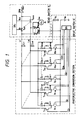
- Fig. 1 shows an equivalent circuit diagram of a conventional photoelectric converting device which has already been proposed by us.
- Light information which entered photoelectric conversion elements S1 ⁇ 1 to S36 ⁇ 48 are transmitted from the photoelectric conversion elements S1 ⁇ 1 to S36 ⁇ 48 through accumulation capacitors C s1-1 to C s36-48 , transfer TFTs T1 ⁇ 1 to T36 ⁇ 48, resetting TFTs R1 ⁇ 1 to R36 ⁇ 48, and matrix signal wirings L1 to L48 and become parallel voltage outputs. Further, the parallel voltage outputs are supplied to a read switch IC and become a serial signal. The serial signal is taken out to the outside.
- the photoelectric conversion elements of 1728 bits corresponding to the total number of pixels are divided into 36 blocks every 48 bits.
- the operations of the 36 blocks are sequentially executed on a block unit basis.
- Fig. 2 shows a timing chart when an original of a uniform image concentration is read by the conventional photoelectric converting device.
- the light information which entered the photoelectric conversion elements S1 ⁇ 1 to S1 ⁇ 48 of the first block are converted into photo currents and are accumulated as charges into the accumulation capacitors C s1-1 to C s1-48 .
- a first voltage pulse to transfer is applied to a gate drive line G1 for a time t1, thereby switching the transfer TFTs T1 ⁇ 1 to T1 ⁇ 48 to the on state.
- the charges in the accumulation capacitors C s1-1 to C s1-48 are transmitted through the matrix signal wirings L1 to L48 and are transferred to load capacitors C L1 to C L48 , so that potentials V L1 to V L48 of the load capacitors rise (transfer operation).
- a voltage pulse is sequentially supplied from a shift register SR2 to gate drive lines g1 to g48 and read switches T sw1 to T sw48 are sequentially switched to the on state, thereby converting the signals of the first block which were transferred to the load capacitors C L1 to C L48 into the serial signal.
- the serial signal is read out to the outside of the photoelectric converting apparatus.
- a voltage pulse C res to reset is supplied to reset switches R sw1 to R sw48 for a time t2, thereby resetting the load capacitors C L1 to C L48 .
- a voltage pulse is suppled to a gate drive line G2 and the transfer operation of the second block is started.
- the reset TFTs R1 ⁇ 1 to R1 ⁇ 48 are turned on, the charges in the accumulation capacitors C s1-1 to C s1-48 of the first block are reset, thereby preparing for the next read-out operation.
- the transfer operation, reading operation, and resetting operation are sequentially executed on a block unit basis as mentioned above. Therefore, the image signal from the photoelectric converting apparatus is intermittently generated as shown by V out in Fig. 2.
- the conventional photoelectric converting device As an image input section of a system such as a facsimile apparatus or the like, there is a case where a problem such that a processing circuit to convert the intermittent signals which are generated from the photoelectric converting apparatus into the continuous signal is needed and a correction circuit to execute a shading correction and the like becomes complicated occurs.
- Still another object of the invention is to provide a photoelectric converting device which can fully or substantially eliminate a period of time when a signal between blocks is not generated in a signal output of the photoelectric converting apparatus which is driven in a matrix manner and which can substantially raise a reading speed.
- Another object of the invention is to provide a photoelectric converting device having an advantage such that there is no need to perform processes for temporarily storing a signal output of the photoelectric converting apparatus into a line memory before it is image processed and for converting the intermittent signals into a continuous signal on the side of a system such as a facsimile apparatus or the like because a period of time when a signal between blocks is not generated in the signal output is eliminated or there is no need to non-continuously execute image processes, so that an increase in costs of the whole system and a deterioration in image quality are not caused.
- a photoelectric converting device comprising: a photoelectric converting section in which a plurality of photoelectric conversion elements, switching elements, matrix signal wirings, and gate drive wires are arranged on a same substrate and which generates parallel signals; a drive switching section for applying drive signals to the gate drive wirings; and a read switching section for converting the parallel signals which are transferred from the matrix signal wirings into a serial signal and reading out to an outside, wherein the read switching section is constructed by transfer switches connected to the matrix signal wirings, read capacitors, and read switches for reading out parallel signals as a serial signal from the read capacitors by being sequentially switched.
- the intermittent output which causes a problem in the conventional photoelectric converting apparatus which is matrix driven every block is solved and the period of time when the signal between blocks is not generated is eliminated, so that a reading speed of the photoelectric converting apparatus can be made substantially high.
- the photoelectric converting apparatus of the invention since image processes on the side of a system such as a facsimile apparatus or the like can be executed by simple means, there is an advantage such that an increase in costs of the whole system and a reduction in image quality are not caused.
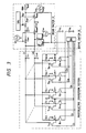
- Fig. 3 shows an equivalent circuit diagram of a photoelectric converting device as a preferred first embodiment according to the invention.
- a construction of a photoelectric conversion section comprising a photoelectric conversion element section, an accumulation capacitor section, a TFT section, a matrix signal wiring section, a gate drive wiring section, and the like which are formed on the same substrate is fundamentally similar to the equivalent circuit diagram of the conventional photoelectric converting apparatus shown in Fig. 1.
- the photoelectric converting device of the embodiment differs from the conventional photoelectric converting apparatus when it is seen as an equivalent circuit with respect to a read switch section in which transfer switches U sw1 to U sw48 and read capacitors C T1 to C T48 are provided between the load capacitors C L1 to C L48 and the read switches T sw1 to T sw48 in the matrix signal wiring section and a reset switch V sw to reset the read capacitors C T1 to C T48 is further provided.
- Transfer switches U sw1 to U sw48 are connected to the matrix signal wirings L1 to L48, respectively, and are used to transfer the charges accumulated in the load capacitors C L1 to C L48 formed on the matrix signal wirings L1 to L48 to the read capacitors C T1 to C T48 .
- the transfer switches U sw1 to U sw48 are simultaneously driven by a transfer pulse G t .
- the read switches T sw1 to T sw48 are connected to the read capacitors, respectively, and are used to sequentially read out potentials of the read capacitors C T1 to C T48 to the outside of the photoelectric converting apparatus through an amplifier Amp by sequentially switching the read switches.
- the read switches are sequentially driven by the shift register SR2.
- R sw1 to R sw48 denote the reset switches which are arranged between the load capacitors C L1 to C L48 and the transfer switches U sw1 to U sw48 which are formed in the matrix signal wiring section and are used to reset the potentials of the load capacitors C L1 to C L48 to a reset potential V R .
- the reset switches are driven by the reset pulse C res .
- V sw denotes the reset switch to reset the potentials of the read capacitors C T1 to C T48 to the reset potential V R .
- the reset switch V sw is driven by a reset pulse g res .
- Fig. 4 is a timing chart showing the reading operation of the photoelectric converting device of the first embodiment. It is now assumed that an original has a uniform image concentration.
- the light information which entered the photoelectric conversion elements S1 ⁇ 1 to S1 ⁇ 48 of the first block are accumulated as charges into the accumulation capacitors C s1-1 to C s1-48 .
- a voltage pulse is applied to the first gate drive line G1 from a shift register SR1, so that the transfer TFTs T1 ⁇ 1 to T1 ⁇ 48 are turned on.
- the charges of the accumulation capacitors C s1-1 to C s1-48 are transmitted through the matrix signal wirings L1 to L48 and are transferred to the load capacitors C L1 to C L48 .
- a gate pulse width t1 which is necessary for such a transfer of the charges depends on a time constant which is determined by smaller one of the capacitance values of the accumulation capacitor C s and the load capacitor C L and an ON resistance R t of the transfer TFT T.
- the accumulation capacitor C s is properly set to a value within a range from 10 to 20 pF.
- the load capacitor C L is properly set to a value within a range from 100 to 300 pF. Since the ON resistance R t of the TFT using a-Si:H is so large to be a few M ⁇ , the time constant is set to a value within a range from 10 to 40 ⁇ s.
- a length t3 of the gate pulse G t which is necessary for such a transfer of the charges depends on a time constant which is determined by an ON resistance R u of the transfer switch U sw and smaller one of the capacitance values of the load capacitor C L and the read capacitor C T .
- the load capacitor C L is properly set to a value within a range from 100 to 300 pF.
- the read capacitor C T is properly set to a value within a range from 10 to 20 pF. Since the ON resistance R u can be selected to a value within a range from 50 to 300 ⁇ if a general analog switch is used, the time constant can be set to a short value of 100 ns or less.
- the signal charges of the first block which were transferred to the read capacitors C T1 to C T48 are converted into the serial signal by the read switches T sw1 to T sw48 .
- the serial signal is amplified by the amplifier Amp and is taken out as an output voltage V out to the outside of the photoelectric converting apparatus.
- a period of time t4 when the signal output of one block is generated depends on the ON resistance R t of the read switch T sw , the input capacitance containing the wiring capacitance of the amplifier Amp, and the response speed of the amplifier. However, since the period t4 can be selected to a value within a range from 1 to 2 ⁇ s per bit, it is set to a value within a range from about 50 to 100 ⁇ s per 48 bits.
- the reset pulse g res is successively applied to the reset switch V sw for a latter half period of time t5 in the period of time when the voltage pulse which is applied to the gate drive lines g1 to g48 is set to the high voltage. Therefore, in the latter half period t5, both of the read switch T sw and the reset switch V sw are simultaneously turned on and the read capacitors C T1 to C T48 are sequentially reset to the reset potential V R .
- a length t5 of the gate pulse g res which is necessary to reset depends on a time constant which is determined by the ON resistance R v of the reset switch V sw , the ON resistance R t of the read switch T sw , and the capacitance value of the read capacitor C T .
- the value of the read capacitor C T is properly set to a value within a range from 10 to 20 pF. Since the ON resistances R V and R t can be selected to values within a range from 50 to 300 ⁇ if general analog switches are used, the time constant can be set to a short value of 100 ns or less.
- the load capacitors C L1 to C L48 are simultaneously reset by applying the reset pulse C res to the reset switches R sw1 to R sw48 in parallel with the above signal reading operation.
- a length t2 of the gate pulse C res which is needed to reset the load capacitors depends on a time constant which is determined by an ON resistance R r of the reset switch R sw , the resistance of the matrix signal wirings, and the capacitance values of the load capacitor C L .
- the length t2 is set to a value of about a few ⁇ s.
- a voltage pulse is applied to the gate drive wiring G2 from the shift register SR1 and the transfer operation of the second block is started. Simultaneously with the transfer operation, the reset TFTs R1 ⁇ 1 to R1 ⁇ 48 of the first block are turned on. The charges of the accumulation capacitors C s1-1 to C s1-48 of the first block are reset to the reset potential V R , thereby preparing for the next accumulating operation.
- a period of time when the signal between blocks is not generated in the signal output V out can be eliminated and the reading speed can be substantially made fast.
- the resetting operation of the load capacitors C L1 to C L48 and the transfer operation of the next block can be executed in parallel with the reading operation by the read switches T sw1 to T sw48 .
- a time which is required for the reading and resetting operations of one block is determined by either longer one of the sum (t1 + t2 + t3) of the period t1 when the transfer TFTs are in the ON state, the period t3 to transfer the charges to the read capacitors, and the period t2 to reset the load capacitors and the period t4 when the read switches T sw1 to T sw48 operate. Since the period t3 is substantially so short to be 100 ns or less as mentioned above, such a time is decided by either longer period of the period (t1 + t2) and the period t4.
- a time which is required to execute the reading and resetting operations of one block is determined by the sum (t1 + t2 + t4) of the period t1 when the transfer TFTs are in the ON state, the period t2 to reset the load capacitors, and the period t4 when the read switches T sw1 to T sw48 operate.
- the reading time per block is equal to 95 ⁇ s in the case of the conventional apparatus.
- the period t4 is determined by rate-determining step and is equal to 50 ⁇ s, so that the speed can be raised by about 50%.
- the reading time per block is set to a value which is equal to that in the conventional apparatus, that is, if it is set to 95 ⁇ s in the above example
- the period t4 when the read switches T sw1 to T sw48 operate can be changed from 50 ⁇ s to 95 ⁇ s and the sum (t1 + t2) of the period t1 when the transfer TFTs are in the ON state and the period t2 to reset the load capacitors can be set to a long time of 95 ⁇ s. Therefore, the ON resistances of the switches (TFTs and general analog switches) which restrict the respective periods can be set to large values, namely, the sizes of switches can be reduced. If there is no need to raise the read speed as mentioned above, there are advantages such that the chip size can be reduced and the switching noises can be reduced.
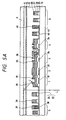
- Figs. 5A and 5B are a schematic cross sectional view and a schematic plan view of a photoelectric conversion section according to the photoelectric converting apparatus of the embodiment.
- a photoelectric conversion element section 1, an accumulation capacitor section 2, TFT sections 3 and 4, a matrix signal wiring section 5, a gate drive wiring section 6, and the like are integratedly formed on a translucent insulative substrate 10 by using a-Si:H by the same process.
- a first conductor layer 24 made of Al, Cr, or the like, a first insulative layer 25 made of SiN or the like, a photoconductive semiconductor layer 26 made of a-Si:H, an ohmic contact layer 27 made of n+ type a-Si:H, and a second conductor layer 28 made of Al, Cr, or the like are formed on the insulative substrate 10.
- reference numerals 30 and 31 denote upper layer electrode wirings.
- a signal light L' which was reflected by an original P changes a conductivity of the photoconductive semiconductor layer 26 made of a-Si:H and changes a current flowing between the upper layer electrode wirings 30 and 31 which face like a comb.
- Reference numeral 32 denotes a light shielding layer made of a metal.
- the light shielding layer 32 can be also constructed in a manner such that it is connected to a proper driving source and serves as a control electrode (gate electrode) which faces the main electrodes 30 (source electrode or drain electrode) and 31 (drain electrode or source electrode).
- the accumulation capacitor section 2 comprises: a lower layer electrode wiring 33; the first insulative layer 25 and the photoconductive semiconductor layer 26 which are formed on the lower layer electrode wiring 33; and a wiring which is formed on the photoconductive semiconductor layer 26 and is continuous with the upper layer electrode wiring 31 of the photoelectric conversion section 1.
- the accumulation capacitor section 2 has a structure of what is called an MIS capacitor. Any one of a positive bias and a negative bias can be used as a bias condition. However, by setting the bias condition so that the lower layer electrode wiring 33 is always set to a negative bias, a stable capacitance and stable frequency characteristics can be obtained.
- the TFT sections 3 and 4 comprise: a lower layer electrode wiring 34 serving as a gate electrode; the second insulative layer 25 serving as a gate insulative layer; the semiconductor layer 26; an upper layer electrode wiring 35 serving as a source electrode; an upper layer electrode wiring 36 serving as a drain electrode; and the like.
- an individual signal wiring 22 made of a first conductive layer, the insulative layer 25 which covers the individual signal wiring, the semiconductor layer 26, the ohmic contact layer 27, and a common signal wiring 37 which crosses the individual signal wiring and is made of a second conductor layer are sequentially laminated onto the substrate 10.
- Reference numeral 38 denotes a contact hole to obtain an ohmic contact between the individual signal wiring 22 and the common signal wiring 37.
- Reference numeral 39 denotes a line to line shield wiring provided between the common signal wirings.
- an individual gate wiring 40 made of the first conductor layer 24, the insulative layer 25 which covers the individual gate wiring, the semiconductor layer 26, the ohmic contact layer 27, and the common gate wiring 41 which crosses the individual gate wiring 40 and is made of the second conductor layer 28 are sequentially laminated onto the substrate 10.
- Reference numeral 42 denotes a contact hole to obtain an ohmic contact between the individual gate wiring 40 and the common gate wiring 41.
- the photoelectric conversion element section since all of the photoelectric conversion element section, accumulation capacitor section, TFT setion, matrix signal wiring section, and gate drive wiring section have the laminate structure of the photoconductive semiconductor layer, insulative layer, conductor layer, and the like, those sections are simultaneously formed by the same process.
- a passivation layer 11 made of SiN or the like to mainly protect and stabilize the semiconductor layer surfaces of the photoelectric conversion element section 1 and TFT sections 3 and 4 and a friction resistance layer 8 made of a microsheet glass or the like to protect the photoelectric conversion elements and the like from the friction with the original P are formed on the second conductor layer 28.
- a static electricity countermeasure layer 15 made of a translucent conductor layer is formed between the passivation layer 11 and the friction resistance layer 8.
- the static electricity countermeasure layer 15 is arranged to prevent that the static electricity which is generated by the friction between the original P and the friction resistance layer 8 exerts an adverse influence on the photoelectric conversion elements and the like.
- a transparent conductive film of an oxide semiconductor such as ITO or the like is used as a material of the static electricity countermeasure layer 15 because it is necessary to transmit an illumination light L and the signal light L'.
- the friction resistance layer formed with the static electricity countermeasure layer is adhered onto the passivation layer 11 by an adhesive layer.
- the embodiment uses a structure of the photoelectric converting apparatus of what is called a complete contact type in which the reflected light from an original is directly detected without using an equal magnification fiber lens array or the like.
- a system such as a facsimile apparatus or the like can be constructed as a fairly compact size and a degree of freedom in designing of the mechanism when a system is constructed increases.
- the invention can be also used in an image reading apparatus of the contact reading type using an equal magnification fiber lens and the like.
- Fig. 6 shows a preferred second embodiment according to the invention and shows an equivalent circuit diagram of only a parallel/serial converting section 12 because a photoelectric converting section is similar to that in the first embodiment shown in Fig. 1.
- a dummy load capacitor C L0 a transfer switch U sw0 to transfer charges of the dummy load capacitor C L0 , a read capacitor C T0 , a read switch T sw0 , a reset switch V sw0 to reset the read capacitor C T0 , and a reset switch R sw0 to reset the dummy load capacitor C L0 are added to the parallel/serial conversion section in the first embodiment.
- timing control circuit OR to drive the above additional circuits and buffer amplifiers Amp1 and Amp2 and a differential amplifier for obtaining a differential output between an output of the dummy load capacitor and an ordinary signal output are added.
- the reading operation of the second embodiment is executed as follows.
- the reset switch R sw0 By applying the reset pulse C res , the reset switch R sw0 operates simultaneously with the reset switches R sw1 to R sw48 and the dummy load capacitor C L0 is reset to the reset potential V R .
- the transfer pulse G t By applying the transfer pulse G t , the transfer switch U sw0 operates simultaneously with the transfer switches U sw1 t0 U sw48 .
- the charges in the dummy load capacitor C L0 are transferred to the read capacitor C T0 .
- the read switches T sw1 to T sw48 are sequentially turned on, thereby generating a signal output from the buffer amplifier Amp1.
- the read switch T sw0 is switched at timings when the OR of the gate pulses of the second gate drive lines g1 to g48 is calculated and a potential of the read capacitor C T0 is generated through the buffer amplifier Amp2.
- the read capacitor C T0 is reset to the reset potential V R by the reset switch V sw0 at the same timing as the timing when the read capacitor C T48 is reset.
- a dummy signal which is generated from the buffer amplifier Amp2 is ideally set to the reset potential V R .
- the switching noises of the switches are multiplexed.
- the switching noises of the switches are also multiplexed to the light information obtained by the photoelectric conversion section.
- the switching noises multiplexed to the dummy signal and the switching noises multiplexed to the light information can be substantially equalized by making the shapes and the like of the switches which are used coincident. Therefore, the switching noises can be cancelled by obtaining a difference between the dummy signal which is generated from the amplifier Amp2 and the signal which is generated from the amplifier Amp1.
- the photoelectric converting apparatus of the present invention can be also applied to a system such as facsimile apparatus, image reader, or the like to execute image processes of a high quality.
- Fig. 7 shows a preferred third embodiment according to the invention and shows another example of a construction of the parallel/serial conversion section in which a dummy signal is read out and a difference between the dummy signal and the inherent signal output is obtained, thereby cancelling the switching noises in a manner similar to the second embodiment.
- a power source for the reset potential V R is directly connected to the transfer switch U sw0 in place of the dummy load capacitor C L0 in the second embodiment. Since the transfer switch U sw0 is driven by the gate pulse G t , at the timing synchronized with the reading timing of each bit, the potential of the read capacitor C T0 is set to the reset potential V R . The read switch T sw0 is switched and the potential of the read capacitor C T0 is read out to the buffer amplifier Amp2 in a manner similar to the second embodiment. After that, the read capacitor C T0 is reset by the reset switch V sw0 at a timing of g res .
- Fig. 7 Since the construction shown in Fig. 7 doesn't need the dummy load capacitor C L0 of a large capacitance value within a range from 100 to 300 pF, the switching noises can be easily cancelled as compared with the method whereby the dummy load capacitor C L0 is used as shown in the second embodiment.
- the read capacitor C L0 is reset at a timing of each bit, there are advantages such that a fluctuation of the potential of the read capacitor C L0 due to a leakage current or the like can be reduced and an error in association with the noise cancel can be extremely reduced.
- Fig. 8 shows a preferred example of a facsimile apparatus which is constructed by using the photoelectric converting apparatus of the invention.
- Reference numeral 102 denotes a feed roller to feed the original P toward the reading position;
- 104 indicates a separating member to certainly separate and feed the originals P one by one;
- 106 a conveying roller which is arranged at the reading position for a photoelectric converting apparatus and restricts a surface of the original P to be read and conveys the original P.
- W denotes a recording medium having a form of a roll paper.
- Image information which was read by the photoelectric converting apparatus or image information which was transmitted from the outside is formed on the recording medium W.
- Reference numeral 110 denotes a recording head to form the image. Any one of various types of recording heads such as thermal head, ink jet recording head, and the like can be used as a recording head 110.
- an ink jet recording head for instance, there is preferably used a recording head of the type such that a film boiling phenomenon is caused in an ink by using a heat energy and a bubble is generated and the ink is emitted from an emission opening by the growth and contraction of the bubble.
- the recording head of either the serial type or the full-line type can be used.
- Reference numeral 112 denotes a platen roller for conveying the recording medium W toward the recording position by the recording head 110 and restricting the surface of the recording medium to be recorded.
- Reference numeral 120 denotes an operation panel in which switches to execute operation inputs, a display section to display messages and an operating state of the apparatus, and the like are arranged.
- Reference numeral 130 denotes a system control board. A control section to control each section, a processing circuit section of the image information, a transmitting and receiving section, and the like are provided on the board 130. Reference numeral 140 denotes a power source of the apparatus.
- the photoelectric converting apparatus of the invention as an image input section of the system such as a facsimile apparatus or the like, the image processes on the system side can be executed by simple means. Thus, the costs of the whole system can be remarkably reduced.
- the period of time when the signal between blocks is not generated in the signal output of the photoelectric converting apparatus which is matrix driven can be eliminated and the reading speed can be substantially made fast.
- the processes for temporarily storing the signal output of the photoelectric converting apparatus into the line memory before the signal output is image processed and for converting the intermittent signals into the continuous signal do not need to be executed on the side of the system such as a facsimile apparatus or the like or there is no need to non-continuously perform the image processes, so that there are advantages such that the costs of the whole system are not increased and the image quality is not deteriorated.
Landscapes
- Engineering & Computer Science (AREA)
- Multimedia (AREA)
- Signal Processing (AREA)
- Power Engineering (AREA)
- Physics & Mathematics (AREA)
- Computer Hardware Design (AREA)
- General Physics & Mathematics (AREA)
- Condensed Matter Physics & Semiconductors (AREA)
- Electromagnetism (AREA)
- Microelectronics & Electronic Packaging (AREA)
- Facsimile Heads (AREA)
- Transforming Light Signals Into Electric Signals (AREA)
- Light Receiving Elements (AREA)
- Measuring Pulse, Heart Rate, Blood Pressure Or Blood Flow (AREA)
- Indicating And Signalling Devices For Elevators (AREA)
- Drawing Aids And Blackboards (AREA)
Applications Claiming Priority (2)
| Application Number | Priority Date | Filing Date | Title |
|---|---|---|---|
| JP2028044A JP2911519B2 (ja) | 1990-02-06 | 1990-02-06 | 光電変換装置 |
| JP28044/90 | 1990-02-06 |
Publications (3)
| Publication Number | Publication Date |
|---|---|
| EP0441541A2 true EP0441541A2 (fr) | 1991-08-14 |
| EP0441541A3 EP0441541A3 (en) | 1992-02-26 |
| EP0441541B1 EP0441541B1 (fr) | 1996-09-25 |
Family
ID=12237747
Family Applications (1)
| Application Number | Title | Priority Date | Filing Date |
|---|---|---|---|
| EP91300806A Expired - Lifetime EP0441541B1 (fr) | 1990-02-06 | 1991-01-31 | Dispositif de conversion photoélectrique |
Country Status (8)
| Country | Link |
|---|---|
| US (1) | US5335094A (fr) |
| EP (1) | EP0441541B1 (fr) |
| JP (1) | JP2911519B2 (fr) |
| KR (1) | KR950009816B1 (fr) |
| AT (1) | ATE143554T1 (fr) |
| DE (1) | DE69122278T2 (fr) |
| MY (1) | MY107343A (fr) |
| TW (1) | TW223167B (fr) |
Families Citing this family (28)
| Publication number | Priority date | Publication date | Assignee | Title |
|---|---|---|---|---|
| JP3189990B2 (ja) * | 1991-09-27 | 2001-07-16 | キヤノン株式会社 | 電子回路装置 |
| JP3565453B2 (ja) | 1994-08-23 | 2004-09-15 | キヤノン株式会社 | 画像入出力装置 |
| US5812109A (en) * | 1994-08-23 | 1998-09-22 | Canon Kabushiki Kaisha | Image input/output apparatus |
| JPH0897965A (ja) * | 1994-09-29 | 1996-04-12 | Nec Corp | 密着型イメージセンサ |
| JP3183390B2 (ja) * | 1995-09-05 | 2001-07-09 | キヤノン株式会社 | 光電変換装置及びそれを用いた撮像装置 |
| JP3416351B2 (ja) | 1995-09-28 | 2003-06-16 | キヤノン株式会社 | 光電変換装置及びその駆動方法、それを用いたx線撮像装置及びその駆動方法 |
| US6127684A (en) * | 1996-02-26 | 2000-10-03 | Canon Kabushiki Kaisha | Photoelectric conversion apparatus and driving method of the apparatus |
| US6448561B1 (en) | 1996-02-26 | 2002-09-10 | Canon Kabushiki Kaisha | Photoelectric conversion apparatus and driving method of the apparatus |
| JP4654321B2 (ja) * | 1996-03-13 | 2011-03-16 | キヤノン株式会社 | 光電変換装置、x線撮像装置、及び該装置を有するシステム |
| JP4597171B2 (ja) * | 1996-03-13 | 2010-12-15 | キヤノン株式会社 | 光電変換装置、x線撮像装置、及び該装置を有するシステム |
| JP4035194B2 (ja) | 1996-03-13 | 2008-01-16 | キヤノン株式会社 | X線検出装置及びx線検出システム |
| US5841180A (en) * | 1996-03-27 | 1998-11-24 | Canon Kabushiki Kaisha | Photoelectric conversion device, method of driving photoelectric conversion device, and system having the device |
| JP4100739B2 (ja) * | 1996-10-24 | 2008-06-11 | キヤノン株式会社 | 光電変換装置 |
| JP3847889B2 (ja) | 1997-04-08 | 2006-11-22 | キヤノン株式会社 | 光電変換装置 |
| JP3805100B2 (ja) * | 1997-04-10 | 2006-08-02 | キヤノン株式会社 | 光電変換装置 |
| JP3636579B2 (ja) | 1997-11-04 | 2005-04-06 | キヤノン株式会社 | 光電変換装置、光電変換装置の駆動方法及びその光電変換装置を有するシステム |
| US7129985B1 (en) | 1998-11-24 | 2006-10-31 | Canon Kabushiki Kaisha | Image sensing apparatus arranged on a single substrate |
| JP4181703B2 (ja) * | 1999-09-02 | 2008-11-19 | キヤノン株式会社 | 光電変換装置 |
| JP3984808B2 (ja) | 2000-09-07 | 2007-10-03 | キヤノン株式会社 | 信号処理装置及びそれを用いた撮像装置並びに放射線撮像システム |
| JP4208491B2 (ja) * | 2002-06-11 | 2009-01-14 | キヤノン株式会社 | 撮像装置及び指紋認識装置 |
| US8005918B2 (en) | 2002-11-12 | 2011-08-23 | Rateze Remote Mgmt. L.L.C. | Data storage devices having IP capable partitions |
| US7620981B2 (en) | 2005-05-26 | 2009-11-17 | Charles William Frank | Virtual devices and virtual bus tunnels, modules and methods |
| US8819092B2 (en) | 2005-08-16 | 2014-08-26 | Rateze Remote Mgmt. L.L.C. | Disaggregated resources and access methods |
| US20080308585A1 (en) * | 2006-09-27 | 2008-12-18 | John Foley | Nozzle |
| GB2446199A (en) | 2006-12-01 | 2008-08-06 | David Irvine | Secure, decentralised and anonymous peer-to-peer network |
| JP5017025B2 (ja) * | 2007-08-31 | 2012-09-05 | キヤノン株式会社 | 光電変換装置の駆動方法 |
| JP5606182B2 (ja) * | 2010-06-30 | 2014-10-15 | キヤノン株式会社 | 固体撮像装置 |
| JP5763373B2 (ja) * | 2011-03-09 | 2015-08-12 | 理想科学工業株式会社 | 画像形成装置 |
Citations (6)
| Publication number | Priority date | Publication date | Assignee | Title |
|---|---|---|---|---|
| JPS55132254A (en) * | 1979-04-02 | 1980-10-14 | Canon Inc | Recorder |
| JPS57207487A (en) * | 1981-06-16 | 1982-12-20 | Matsushita Electric Ind Co Ltd | Solid-state image pickup device |
| JPS5912666A (ja) * | 1982-07-12 | 1984-01-23 | Sanyo Electric Co Ltd | インクジエツトフアクシミリ |
| JPS62155666A (ja) * | 1985-12-27 | 1987-07-10 | Mitsubishi Metal Corp | 電子黒板 |
| EP0233020A2 (fr) * | 1986-02-04 | 1987-08-19 | Canon Kabushiki Kaisha | Appareil à matrice à interrupteurs utilisé dans un dispositif de conversion photoélectrique |
| JPS63214084A (ja) * | 1987-03-02 | 1988-09-06 | Semiconductor Res Found | 固体撮像装置の信号読み出し方法 |
Family Cites Families (8)
| Publication number | Priority date | Publication date | Assignee | Title |
|---|---|---|---|---|
| JPS61120570A (ja) * | 1984-11-16 | 1986-06-07 | Ricoh Co Ltd | 画像読取装置 |
| KR900003772B1 (ko) * | 1984-11-28 | 1990-05-31 | 가부시끼가이샤 도시바 | 이미지 센서(image sensor) |
| US4788445A (en) * | 1986-01-24 | 1988-11-29 | Canon Kabushiki Kaisha | Long array photoelectric converting apparatus with insulated matrix wiring |
| JPS639358A (ja) * | 1986-06-30 | 1988-01-16 | Fuji Xerox Co Ltd | 原稿読取装置 |
| JPH0748785B2 (ja) * | 1986-07-04 | 1995-05-24 | キヤノン株式会社 | 信号読み出し方法 |
| JPS6457659A (en) * | 1987-05-18 | 1989-03-03 | Fuji Electric Co Ltd | Linear image sensor |
| JPH0693749B2 (ja) * | 1989-02-14 | 1994-11-16 | 富士ゼロックス株式会社 | イメージセンサのクロストーク補正方法 |
| JPH0491556A (ja) * | 1990-08-06 | 1992-03-25 | Fuji Xerox Co Ltd | 読み取り装置 |
-
1990
- 1990-02-06 JP JP2028044A patent/JP2911519B2/ja not_active Expired - Fee Related
-
1991
- 1991-01-31 AT AT91300806T patent/ATE143554T1/de not_active IP Right Cessation
- 1991-01-31 DE DE69122278T patent/DE69122278T2/de not_active Expired - Fee Related
- 1991-01-31 EP EP91300806A patent/EP0441541B1/fr not_active Expired - Lifetime
- 1991-02-02 TW TW080100848A patent/TW223167B/zh active
- 1991-02-05 MY MYPI91000169A patent/MY107343A/en unknown
- 1991-02-06 KR KR1019910002004A patent/KR950009816B1/ko not_active IP Right Cessation
-
1993
- 1993-03-01 US US08/026,107 patent/US5335094A/en not_active Expired - Fee Related
Patent Citations (6)
| Publication number | Priority date | Publication date | Assignee | Title |
|---|---|---|---|---|
| JPS55132254A (en) * | 1979-04-02 | 1980-10-14 | Canon Inc | Recorder |
| JPS57207487A (en) * | 1981-06-16 | 1982-12-20 | Matsushita Electric Ind Co Ltd | Solid-state image pickup device |
| JPS5912666A (ja) * | 1982-07-12 | 1984-01-23 | Sanyo Electric Co Ltd | インクジエツトフアクシミリ |
| JPS62155666A (ja) * | 1985-12-27 | 1987-07-10 | Mitsubishi Metal Corp | 電子黒板 |
| EP0233020A2 (fr) * | 1986-02-04 | 1987-08-19 | Canon Kabushiki Kaisha | Appareil à matrice à interrupteurs utilisé dans un dispositif de conversion photoélectrique |
| JPS63214084A (ja) * | 1987-03-02 | 1988-09-06 | Semiconductor Res Found | 固体撮像装置の信号読み出し方法 |
Non-Patent Citations (5)
| Title |
|---|
| PATENT ABSTRACTS OF JAPAN vol. 11, no. 390 (E-567)(2837) 19 December 1987, & JP-A-62 155666 (MITSUBISHI METAL CORP) 10 July 1987, * |
| PATENT ABSTRACTS OF JAPAN vol. 13, no. 2 (E-700)(3350) 06 January 1989, & JP-A-63 214084 (SEMICONDUCTOR RES FOUND) 06 September 1988, * |
| PATENT ABSTRACTS OF JAPAN vol. 4, no. 187 (M-048) 23 December 1980, & JP-A-55 132254 (CANON INC) 14 October 1980, * |
| PATENT ABSTRACTS OF JAPAN vol. 7, no. 62 (E-164) 15 March 1983, & JP-A-57 207487 (MATSUSHITA DENKI SANGYO KK) 20 December 1982, * |
| PATENT ABSTRACTS OF JAPAN vol. 8, no. 95 (E-242)(1532) 02 May 1984, & JP-A-59 012666 (SANYO DENKI K.K.) 23 January 1984, * |
Also Published As
| Publication number | Publication date |
|---|---|
| EP0441541A3 (en) | 1992-02-26 |
| MY107343A (en) | 1995-11-30 |
| DE69122278D1 (de) | 1996-10-31 |
| TW223167B (fr) | 1994-05-01 |
| JPH03231560A (ja) | 1991-10-15 |
| ATE143554T1 (de) | 1996-10-15 |
| KR910016087A (ko) | 1991-09-30 |
| KR950009816B1 (ko) | 1995-08-28 |
| US5335094A (en) | 1994-08-02 |
| DE69122278T2 (de) | 1997-02-13 |
| JP2911519B2 (ja) | 1999-06-23 |
| EP0441541B1 (fr) | 1996-09-25 |
Similar Documents
| Publication | Publication Date | Title |
|---|---|---|
| US5335094A (en) | Photoelectric converting device having matrix wiring and read-out of parallel signals as a serial signal | |
| EP0484926B1 (fr) | Dispositif de lecture d'images transférant la charge de remise à zéro d'un élement accumulatif de charges à travers l'élément photosensible associé | |
| US4967067A (en) | Signal read-out circuit which lowers diffusion capacitance by limiting emitting current with resistive elements | |
| EP0977268A2 (fr) | Appareil de conversion photo-électrique, sa méthode de commande, et appareil de traitment de l'information utilisant celui-ci | |
| JPH11150255A (ja) | 光電変換装置 | |
| US5162644A (en) | Contact type image sensor having photoelectric conversion elements to reduce signal variation caused by luminous intensity variation of light source | |
| EP0233489B1 (fr) | Méthode pour adresser au moins un pixel photosensible ou un pixel de cristal liquide dans un réseau matriciel | |
| EP0576040B1 (fr) | Convertisseur photoélectrique | |
| US4788445A (en) | Long array photoelectric converting apparatus with insulated matrix wiring | |
| US5856666A (en) | Multiplexer circuit | |
| JPH077608A (ja) | 情報通信端末器の一体型入出力装置 | |
| JPH06245031A (ja) | 画像読取装置及び画像読取方法 | |
| KR940006933B1 (ko) | 콘택 영상 센서 | |
| JP4181703B2 (ja) | 光電変換装置 | |
| EP0449588A1 (fr) | Méthode de commande d'un senseur optique du type transistor à couche mince et son circuit de commande | |
| JPH0537714A (ja) | 光電変換装置 | |
| US5264938A (en) | Image sensor | |
| KR100316071B1 (ko) | X선 촬영장치 | |
| US5138467A (en) | Photoelectric conversion device | |
| JPH0584971B2 (fr) | ||
| JP4646997B2 (ja) | 光電変換装置の駆動方法 | |
| JPH05167775A (ja) | 2次元密着型イメージセンサ及びその駆動方法 | |
| JPH0328870B2 (fr) | ||
| JPH022303B2 (fr) | ||
| JPH08139852A (ja) | イメージセンサの駆動方法 |
Legal Events
| Date | Code | Title | Description |
|---|---|---|---|
| PUAI | Public reference made under article 153(3) epc to a published international application that has entered the european phase |
Free format text: ORIGINAL CODE: 0009012 |
|
| AK | Designated contracting states |
Kind code of ref document: A2 Designated state(s): AT BE CH DE DK ES FR GB GR IT LI LU NL SE |
|
| PUAL | Search report despatched |
Free format text: ORIGINAL CODE: 0009013 |
|
| AK | Designated contracting states |
Kind code of ref document: A3 Designated state(s): AT BE CH DE DK ES FR GB GR IT LI LU NL SE |
|
| 17P | Request for examination filed |
Effective date: 19920716 |
|
| 17Q | First examination report despatched |
Effective date: 19940526 |
|
| GRAH | Despatch of communication of intention to grant a patent |
Free format text: ORIGINAL CODE: EPIDOS IGRA |
|
| GRAA | (expected) grant |
Free format text: ORIGINAL CODE: 0009210 |
|
| GRAH | Despatch of communication of intention to grant a patent |
Free format text: ORIGINAL CODE: EPIDOS IGRA |
|
| AK | Designated contracting states |
Kind code of ref document: B1 Designated state(s): AT BE CH DE DK ES FR GB GR IT LI LU NL SE |
|
| PG25 | Lapsed in a contracting state [announced via postgrant information from national office to epo] |
Ref country code: NL Free format text: LAPSE BECAUSE OF FAILURE TO SUBMIT A TRANSLATION OF THE DESCRIPTION OR TO PAY THE FEE WITHIN THE PRESCRIBED TIME-LIMIT Effective date: 19960925 Ref country code: LI Effective date: 19960925 Ref country code: GR Free format text: LAPSE BECAUSE OF FAILURE TO SUBMIT A TRANSLATION OF THE DESCRIPTION OR TO PAY THE FEE WITHIN THE PRESCRIBED TIME-LIMIT Effective date: 19960925 Ref country code: ES Free format text: THE PATENT HAS BEEN ANNULLED BY A DECISION OF A NATIONAL AUTHORITY Effective date: 19960925 Ref country code: DK Effective date: 19960925 Ref country code: CH Effective date: 19960925 Ref country code: BE Effective date: 19960925 Ref country code: AT Effective date: 19960925 |
|
| REF | Corresponds to: |
Ref document number: 143554 Country of ref document: AT Date of ref document: 19961015 Kind code of ref document: T |
|
| REF | Corresponds to: |
Ref document number: 69122278 Country of ref document: DE Date of ref document: 19961031 |
|
| ITF | It: translation for a ep patent filed |
Owner name: SOCIETA' ITALIANA BREVETTI S.P.A. |
|
| PG25 | Lapsed in a contracting state [announced via postgrant information from national office to epo] |
Ref country code: SE Effective date: 19961225 |
|
| ET | Fr: translation filed | ||
| PG25 | Lapsed in a contracting state [announced via postgrant information from national office to epo] |
Ref country code: LU Free format text: LAPSE BECAUSE OF NON-PAYMENT OF DUE FEES Effective date: 19970131 |
|
| NLV1 | Nl: lapsed or annulled due to failure to fulfill the requirements of art. 29p and 29m of the patents act | ||
| REG | Reference to a national code |
Ref country code: CH Ref legal event code: PL |
|
| PLBE | No opposition filed within time limit |
Free format text: ORIGINAL CODE: 0009261 |
|
| STAA | Information on the status of an ep patent application or granted ep patent |
Free format text: STATUS: NO OPPOSITION FILED WITHIN TIME LIMIT |
|
| 26N | No opposition filed | ||
| REG | Reference to a national code |
Ref country code: GB Ref legal event code: IF02 |
|
| PGFP | Annual fee paid to national office [announced via postgrant information from national office to epo] |
Ref country code: GB Payment date: 20040119 Year of fee payment: 14 |
|
| PGFP | Annual fee paid to national office [announced via postgrant information from national office to epo] |
Ref country code: DE Payment date: 20040123 Year of fee payment: 14 |
|
| PGFP | Annual fee paid to national office [announced via postgrant information from national office to epo] |
Ref country code: FR Payment date: 20040126 Year of fee payment: 14 |
|
| PG25 | Lapsed in a contracting state [announced via postgrant information from national office to epo] |
Ref country code: IT Free format text: LAPSE BECAUSE OF NON-PAYMENT OF DUE FEES;WARNING: LAPSES OF ITALIAN PATENTS WITH EFFECTIVE DATE BEFORE 2007 MAY HAVE OCCURRED AT ANY TIME BEFORE 2007. THE CORRECT EFFECTIVE DATE MAY BE DIFFERENT FROM THE ONE RECORDED. Effective date: 20050131 Ref country code: GB Free format text: LAPSE BECAUSE OF NON-PAYMENT OF DUE FEES Effective date: 20050131 |
|
| PG25 | Lapsed in a contracting state [announced via postgrant information from national office to epo] |
Ref country code: DE Free format text: LAPSE BECAUSE OF NON-PAYMENT OF DUE FEES Effective date: 20050802 |
|
| GBPC | Gb: european patent ceased through non-payment of renewal fee |
Effective date: 20050131 |
|
| PG25 | Lapsed in a contracting state [announced via postgrant information from national office to epo] |
Ref country code: FR Free format text: LAPSE BECAUSE OF NON-PAYMENT OF DUE FEES Effective date: 20050930 |
|
| REG | Reference to a national code |
Ref country code: FR Ref legal event code: ST |