EP0435331B1 - Halbleitervorrichtung mit einem lateralen Bipolartransistor und entsprechende Herstellungsverfahren - Google Patents
Halbleitervorrichtung mit einem lateralen Bipolartransistor und entsprechende Herstellungsverfahren Download PDFInfo
- Publication number
- EP0435331B1 EP0435331B1 EP90125702A EP90125702A EP0435331B1 EP 0435331 B1 EP0435331 B1 EP 0435331B1 EP 90125702 A EP90125702 A EP 90125702A EP 90125702 A EP90125702 A EP 90125702A EP 0435331 B1 EP0435331 B1 EP 0435331B1
- Authority
- EP
- European Patent Office
- Prior art keywords
- region
- emitter
- collector
- bipolar transistor
- transistor
- Prior art date
- Legal status (The legal status is an assumption and is not a legal conclusion. Google has not performed a legal analysis and makes no representation as to the accuracy of the status listed.)
- Expired - Lifetime
Links
Images


Classifications
-
- H—ELECTRICITY
- H10—SEMICONDUCTOR DEVICES; ELECTRIC SOLID-STATE DEVICES NOT OTHERWISE PROVIDED FOR
- H10D—INORGANIC ELECTRIC SEMICONDUCTOR DEVICES
- H10D48/00—Individual devices not covered by groups H10D1/00 - H10D44/00
- H10D48/30—Devices controlled by electric currents or voltages
- H10D48/32—Devices controlled by only the electric current supplied, or only the electric potential applied, to an electrode which does not carry the current to be rectified, amplified or switched
- H10D48/34—Bipolar devices
-
- H—ELECTRICITY
- H10—SEMICONDUCTOR DEVICES; ELECTRIC SOLID-STATE DEVICES NOT OTHERWISE PROVIDED FOR
- H10D—INORGANIC ELECTRIC SEMICONDUCTOR DEVICES
- H10D10/00—Bipolar junction transistors [BJT]
- H10D10/01—Manufacture or treatment
- H10D10/061—Manufacture or treatment of lateral BJTs
-
- H—ELECTRICITY
- H10—SEMICONDUCTOR DEVICES; ELECTRIC SOLID-STATE DEVICES NOT OTHERWISE PROVIDED FOR
- H10D—INORGANIC ELECTRIC SEMICONDUCTOR DEVICES
- H10D10/00—Bipolar junction transistors [BJT]
- H10D10/60—Lateral BJTs
-
- H—ELECTRICITY
- H10—SEMICONDUCTOR DEVICES; ELECTRIC SOLID-STATE DEVICES NOT OTHERWISE PROVIDED FOR
- H10D—INORGANIC ELECTRIC SEMICONDUCTOR DEVICES
- H10D84/00—Integrated devices formed in or on semiconductor substrates that comprise only semiconducting layers, e.g. on Si wafers or on GaAs-on-Si wafers
- H10D84/01—Manufacture or treatment
- H10D84/0112—Integrating together multiple components covered by H10D8/00, H10D10/00 or H10D18/00, e.g. integrating multiple BJTs
- H10D84/0114—Integrating together multiple components covered by H10D8/00, H10D10/00 or H10D18/00, e.g. integrating multiple BJTs the components including vertical BJTs and lateral BJTs
-
- H—ELECTRICITY
- H10—SEMICONDUCTOR DEVICES; ELECTRIC SOLID-STATE DEVICES NOT OTHERWISE PROVIDED FOR
- H10D—INORGANIC ELECTRIC SEMICONDUCTOR DEVICES
- H10D84/00—Integrated devices formed in or on semiconductor substrates that comprise only semiconducting layers, e.g. on Si wafers or on GaAs-on-Si wafers
- H10D84/01—Manufacture or treatment
- H10D84/02—Manufacture or treatment characterised by using material-based technologies
- H10D84/03—Manufacture or treatment characterised by using material-based technologies using Group IV technology, e.g. silicon technology or silicon-carbide [SiC] technology
- H10D84/038—Manufacture or treatment characterised by using material-based technologies using Group IV technology, e.g. silicon technology or silicon-carbide [SiC] technology using silicon technology, e.g. SiGe
Definitions
- the present invention relates to a semiconductor device including a lateral bipolar junction transistor and a method of fabricating the same.
- a known very-high-speed bipolar junction transistor has a base contact electrode and an emitter contact electrode formed of a polycrystalline silicon film, and a base region and an emitter region formed by the diffusion of the impurity from the polycrystalline silicon film forming the emitter contact electrode in a self-alignment mode.
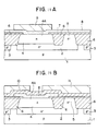
- Figs. 14A, 14B, 14C and 14D show the very-high-speed bipolar junction transistor in different steps of the fabricating process. As shown in Fig.
- an n-type epitaxial layer 4 is formed after forming an embedded collector region 2 of a second conductivity type, for example, n-type, and a p-type channel stop region 3 in one of the major surfaces of a silicon substrate 1 of a first conductivity type, for example, p-type, a heavily doped n-type collector contact region 5 is formed so as to reach the embedded collector region 2, and then a field insulating film 6 is formed by local oxidation over the entire surface excluding the collector electrode region, and a region 4A in which a base region and an emitter region are to be formed afterward.
- a second conductivity type for example, n-type
- a p-type channel stop region 3 in one of the major surfaces of a silicon substrate 1 of a first conductivity type, for example, p-type
- a heavily doped n-type collector contact region 5 is formed so as to reach the embedded collector region 2
- a field insulating film 6 is formed by local oxidation over the entire surface excluding
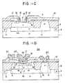
- a SiO 2 film 10 is formed over the entire surface including the patterned p + -type polycrystalline silicon film 8 by a CVD process, and then a second resist mask 11 is formed. Portions of the SiO 2 film 10 and the p + -type polycrystalline silicon film 8 corresponding to an active region, in which an intrinsic base region and an emitter region are to be formed, are removed by selective etching using the resist mask 11 to form a window 13 and a base contact electrode 12 formed of the p + -type polycrystalline silicon film 8.
- the region 4A is doped through the window 13 with a p-type impurity, i.e., boron, by ion implantation to form a link base region 14 for connecting an external base region and an intrinsic base region to be formed on the region 4A afterward.
- a SiO 2 film is formed by a CVD process, and then the SiO 2 film formed by the CVD process is densified through a heat treatment in which the SiO 2 film is heated at a temperature on the order of 900°C.
- boron contained in the base contact electrode 12 formed of the p + -type polycrystalline silicon film is caused to diffuse into the region 4A to form part of an external base region 16. Then, a SiO 2 side wall 15 is formed over the inner surface of the base electrode 12 facing the window 13.
- a second polycrystalline silicon film 18 for an emitter contact electrode is deposited by a CVD process in a window 17 defined by the side wall 15.
- the polycrystalline silicon film 18 is doped by ion implantation with a p-type impurity, such as B or BF 2 , and annealed to form a p-type intrinsic base region 19 in the active region, and then, the p-type base region 19 is doped by ion implantation with an n-type impurity, such as As, and annealed to form an n-type emitter region 20.
- a p-type impurity such as B or BF 2
- the polycrystalline silicon film 18 is doped by ion implantation with p-type and n-type impurities and annealed to form the p-type intrinsic base region 19 and the n-type emitter region 20.
- boron contained in the base contact electrode 12 formed of p + -type polycrystalline silicon is caused to diffuse to complete the external base region 16.
- the impurity concentration of the intrinsic base region 19 is higher than that of the link base region 14.
- contact holes are formed, and then a base electrode 21, a collector electrode 22 and an emitter electrode 23 of a metal, such as aluminum, are formed to complete a very-high-speed bipolar transistor 24.
- Fig. 10 shows the structure of a lateral pnp bipolar junction transistor 40.
- the lateral pnp bipolar junction transistor 40 is constructed by forming an n-type epitaxial layer 4 over an n-type embedded base region 26 formed on a p-type silicon substrate 1, forming a field insulating film 6 by selective oxidation, forming an n-type plug-in region 27 reaching the n-type embedded base region 26, and an n-type contact base region 28, forming a p-type collector region 32 and a p-type emitter region 33 respectively having heavily doped p-type regions 30 and 21, and forming an aluminum collector electrode 34, an aluminum base-electrode 35 and an aluminum emitter electrode 36.
- Fig. 10 shows the structure of a lateral pnp bipolar junction transistor 40.
- the lateral pnp bipolar junction transistor 40 is constructed by forming an n-type epitaxial layer 4 over an n-type embedded base region 26 formed on a p-type silicon substrate
- a p-type isolating region indicated at 37 is a p-type isolating region, at 38 is a layer insulating film and at 39 is a thin SiO 2 film.
- the p-type collector region 32 and the p-type emitter region are formed at the same time with the p-type intrinsic base region 19 of the npn bipolar junction transistor 24 shown in Fig. 14D, and the heavily doped p-type regions 30 and 31 are formed at the same time with the external base region 16 of the npn bipolar junction transistor 24.
- the base width W B is determined by the p-type collector region 32 and the p-type emitter region 33.
- Fig. 11 shows the impurity concentration profile of a section along an alternate long and short dash line 41.
- the impurity concentration profile has a peak at a position corresponding to a portion near the surface of the substrate as shown in Fig. 11, because the surface is doped by ion implantation with boron and boron is caused to diffuse in forming the p-type collector region 32 and the p-type emitter region 33. Accordingly, the collector region 32 and the emitter region are nearest in the vicinity of the surface.
- Fig. 12 shows the structure of another lateral pnp bipolar junction transistor 42, in which portions corresponding to those of the lateral pnp bipolar junction transistor shown in Fig. 10 are denoted by the same reference characters and the description thereof will be omitted to avoid duplication.
- a contact base region 28 is formed simultaneously with the contact collector region 5 of the npn bipolar junction transistor 24 shown in Fig. 14D, and a p-type emitter region 33 and a p-type collector region 32 are formed simultaneously with the external base region 16 of the npn bipolar junction transistor 24 through the diffusion of boron from a contact electrodes 44 and 43 formed of p + -type polycrystalline silicon.
- Indicated at 3 is a p-type channel stop region.
- the current amplification factor h FE of the lateral pnp trans istor 40 shown in Fig. 10 is reduced due to surface recombination because the current flows mainly along the surface, i.e., the vicinity of the interface of the SiO 2 film 39, and the current amplification factor h FE is liable to be unstable due to the variation of the surface recombination electrode depending on the condition of the interface of the SiO 2 film 39.
- Patent Abstracts of Japan, vol.5, no.125 (E-69)(797), August 12, 1981 & JP-A-56-62361 discloses a lateral pnp transistor in which the current flows mainly along the surface of the device.
- the present invention is intended to prevent surface recombination in a semiconductor device including a lateral bipolar junction transistor having a collector region, a base region and an emitter region formed in a lateral arrangement on a semiconductor substrate and to improve and stabilize the current amplification factor of the lateral bipolar junction transistor by forming the respective portions having peak impurity concentrations of the collector region and the emitter region within the base region.
- a semiconductor device in accordance with the present invention is set out in claim 1.
- a method of fabricating a semiconductor device in accordance with the present invention is furthermore set out in any one of claims 3 and 4.
- the present invention reduces the base width W B to provide a high f T and a high h FE .
- a semiconductor device in accordance with the present invention comprises a semiconductor substrate 1 provided with a collector region 62, a base region 60 and an emitter region 61 in a lateral arrangement, wherein respective portions having peak impurity concentrations of the collector region and the emitter region are formed within the base region 60 and not near the surface.
- a method of fabricating a semiconductor device in accordance with the present invention comprises a step of forming a collector region 132 of a second conductivity type and an emitter region 133 of the second conductivity type in a lateral arrangement in a semiconductor substrate 1 of a first conductivity type by using a first mask 123 provided with a pair of openings 121 and 122; and a step of forming heavily doped regions 130 and 131 of the second conductivity type so as to be connected respectively to the collector region 132 and the emitter region 133 by using a second mask 127 provided with a pair of openings separated from each other by a distance d 2 greater than the distance d 1 between the openings of the first mask 123.
- the collector region 62 and emitter region 61 of the lateral transistor are formed so that portions thereof having the maximum impurity concentration are formed within the base region 60 to form a main current path within the base region 60 instead of near the surface of the same, which prevents the reduction of h FE due to surface recombination.
- the small variation of the surface recombination current due to the condition of the surface of the oxide film stabilizes the h FE .
- the lateral transistor has a stable, high h FE .
- the collector region 132 and the emitter region 133 are formed by using the first mask 123, and the heavily doped regions 130 and 131 of the collector region and the emitter region are formed by using a second mask 127. Accordingly, the pair of openings 121 and 122 of the first mask 123 can be separated from each other by the distance d 1 corresponding to the minimum line width which can be achieved by lithography. Accordingly, the collector region 132 and the emitter region 133 can be formed so that the base width W E corresponds to the minimum line width to achieve a high f T . Since the collector electrodes 43 and 134 and the emitter electrodes 44 and 136 are formed by using the second mask provided with the openings 125 and 126, the collector electrodes 43 and 134 and the emitter electrodes 44 and 136 can easily be isolated from each other.
- the emitter region 133 has a heavily doped region 131, the emitter injection efficiency is high and the h FE is improved.
- a lateral transistor having a high f T and a high h FE can be fabricated.
- Fig. 1 shows a lateral pnp transistor in a first embodiment according to the present invention.
- an embedded n-type base region 26 and an n-type epitaxial layer 4 are formed on a p-type silicon substrate 1, a p-type isolation region 37, and a selectively oxidized (LOCOS) field insulating layer 6 are formed and n-type plug-in region 27 reaching the embedded n-type base region 26, and an n-type base contact region 28 are formed.
- LOC selectively oxidized
- a p-type emitter region 61 and a p-type collector region 62 are formed in a lateral arrangement so that portions thereof respectively having maximum impurity concentrations are within the n-type epitaxial layer 4, which serves as a base region 60, with a distance corresponding to a base width W B therebetween, and then heavily doped p-type regions 63 and 64 are formed so as to be joined respectively to the emitter region 61 and the collector region 62. Subsequently, a layer insulating film 38 is formed, and then a collector electrode 34, a base electrode 35 and an emitter electrode 36, such as aluminum electrodes, are formed in contact holes to complete a lateral pnp bipolar transistor 65.
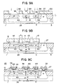
- Fig. 2 shows the variation of impurity concentration with depth along the line A 1 -A 1 in Fig. 1
- Fig. 3 shows the variation of impurity concentration with depth along the line B 1 -B 1 in Fig. 1.
- Figs. 4A, 4B, 4C and 4D are sectional views showing the lateral pnp bipolar transistor 65 in different steps of a fabricating process.
- the lateral pnp bipolar transistor 65 is fabricated together with a low emitter concentration transistor (LEC) featured by its high V EBO , low C BE and low noise.
- LEC low emitter concentration transistor
- an embedded n-type base region 26 and an embedded n-type collector region 68 are formed respectively in a lateral pnp transistor forming section 66 and a LEC transistor forming section 67 of a p-type silicon substrate 1, an n-type epitaxial layer 4 is formed, and then p-type isolation regions 37 and a field insulating layer 6 are formed.
- an n-type plug-in region 27 reaching the embedded n-type base region 26, and an n-type plug-in region 69 reaching the embedded n-type collector region 68 are formed respectively in the sections 66 and 67.
- Indicated at 80 is a thin SiO 2 film.
- a p-type emitter region 61 and a p-type collector regions 62 are formed in the section 66 so that portions thereof having maximum impurity concentrations are formed within the epitaxial layer 4, which serves as a base region, and, simultaneously, a p-type base region 83 for the LEC transistor is formed in the section 67 by ion implantation using a p-type impurity 82, such as boron, a resist mask 81 and energy of 180 keV or higher.
- a p-type impurity 82 such as boron
- a resist mask 81 such as boron
- heavily doped p-type regions 64 and 63 i.e., a p-type collector contact region and a p-type emitter contact region, are formed in the section 66 and, at the same time, a p-type base contact region 84 for the LEC transistor is formed in the section 67.
- An n-type emitter region 85 for the LEC transistor is formed in the section 67.
- An n-type collector contact region 86 for the LEC transistor is formed and an n-type base contact region 28 for the lateral pnp transistor is formed in the section 66 simultaneously with the formation of the n-type emitter region.
- contact holes are formed after forming a layer insulating film 38, and then collector electrode 34 and a base electrode 35 and an emitter electrode 36, such as aluminum electrodes, are formed in the section 66 to complete the lateral pnp bipolar transistor 65 and a collector electrode 87, a base electrode 88 and an emitter electrode 89, such as aluminum electrodes, are formed in the section 67 to complete the LEC npn transistor 90.
- portions of the collector region 62 and the emitter region 61 respectively having maximum impurity concentrations are formed within the bulk and portions of the collector region 62 and the emitter region 61 nearest to each other are formed within the bulk to form a principal current passage within the bulk instead of near the surface. Consequently, reduction in current amplification factor h FE due to surface recombination is prevented to provide a lateral bipolar transistor having a high h FE . Instability in the h FE due to the condition of the interface of the oxide film (SiO 2 film) is removed, namely, change in the surface recombination current due to the condition of the interface of the oxide film is reduced to stabilize the h FE .
- Fig. 5 shows a lateral pnp bipolar transistor 91 in a second embodiment according to the present invention, in which parts corresponding to those shown in Figs. 4A to 4D are denoted by the same reference characters and the description thereof will be omitted to avoid duplication.
- the collector region 62 and the emitter region 61 of the lateral pnp bipolar transistor 91 are formed by doping the corresponding regions with a p-type impurity by ion implantation using high energy in the range of 100 to 150 keV, and then the collector region 62 and the emitter region 63 are subjected to a heat treatment to make the impurity diffuse into the surface epitaxial layer 4 so that portions respectively having maximum impurity concentrations of the collector region 62 and the emitter region 63 are formed within the bulk as shown in Fig. 6.
- Fig. 6 shows the profile of impurity concentration along the line A 2 -A 2 in Fig. 5
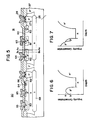
- Fig. 7 shows the profile of impurity concentration along the line B 2 -B 2 in Fig. 5.
- the collector region 62 and the emitter region 61 are formed so that the impurity concentration in the vicinity of the surface is 1/3 the maximum impurity concentration in the bulk or below, namely, b/a ⁇ 1/3 as shown in Fig. 6.
- the base region 83 which is formed simultaneously with the collector region 62 and the emitter region 61, of the LEC transistor 90 is formed, similarly to the collector region 62 and the emitter region 61 of the pnp bipolar transistor 91, so that a portion having a maximum impurity concentration is formed within the bulk, and the impurity concentration in the vicinity of the surface is lower than the maximum impurity concentration.
- portions having the maximum impurity concentrations of the collector region 62 and the emitter region 61 are formed within the bulk to form a principal current passage within the bulk instead of near the surface. Consequently, reduction in current amplification factor h FE due to surface recombination is prevented, instability in the h FE due to the condition of the interface of the oxide film is removed to provide the lateral pnp bipolar transistor 91 with a stable, high h FE .
- a high-speed device requires a high-performance lateral pnp transistor.
- the performance of the lateral pnp transistor 65 of Fig. 1 can be improved by diminishing the base width W B .
- the epitaxial concentration in general, is in the range of 5 x 10 14 to 5x 10 16 /cm 3 .
- the epitaxial concentration is not higher than 10 15 /cm 3 when the epitaxial layer 4 has a high resistance to reduce the collector junction capacity C JC so that the operating speed of the npn bipolar transistor is enhanced. Accordingly, when the base width W B of the lateral pnp transistor is diminished to a width not greater than 1.0 ⁇ m, the total quantity Q B of the impurity in the base becomes a value on the order of 10 11 /cm 2 and punch through occurs between the emitter and the collector. Thus, it is difficult to improve the performance of the lateral pnp transistor by reducing the base width W B .
- Fig. 8 shows a high-performance, stable lateral pnp bipolar transistor 93 embodying the present invention developed by solving the foregoing problems.
- the pnp transistor 93 is fabricated by a process similar to that for fabricating the lateral pnp bipolar transistor shown in Fig. 1. In-fabricating the pnp transistor 93, an embedded n-type base layer 26 is formed on a p-type silicon substrate 1, an n-type epitaxial layer 4 is formed over the embedded n-type layer 26, p-type isolation regions 37 and a field insulating layer 6 are formed, and then an n-type plug-in region 27 reaching the embedded n-type base region 27, and an n-type base contact region 28 are formed.
- a p-type collector region 62 and a p-type emitter region 61 are formed in the epitaxial layer 4 in a lateral arrangement with a spacing corresponding to the base width W B so that portions of the p-type collector region 62 and the p-type emitter region 61 respectively having maximum impurity concentrations are formed within the bulk.
- n-type region 94 having an impurity concentration higher than that of the epitaxial layer 4 and having a portion having a maximum impurity concentration is formed in an intrinsic region between the p-type collector region 62 and the p-type emitter region 61 on the same level as that on which the portions having the maximum impurity concentrations of the p-type collector region 62 and the p-type emitter region 61 are formed.
- the n-type region 94 must be formed so that the same does not overlap the collector region 62 and a p + -type emitter region 61.
- the heavily doped n-type region 94 having an impurity concentration higher than that of the epitaxial layer 4 and formed between the collector region 62 and the emitter region 61 prevents punch through attributable to the reduction in the base width W B .
- the n-type region 94 not overlapping the collector region 62 and the emitter region 61 prevents increase in junction capacity. Thus, a stable, high-performance pnp transistor can easily fabricated.
- FIG. 9A an n-type epitaxial layer 4 having an impurity concentration of 10 15 /cm 3 or below is formed over an embedded n-type base layer 26 and p-type channel stop regions 3 formed on a p-type silicon substrate 1, a field insulating layer 6 for element isolation is formed by selective oxidation, a thin SiO 2 film 7 is formed, and then an n-type base contact region 27 reaching the embedded base layer 26 is formed.
- collector openings 96 and an emitter opening 97 are formed in the thin SiO 2 film 7, and then p-type collector regions 62 and a p-type emitter region 61 are formed with a spacing corresponding to the base width W B therebetween so that portions respectively having maximum impurity concentrations are formed within the epitaxial layer 4 through the ion implantation of a p-type impurity, such as boron, by using a resist mask 100 having openings 98 and 99 of a size greater than that of the openings 96 and 97, namely, openings 98 and 99 spaced apart by a distance smaller than that between the openings 96 and 97.
- a p-type impurity such as boron
- the openings 96 and 97 in the thin SiO2 film 7 are formed simultaneously with an opening corresponding to a region including the base contact region, intrinsic base region and an active region in which an emitter region is to be formed of the npn bipolar transistor 24 (Fig. 14A).
- a polycrystalline silicon film 8 is deposited by a CVD process over the entire surface including the openings 96 and 97, the polycrystalline silicon film 8 is doped with a p-type impurity, such as boron, by ion implantation, and then the polycrystalline silicon film 8 is patterned by using a resist mask 111 to form collector contact electrodes 112 and an emitter contact electrode 113 of a p + -type polycrystalline silicon film.
- the interval l between the electrodes 112 and 113 corresponds to the base width W B , namely, the interval between the collector region 62 and the emitter region 61.
- a portion of the p + -type polycrystalline silicon film in the npn bipolar transistor 24 is patterned so that the shape of the remaining portion of the p + -type polycrystalline silicon film corresponds to the external shape of the base contact electrode (Fig. 14B).
- the epitaxial layer 4 is doped with an n-type impurity, such as arsenic, by ion implantation by using the same resist mask 111 to form a n-type region 94 having an impurity concentration on the order of 10 17 /cm 3 (a dose on the order of 10 12 /cm 2 ) in the intrinsic base regions between the collector regions 62 and the emitter region 61 so that portions respectively having maximum impurity concentrations of the doped regions are on a level the same as that on which the portions having the maximum impurity concentrations of the collector regions and the emitter region are formed.
- an n-type impurity such as arsenic
- the entire surface is coated with a SiO 2 film 10.
- the SiO 2 film 10 and the p + -type polycrystalline silicon film 8 are patterned simultaneously to form a base contact electrode 12 of p + -type polycrystalline silicon and an opening is formed to expose the active region.
- side walls are formed and boron is caused to diffuse from the collector contact electrodes 112 and the emitter contact electrode 113 formed of the p + -type polycrystalline silicon film to form heavily doped collector regions 64 and a heavily doped emitter contact region 63.
- a p + -type external base region is formed.
- a second polycrystalline silicon film is formed, the second polycrystalline silicon film is doped with a p-type impurity, such as boron, by ion implantation, the doped second polycrystalline silicon film is subjected to a heat treatment to form a p-type base region, and the second polycrystalline silicon film is doped with an n-type impurity, such as arsenic, by ion implantation to form an n-type emitter region.
- n-type impurity such as arsenic
- contact holes are formed in the insulating film consisting of the SiO 2 film 10 and the thin SiO 2 film 7, and then a collector electrode 34, base electrode 35 and an emitter electrode 36 are formed of an Al-Si alloy through a Ti/TiN film 114 in the contact holes to complete the lateral pnp bipolar transistor 93 and the npn bipolar transistor 24, not shown.
- the stable, high-performance lateral pnp transistor 93 having a reduced base width W B and the very-high-speed npn bipolar transistor 24 can be simultaneously fabricated.
- a lateral bipolar transistor in accordance with the first aspect of the present invention comprises collector regions and an emitter region each having a portion having a maximum impurity concentration formed within the substrate instead of the surface of the substrate, so that the influence of surface recombination is suppressed, a high h FE is achieved, change in surface recombination current is reduced, the h FE is uniform and stable.
- a method of fabricating a lateral bipolar transistor, in accordance with the second aspect of the present invention forms collector regions, and an emitter region in a lateral arrangement on a semiconductor substrate serving as a base region by using a first mask provided with a pair of openings, and then forms heavily doped regions connected respectively to the collector regions and the emitter regions by using a second mask provided with openings formed at an interval smaller than that between the openings of the first mask to form the base region in a base width as small as the minimum line width which can be achieved by lithography.
- a lateral bipolar transistor thus fabricated has a high f T and a high h FE .
Landscapes
- Bipolar Transistors (AREA)
- Bipolar Integrated Circuits (AREA)
- Electrodes Of Semiconductors (AREA)
Claims (4)
- Halbleiterbauteil mit einem Halbleitersubstrat (1) und einer vom Substrat (1) abgewandten Hauptfläche, wobei das Halbleiterbauteil einen lateralen Bipolartransistor mit folgendem enthält:- einem Basisbereich (26; 60) von erstem Leitungstyp;- einem Emitterbereich (61) und einem Kollektorbereich (62), die beide von einem zweiten, entgegengesetzten Leitungstyp sind und in einer Lateralanordnung im Basisbereich (60) liegen;- einem Emitterkontaktbereich (63) und einem Kollektorkontaktbereich (64), die beide vom zweiten Leitungstyp sind und höhere Verunreinigungskonzentration als der Emitterbereich (61) und der Kollektorbereich (62) aufweisen, die im Basisbereich (60) liegen, wobei sie an der Hauptfläche freiliegen und den Emitterbereich 61 bzw. den Kollektorbereich (62) kontaktieren;dadurch gekennzeichnet, dass- der Emitterbereich (61) und der Kollektorbereich (62) innerhalb des Basisbereichs (60) vergraben sind;- Abschnitte des Emitterbereichs (61) und des Kollektorbereichs (62), die am nächsten beieinander liegen, jeweils einen Spitzenwert der Fremdstoffkonzentration aufweisen, wobei jeweils benachbarte Fremdstoffkonzentrationen des Emitterbereichs (61) und des Kollektorbereichs (62), die näher an der Hauptfläche liegen, niedriger als der Spitzenwert der Fremdstoffkonzentration sind, wodurch ein Hauptstromkanal innerhalb des Basisbereichs (60) anstatt nahe an der Hauptfläche ausgebildet ist.
- Halbleiterbauteil nach Anspruch 1, ferner mit einem stark dotierten Bereich (94) vom ersten Leitungstyp, der in einem Abschnitt des Basisbereichs (60) zwischen den Abschnitten des Emitterbereichs (61) und des Kollektorbereichs (62), die am nächsten beieinander liegen, und in derselben Tiefe wie diese ausgebildet ist, mit einer Fremdstoffkonzentration, die über der des Basisbereichs (60) liegt, ohne Überlappung mit dem Emitterbereich (61) und dem Kollektorbereich (62), wodurch Durchschläge verhindert sind.
- Verfahren zum Herstellen des Halbleiterbauteils mit einem lateralen Bipolartransistor gemäß Anspruch 1, das folgende Schritte umfasst:- Herstellen eines ersten Bereichs (26) von erstem Leitungstyp auf einem Halbleitersubstrat (1) von zweitem Leitungstyp;- Herstellen einer Epitaxieschicht (4) vom ersten Leitungstyp mit einer vom Substrat (1) abgewandten Hauptfläche auf dem ersten Bereich und auf dem Substrat, wodurch der erste Bereich einen vergrabenen Basisbereich des lateralen Bipolartransistors bildet und die Epitaxieschicht (4) einen Basisbereich (60) des lateralen Bipolartransistors bildet;- Herstellen eines Emitterbereichs (61) und eines Kollektorbereichs (62) des lateralen Bipolartransistors, die beide vom zweiten Leitungstyp sind, durch Ionenimplantation unter Verwendung einer ersten Maske (81), die mit einem Paar Öffnungen versehen ist, die voneinander um einen ersten Abstand beabstandet sind, so dass der Emitterbereich (61) und der Kollektorbereich (62) Abschnitte mit einem Spitzenwert der Fremdstoffkonzentration aufweisen, und sie innerhalb der Epitaxieschicht (4) vergraben sind, wobei jeweils benachbarte Fremdstoffkonzentrationen des Emitterbereichs (61) und des Kollektorbereichs (62), die näher an der Hauptfläche liegen, niedriger sind als der Spitzenwert der Fremdstoffkonzentration des Emitterbereichs (61) und des Kollektorbereichs (62);- Herstellen eines Emitterkontaktbereichs (63) und eines Kollektorkontaktbereichs (64) des lateralen Bipolartransistors, die beide vom zweiten Leitungstyp sind, die höhere Fremdstoffkonzentration als der Emitterbereich (61) und der Kollektorbereich (62) in der Epitaxieschicht (4) aufweisen, und die mit dem Emitterbereich (61) bzw. dem Kollektorbereich (62) verbunden werden, wozu eine zweite Maske verwendet wird, die mit einem Paar Öffnungen versehen ist, die voneinander um einen zweiten Abstand beabstandet sind, der größer als der erste Abstand ist.
- Verfahren zum Herstellen eines Halbleiterbauteils mit dem Halbleiterbauteil mit einem lateralen Bipolartransistor nach Anspruch 1, und mit einem Transistor mit niedriger Emitterkonzentration, wobei das Verfahren folgende Schritte umfasst:- Herstellen eines ersten Bereichs (26) und eines zweiten Bereichs (68), beide von einem ersten Leitungstyp, in einem Abschnitt (66) zum Herstellen eines lateralen Bipolartransistors bzw. einem Abschnitt (67) zum Herstellen eines Transistors mit niedriger Emitterkonzentration auf einem Halbleitersubstrat (1) von zweitem, entgegengesetztem Leitungstyp;- Herstellen einer Epitaxieschicht (4) vom ersten Leitungstyp, mit einer Hauptfläche, die vom Substrat (1) abgewandt ist, auf dem ersten und zweiten Bereich (26; 68) und auf dem Substrat (1), wodurch der erste Bereich (26) einen vergrabenen Basisbereich des lateralen Bipolartransistors bildet, wobei der zweite Bereich (68) einen vergrabenen Kollektorbereich des Transistors mit niedriger Emitterkonzentration bildet, und die Epitaxieschicht (4) den Basisbereich (60) des lateralen Bipolartransistors und den Kollektorbereich des Transistors mit niedriger Emitterkonzentration bildet;- Herstellen von Isolierbereichen (37) vom zweiten Leitungstyp sowie einer Feldisolierschicht (6);- Herstellen eines Emitterbereichs (61) und eines Kollektorbereichs (62) des lateralen Bipolartransistors im Abschnitt (66) zum Herstellen des lateralen Bipolartransistors, die beide vom zweiten Leitungstyp sind, so dass der Emitterbereich (61) und der Kollektorbereich (62) Abschnitte mit einem Spitzenwert der Fremdstoffkonzentration aufweisen, und sie innerhalb der Epitaxieschicht (4) vergraben sind, wobei jeweils benachbarte Fremdstoffkonzentrationen des Emitterbereichs (61) und des Kollektorbereichs (62), die näher an der Hauptoberfläche liegen, niedriger als der Spitzenwert der Fremdstoffkonzentration im Emitterbereich (61) und im Kollektorbereich (62) sind, und gleichzeitiges Herstellen eines Basisbereichs (83) vom zweiten Leitungstyp für den Transistor mit niedriger Emitterkonzentration im Abschnitt (67) zum Herstellen des Emitters mit niedriger Emitterkonzentration durch Ionenimplantation in der Epitaxieschicht (4) unter Verwendung einer ersten Maske (81), die mit einem Paar Öffnungen versehen ist, die voneinander um einen ersten Abstand beabstandet sind, was im Abschnitt (66) zum Herstellen des lateralen Bipolartransistors erfolgt;- Herstellen eines Emitterkontaktbereichs (63) und eines Kollektorkontaktbereichs (64) des lateralen Bipolartransistors im Abschnitt (66) zum Herstellen des lateralen Bipolartransistors, mit gleichzeitigem Herstellen eines Basiskontaktbereichs (64) für den Transistor mit niedriger Emitterkonzentration im Abschnitt (67) zum Herstellen des Transistors mit niedriger Emitterkonzentration, die alle drei vom selben Leitungstyp sind und eine höhere Fremdstoffkonzentration als der Emitterbereich (61) und der Kollektorbereich (62) des lateralen Bipolartransistors sowie der Basisbereich (83) des Transistors mit niedriger Emitterkonzentration in der Epitaxieschicht (4) aufweisen und sie mit dem Emitterbereich (61) und dem Kollektorbereich (62) des lateralen Bipolartransistors bzw. dem Basisbereich (83) des Transistors mit niedriger Emitterkonzentration verbunden werden, wozu eine zweite Maske verwendet wird, die mit einem Paar Öffnungen versehen ist, was im Abschnitt (66) zum Herstellen des lateralen Bipolartransistors erfolgt, die voneinander um einen zweiten Abstand beabstandet sind, der größer als der erste Abstand ist;- gleichzeitiges Herstellen eines Emitterbereichs (85) und eines Kollektorkontaktbereichs (66) für den Transistor mit niedriger Emitterkonzentration in der Epitaxieschicht (4) im Abschnitt (67) zum Herstellen des Transistors mit niedriger Emitterkonzentration, wie auch eines Basiskontaktbereichs (28) für den lateralen Bipolartransistor im Abschnitt (68) zum Herstellen des lateralen Bipolartransistors, wobei alle drei vom ersten Leitungstyp sind.
Applications Claiming Priority (2)
| Application Number | Priority Date | Filing Date | Title |
|---|---|---|---|
| JP344269/89 | 1989-12-28 | ||
| JP1344269A JPH03203265A (ja) | 1989-12-28 | 1989-12-28 | 半導体装置 |
Publications (3)
| Publication Number | Publication Date |
|---|---|
| EP0435331A2 EP0435331A2 (de) | 1991-07-03 |
| EP0435331A3 EP0435331A3 (en) | 1993-09-22 |
| EP0435331B1 true EP0435331B1 (de) | 1997-09-24 |
Family
ID=18367931
Family Applications (1)
| Application Number | Title | Priority Date | Filing Date |
|---|---|---|---|
| EP90125702A Expired - Lifetime EP0435331B1 (de) | 1989-12-28 | 1990-12-28 | Halbleitervorrichtung mit einem lateralen Bipolartransistor und entsprechende Herstellungsverfahren |
Country Status (5)
| Country | Link |
|---|---|
| US (1) | US5163178A (de) |
| EP (1) | EP0435331B1 (de) |
| JP (1) | JPH03203265A (de) |
| KR (1) | KR100231808B1 (de) |
| DE (1) | DE69031488T2 (de) |
Families Citing this family (29)
| Publication number | Priority date | Publication date | Assignee | Title |
|---|---|---|---|---|
| EP0645821B1 (de) * | 1993-09-27 | 2001-09-26 | STMicroelectronics S.r.l. | Rauscharmer bipolarer Transistor |
| EP0646967B1 (de) * | 1993-09-27 | 1999-09-08 | STMicroelectronics S.r.l. | Geräuscharmer pnp-Transistor |
| JPH07235550A (ja) * | 1994-02-21 | 1995-09-05 | Toshiba Corp | 半導体装置及びその製造方法 |
| JPH0831841A (ja) | 1994-07-12 | 1996-02-02 | Sony Corp | 半導体装置及びその製造方法 |
| JP3528350B2 (ja) * | 1995-08-25 | 2004-05-17 | ソニー株式会社 | 半導体装置の製造方法 |
| US6750091B1 (en) * | 1996-03-01 | 2004-06-15 | Micron Technology | Diode formation method |
| KR100258436B1 (ko) * | 1996-10-11 | 2000-06-01 | 김덕중 | 상보형 쌍극성 트랜지스터 및 그 제조 방법 |
| US5763918A (en) * | 1996-10-22 | 1998-06-09 | International Business Machines Corp. | ESD structure that employs a schottky-barrier to reduce the likelihood of latch-up |
| JPH10189755A (ja) * | 1996-12-20 | 1998-07-21 | Nec Corp | 半導体装置及びその製造方法 |
| JP3287269B2 (ja) | 1997-06-02 | 2002-06-04 | 富士電機株式会社 | ダイオードとその製造方法 |
| CN1051880C (zh) * | 1997-12-08 | 2000-04-26 | 中国科学院上海冶金研究所 | 带有稳压管的双极型集成电路及其制造方法 |
| US6611044B2 (en) * | 1998-09-11 | 2003-08-26 | Koninklijke Philips Electronics N.V. | Lateral bipolar transistor and method of making same |
| US6291303B1 (en) * | 1998-12-16 | 2001-09-18 | United Microelectronics Corp. | Method for manufacturing a bipolar junction device |
| KR20000061059A (ko) * | 1999-03-23 | 2000-10-16 | 윤종용 | 매몰층을 갖는 쇼트키 다이오드 및 그 제조방법 |
| US6437421B1 (en) | 1999-12-03 | 2002-08-20 | Legerity, Inc. | Self-aligned dual-base semiconductor process and structure incorporating multiple bipolar device types |
| US6372595B1 (en) * | 1999-12-03 | 2002-04-16 | Legerity, Inc. | Lateral bipolar junction transistor with reduced parasitic current loss |
| US6914306B1 (en) * | 2000-08-25 | 2005-07-05 | Micron Technology, Inc. | Electrostatic discharge protection device |
| US6657273B2 (en) * | 2001-06-12 | 2003-12-02 | International Rectifirer Corporation | Termination for high voltage schottky diode |
| US7129558B2 (en) * | 2002-11-06 | 2006-10-31 | International Rectifier Corporation | Chip-scale schottky device |
| SE532625C2 (sv) * | 2007-04-11 | 2010-03-09 | Transic Ab | Halvledarkomponent i kiselkarbid |
| US8338906B2 (en) * | 2008-01-30 | 2012-12-25 | Taiwan Semiconductor Manufacturing Co., Ltd. | Schottky device |
| US7781859B2 (en) * | 2008-03-24 | 2010-08-24 | Taiwan Semiconductor Manufacturing Company, Ltd. | Schottky diode structures having deep wells for improving breakdown voltages |
| EP2180517A1 (de) * | 2008-10-24 | 2010-04-28 | Epcos Ag | Bipolarer PNP-Transistor mit seitlichem Kollektor und Herstellungsverfahren |
| US9184097B2 (en) * | 2009-03-12 | 2015-11-10 | System General Corporation | Semiconductor devices and formation methods thereof |
| JP2013149925A (ja) * | 2012-01-23 | 2013-08-01 | Toshiba Corp | 半導体装置及びその製造方法 |
| RU2556765C1 (ru) * | 2014-02-25 | 2015-07-20 | Федеральное государственное бюджетное образовательное учреждение высшего профессионального образования Кабардино-Балкарский государственный университет им. Х.М. Бербекова | Способ изготовления полупроводниковой структуры |
| CN107946355B (zh) * | 2017-03-02 | 2024-04-05 | 重庆中科渝芯电子有限公司 | 一种横向高压双极结型晶体管及其制造方法 |
| CN107946356B (zh) * | 2017-03-02 | 2024-04-09 | 重庆中科渝芯电子有限公司 | 一种横向高压功率双极结型晶体管及其制造方法 |
| CN112397507B (zh) * | 2020-11-16 | 2022-05-10 | 杰华特微电子股份有限公司 | 横向双扩散晶体管及其制造方法 |
Citations (2)
| Publication number | Priority date | Publication date | Assignee | Title |
|---|---|---|---|---|
| US4400712A (en) * | 1981-02-13 | 1983-08-23 | Bell Telephone Laboratories, Incorporated | Static bipolar random access memory |
| US4510676A (en) * | 1983-12-06 | 1985-04-16 | International Business Machines, Corporation | Method of fabricating a lateral PNP transistor |
Family Cites Families (4)
| Publication number | Priority date | Publication date | Assignee | Title |
|---|---|---|---|---|
| US3846821A (en) * | 1968-11-04 | 1974-11-05 | Hitachi Ltd | Lateral transistor having emitter region with portions of different impurity concentration |
| US4005452A (en) * | 1974-11-15 | 1977-01-25 | International Telephone And Telegraph Corporation | Method for providing electrical isolating material in selected regions of a semiconductive material and the product produced thereby |
| JPS5662361A (en) * | 1979-10-29 | 1981-05-28 | Hitachi Ltd | Semiconductor device |
| FR2492165A1 (fr) * | 1980-05-14 | 1982-04-16 | Thomson Csf | Dispositif de protection contre les courants de fuite dans des circuits integres |
-
1989
- 1989-12-28 JP JP1344269A patent/JPH03203265A/ja active Pending
-
1990
- 1990-12-18 KR KR1019900020870A patent/KR100231808B1/ko not_active Expired - Lifetime
- 1990-12-27 US US07/634,454 patent/US5163178A/en not_active Expired - Lifetime
- 1990-12-28 DE DE69031488T patent/DE69031488T2/de not_active Expired - Fee Related
- 1990-12-28 EP EP90125702A patent/EP0435331B1/de not_active Expired - Lifetime
Patent Citations (2)
| Publication number | Priority date | Publication date | Assignee | Title |
|---|---|---|---|---|
| US4400712A (en) * | 1981-02-13 | 1983-08-23 | Bell Telephone Laboratories, Incorporated | Static bipolar random access memory |
| US4510676A (en) * | 1983-12-06 | 1985-04-16 | International Business Machines, Corporation | Method of fabricating a lateral PNP transistor |
Also Published As
| Publication number | Publication date |
|---|---|
| DE69031488D1 (de) | 1997-10-30 |
| JPH03203265A (ja) | 1991-09-04 |
| EP0435331A2 (de) | 1991-07-03 |
| US5163178A (en) | 1992-11-10 |
| EP0435331A3 (en) | 1993-09-22 |
| KR910013576A (ko) | 1991-08-08 |
| KR100231808B1 (ko) | 1999-12-01 |
| DE69031488T2 (de) | 1998-04-16 |
Similar Documents
| Publication | Publication Date | Title |
|---|---|---|
| EP0435331B1 (de) | Halbleitervorrichtung mit einem lateralen Bipolartransistor und entsprechende Herstellungsverfahren | |
| US4062699A (en) | Method for fabricating diffusion self-aligned short channel MOS device | |
| JP2728671B2 (ja) | バイポーラトランジスタの製造方法 | |
| EP0170250B1 (de) | Bipolarer Transistor und Verfahren zu seiner Herstellung | |
| EP0021403B1 (de) | Selbstjustierende Halbleiterschaltungen | |
| US4412378A (en) | Method for manufacturing semiconductor device utilizing selective masking, etching and oxidation | |
| HK20993A (en) | Process for producing a semiconductor integrated circuit device including a misfet | |
| EP0401786B1 (de) | Verfahren zur Herstellung eines lateralen Bipolartransistors | |
| JP3213549B2 (ja) | 超自己整列バイポーラトランジスタの製造方法 | |
| EP0236687B1 (de) | Selbstausrichtender Kontakt auf einer diffundierten Zone des P-Typs | |
| US5077227A (en) | Semiconductor device and method for fabricating the same | |
| EP0193934B1 (de) | Integrierte Halbleiterschaltungsanordnung und Verfahren zu ihrer Herstellung | |
| US4873200A (en) | Method of fabricating a bipolar transistor | |
| JPH0241170B2 (de) | ||
| KR100248504B1 (ko) | 바이폴라 트랜지스터 및 그의 제조 방법 | |
| EP0034341B1 (de) | Verfahren zum Herstellen einer Halbleitervorrichtung | |
| US5747374A (en) | Methods of fabricating bipolar transistors having separately formed intrinsic base and link-up regions | |
| US5148252A (en) | Bipolar transistor | |
| JPH10335344A (ja) | 自己整合型ダブルポリシリコンバイポーラトランジスタ及びその製造方法 | |
| US5453387A (en) | Fabrication method of semiconductor device with neighboring n- and p-type regions | |
| US4609414A (en) | Emitter finger structure in a switching transistor | |
| JPH0366815B2 (de) | ||
| JP3068733B2 (ja) | 半導体装置の製造方法 | |
| JP2573303B2 (ja) | 半導体装置の製造方法 | |
| JP2794571B2 (ja) | バイポーラトランジスタの製造方法 |
Legal Events
| Date | Code | Title | Description |
|---|---|---|---|
| PUAI | Public reference made under article 153(3) epc to a published international application that has entered the european phase |
Free format text: ORIGINAL CODE: 0009012 |
|
| 17P | Request for examination filed |
Effective date: 19901228 |
|
| AK | Designated contracting states |
Kind code of ref document: A2 Designated state(s): DE FR GB |
|
| PUAL | Search report despatched |
Free format text: ORIGINAL CODE: 0009013 |
|
| AK | Designated contracting states |
Kind code of ref document: A3 Designated state(s): DE FR GB |
|
| 17Q | First examination report despatched |
Effective date: 19950727 |
|
| GRAG | Despatch of communication of intention to grant |
Free format text: ORIGINAL CODE: EPIDOS AGRA |
|
| GRAH | Despatch of communication of intention to grant a patent |
Free format text: ORIGINAL CODE: EPIDOS IGRA |
|
| GRAH | Despatch of communication of intention to grant a patent |
Free format text: ORIGINAL CODE: EPIDOS IGRA |
|
| GRAA | (expected) grant |
Free format text: ORIGINAL CODE: 0009210 |
|
| AK | Designated contracting states |
Kind code of ref document: B1 Designated state(s): DE FR GB |
|
| REF | Corresponds to: |
Ref document number: 69031488 Country of ref document: DE Date of ref document: 19971030 |
|
| ET | Fr: translation filed | ||
| PLBE | No opposition filed within time limit |
Free format text: ORIGINAL CODE: 0009261 |
|
| STAA | Information on the status of an ep patent application or granted ep patent |
Free format text: STATUS: NO OPPOSITION FILED WITHIN TIME LIMIT |
|
| 26N | No opposition filed | ||
| PGFP | Annual fee paid to national office [announced via postgrant information from national office to epo] |
Ref country code: FR Payment date: 20011212 Year of fee payment: 12 |
|
| PGFP | Annual fee paid to national office [announced via postgrant information from national office to epo] |
Ref country code: GB Payment date: 20011227 Year of fee payment: 12 |
|
| REG | Reference to a national code |
Ref country code: GB Ref legal event code: IF02 |
|
| PGFP | Annual fee paid to national office [announced via postgrant information from national office to epo] |
Ref country code: DE Payment date: 20020109 Year of fee payment: 12 |
|
| PG25 | Lapsed in a contracting state [announced via postgrant information from national office to epo] |
Ref country code: GB Free format text: LAPSE BECAUSE OF NON-PAYMENT OF DUE FEES Effective date: 20021228 |
|
| PG25 | Lapsed in a contracting state [announced via postgrant information from national office to epo] |
Ref country code: DE Free format text: LAPSE BECAUSE OF NON-PAYMENT OF DUE FEES Effective date: 20030701 |
|
| GBPC | Gb: european patent ceased through non-payment of renewal fee |
Effective date: 20021228 |
|
| PG25 | Lapsed in a contracting state [announced via postgrant information from national office to epo] |
Ref country code: FR Free format text: LAPSE BECAUSE OF NON-PAYMENT OF DUE FEES Effective date: 20030901 |
|
| REG | Reference to a national code |
Ref country code: FR Ref legal event code: ST |