EP0424964B1 - Read only memory device - Google Patents
Read only memory device Download PDFInfo
- Publication number
- EP0424964B1 EP0424964B1 EP90120599A EP90120599A EP0424964B1 EP 0424964 B1 EP0424964 B1 EP 0424964B1 EP 90120599 A EP90120599 A EP 90120599A EP 90120599 A EP90120599 A EP 90120599A EP 0424964 B1 EP0424964 B1 EP 0424964B1
- Authority
- EP
- European Patent Office
- Prior art keywords
- lines
- line
- column
- selection
- transistors
- Prior art date
- Legal status (The legal status is an assumption and is not a legal conclusion. Google has not performed a legal analysis and makes no representation as to the accuracy of the status listed.)
- Expired - Lifetime
Links
Images


Classifications
-
- H—ELECTRICITY
- H10—SEMICONDUCTOR DEVICES; ELECTRIC SOLID-STATE DEVICES NOT OTHERWISE PROVIDED FOR
- H10B—ELECTRONIC MEMORY DEVICES
- H10B20/00—Read-only memory [ROM] devices
-
- G—PHYSICS
- G11—INFORMATION STORAGE
- G11C—STATIC STORES
- G11C17/00—Read-only memories programmable only once; Semi-permanent stores, e.g. manually-replaceable information cards
- G11C17/08—Read-only memories programmable only once; Semi-permanent stores, e.g. manually-replaceable information cards using semiconductor devices, e.g. bipolar elements
- G11C17/10—Read-only memories programmable only once; Semi-permanent stores, e.g. manually-replaceable information cards using semiconductor devices, e.g. bipolar elements in which contents are determined during manufacturing by a predetermined arrangement of coupling elements, e.g. mask-programmable ROM
- G11C17/12—Read-only memories programmable only once; Semi-permanent stores, e.g. manually-replaceable information cards using semiconductor devices, e.g. bipolar elements in which contents are determined during manufacturing by a predetermined arrangement of coupling elements, e.g. mask-programmable ROM using field-effect devices
- G11C17/126—Virtual ground arrays
-
- Y—GENERAL TAGGING OF NEW TECHNOLOGICAL DEVELOPMENTS; GENERAL TAGGING OF CROSS-SECTIONAL TECHNOLOGIES SPANNING OVER SEVERAL SECTIONS OF THE IPC; TECHNICAL SUBJECTS COVERED BY FORMER USPC CROSS-REFERENCE ART COLLECTIONS [XRACs] AND DIGESTS
- Y10—TECHNICAL SUBJECTS COVERED BY FORMER USPC
- Y10S—TECHNICAL SUBJECTS COVERED BY FORMER USPC CROSS-REFERENCE ART COLLECTIONS [XRACs] AND DIGESTS
- Y10S438/00—Semiconductor device manufacturing: process
- Y10S438/981—Utilizing varying dielectric thickness
Definitions
- This invention relates to a read-only memory device adapted for reading out data programmed in a memory cell and, more particularly, to a read-only memory device having NOR type memory cells as indicated in the preamble of claim 1 and 29.
- NOR type memory cells as indicated in the preamble of claim 1 and 29.
- ROMs read-only memory devices
- a mask ROM having a NAND type cell circuit construction which has a so-called multi-gate structure provided with a gate electrode layer formed by two polysilicon layers, and a shallow groove or trench, as disclosed for example in “8M and 16M mask ROM Employing Shallow Trench” in a monthly magazine entitled “Semiconductor World", October, 1987, pages 33 to 38.
- a mask ROM having a NOR type cell circuit construction which has its source-drain region constructed by a diffusion region, as disclosed for example in "16 Mb ROM Design Using Bank Select Architecture" in 1988 Symposium on VLSL circuits, Japan Association of Applied Physics, material, VL-7, pages 85 to 86.
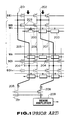
- Fig. 1 is a circuit diagram from this document showing essential portions of the mask ROM having the NOR type memory cells.
- each of the memory cells 200 arranged in a matrix configuration and adapted to be selected by word lines W 1 to W 8 is constituted by each one MOS transistor, the source-drain region of which is formed by a diffusion region which proves to be common bit lines 205, 206 and 207 for each column.
- virtual grounding lines 201 and main bit lines 202 are formed alternately, with the direction normal to the extending direction of the word lines as the longitudinal direction. These virtual grounding lines 201 and the main bit lines 202 are wired with a shift of one bit line one so as to be connected to different columns for one and the other of memory cell blocks. Thus the same bit line may be connected to the virtual grounding line 201 or to the main bit line 202 by alternative selection or bank selection of selection transistors 203 and 204.
- a given column is selected by column selection transistor 208 and a word line is selected so that data may be read out by means of the main bit line 202 and sense amplifier 209 and transmitted to an output terminal.
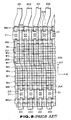
- Fig. 2 which shows the layout of the mask ROM shown in Fig. 1, the region indicated by numerous dots indicates polysilicon layers which are arrayed parallel to one another with the X-direction as the longitudinal direction.
- the region sandwitched between a pair of contact holes 211, 211 in the Y-direction represents a memory block.
- a diffusion region 213 where the contact hole 211 is formed is roughly of a pattern in the form of a letter H.
- Diffusion regions 205 to 207, ... indicate bit lines functioning as the source-drain region.
- the channel of the transistor of each cell is formed in the lower portions of the word lines W 1 to W 8 . Programming in performed by introducing impurities into the channel with the use of a mask pattern 212.
- Gate electrodes SO I , SO i+1 of a selection transistor 204 and gate electrodes SE, SE ⁇ +1 of a selection transistor 203 used for bank selection are extended parallel to the word lines W 1 to W 8 , and are arranged on both sides of the memory block.
- the memory cell driving capability is lowered when the number of serially connected transistors is increased with a view to achieving a higher degree of integration.
- the transistor channel of each cell is formed at the lower portion of the word lines W 1 to W 8 , with the channel direction being the X-direction.
- the channel region is formed between the bit lines 205 to 207, ... and the substantially H-shaped diffusion region 213, despite the fact that the gate electrodes SE, SE i- 1 , SO I and SO i+1 thereof run parallel to word lines W 1 to W 8 .
- the channel direction of these selection transistors is the Y-direction. Therefore, with the selection transistors 203, 204 for bank selection, the channel stop region need to be formed between the adjoining channels in the lower portions of the gate electrodes SE, SE i- 1, SO i and SO i+1 .
- IBM Technical Disclosure Bulletin, vol. 23, no. 6, November 1980, pages 2250-2254 discloses a scheme of a virtual grounded column line, but does not suggest divisional bit/column line scheme.
- EP-A-0011835 discloses an OR-NAND logic array which has an architecture different from the present invention and the above mentioned prior art. It uses bit lines orthogonal to word lines but there are four serially connected transistors through current path from a bit line to ground line, which does not use virtual ground architecture. Further, bank selecting architecture can not be used.
- the read-only memory device is specified in claim 1.
- a plurality of cells each including a MIS transistor having a different threshold voltage in accordance with the programmed data are arranged in a matrix configuration to form NOR type cells.
- the memory device includes word lines functioning as the gates of the MIS transistors and used in common in the cell rows and bit and column lines used as sets in the cell columns and used in common in the cells adjacent to each other in the extending direction of the word lines.
- the bit lines and the column lines are arrayed alternately in the extending direction of the word lines.
- one of the sources or the drains of the MIS transistors arrayed in each cell column is used as the bit line for data read-out while the other of the sources or the drains of the MIS transistors arrayed in each cell column is used as the column line to which a predetermined potential is applied.
- a plurality of the bit lines and a plurality of the column lines make up a group, and a plurality of such groups are provided in the memory device in its entirety. There are provided first selection means for selecting one of the groups, second selection means for selecting the bit line of the group and third selection means for selecting the column line of the group.
- the read-only memory device of the present invention is provided with the NOR type cells, the memory cell driving capability is improved.
- the bit lines and the column lines may be connected fixedly as a result of the above described arraying of the bit lines and the column lines and the provision of the first to third selection means, so that the second and the third selection means may be arrayed with a sufficient layout margin.
- MIS transistors are used as the second and the third selection means. With the channel direction of these MIS transistors being the same as the channel direction of the MIS transistors of the cells, a higher degree of integration may be achieved by the aligned formation of the selection means similar to that of the memory cells.
- the second and the third selection means are formed in a staggered relation with respect to the memory cells for facilitating the wiring for layout.
- the memory device may be divided into plural memory blocks and, in addition, a load circuit may be provided in the bit or column lines.
- NOR type memory cells are formed on the semiconductor substrate.
- an impurity region having an opposite conductivity type to that of the semiconductor substrate is formed below a plurality of parallel thick insulating films formed in striped pattern on the semiconductor substrate.
- a plurality of electrode layers extending substantially orthogonally to the striped pattern of the insulating films are formed on thin insulating films between the thick striped insulating films. Impurities are selectively introduced into the substrate region below the electrode layers functioning as the gates of the MIS transistors.
- the electrode layers may be either of a single-layer structure or a double-layer structure.
- the present embodiment is an example of a read-only memory (ROM) device having memory cells arrayed in a matrix, wherein source-drain regions of MOS transistors of the memory cells are bit and column lines which are arranged alternately. Impurities are selectively introduced by ion implantation into channel regions of the MOS transistors of the memory cells for programming the transistors.
- ROM read-only memory
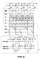
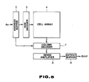
- the ROM of the present embodiment has an overall general construction as shown in Fig. 5.
- the ROM has a cell array 4 made up of a large number of memory cells in a matrix configuration and a row decoder 6 and a column decoder 7 for selecting the rows and columns in the cell array 4, respectively.
- Signals are transmitted via row decoder 6 and column decoder 7 from an address buffer 5.
- These signals from the address buffer 5 are derived from address signalsAx from outside.
- Date from the cell array 4 are amplified via column decoder 7 by a sense amplifier 8 so as to be transmitted to an output buffer 9.
- An output buffer Dour is taken out to outside from output buffer 9.
- Fig. 3 shows only a portion of a unit structure which is repeated in the extending direction of the word lines.
- the numberofthe word lines, which in Fig. 3 is four for convenience sake, is eight or more, as will be explained subsequently.
- each memory cell block 1 memory cells are arrayed in a matrix configuration.
- Each memory cell is constituted by a n-channel MOS transistor.
- the threshold value of each MOS transistor is selectively adjusted or programmed to a high threshold voltage or a low threshold voltage as a function of the programmed data.
- the gate electrodes of these MOS transistors are word lines W 1 to W 4 which are extended with the horizontal direction in the drawing as the longitudinal direction, and are shared in common by the MOS transistors of each row.
- One of the source or drain regions of the MOS transistor of each cell is the bit line B 12 , B 21 , B 22 or B 31, while the other of the source or drain regions is the column line C 11, C 12 , C 21 or C 22 .
- bit and column lines are extended with the direction normal to the word lines W 1 to W 4 as the longitudinal direction. These bit and column lines are shared in common by the MOS transistors lying along the extension of the word lines.
- bit lines B 12 , B 21, B22 and Ba1 and the column lines C 11, C 12 , C 21 and C 22 are arrayed alternately along the line of extension of the word lines in such a manner that the bit line B 12 is followed by the column line C 11, which is the followed by bit line B 21 , and so forth, with the column lines and the bit lines being arrayed alternately.
- MOS transistors T 1, T 2 , T 3 and T 4 as second selection means for alternatively connecting the bit lines B 12 , B 21 , B 22 and B 31 to the main bit lines B 1' B 2 and B 3 . That is, the bit line B 12 is connected via MOS transistor T 1 to the main bit line B 1, the bit line B 21 is connected via MOS transistor T 2 to the main bit line B 2 , the bit line B 22 is connected via MOS transistor T 3 to the main bit line B 2 and the bit line B 31 is connected via MOS transistor T 4 to the bit line B 3 .
- each main bit line is electrically connected to one of paired bit lines by the MOS transistor as the second selection means.
- Each of the MOS transistors T i and T 3 has its gate electrode as a selection line WBS, while each of the MOS transistors T 2 and T 4 has its gate electrode as a selection line WBS.
- the signals supplied to the selection line WBS and the selection line WBS are in anti phase to each other.
- the selection line WBS is at a high level
- the main bit line B 2 is connected via MOS transistor T 2 to bit line B 21 .
- the selection line WBS is at a high level
- the same main bit line B 2 is connected via MOS transistor T 3 to bit line B 22 .
- the operation for the other main bit lines is similar to that described above.
- MOS transistors T 5 , T s , T 7 , T 8 and Tg are used as switches for electrically connecting the main column lines C 1 and C 2 to column lines C 11, C 12 , C 21 and C 22 .
- the main column line C 1 is connected to column line C 11 by means of MOS transistor T s , while being connected to column line C 12 by means of MOS transistor T 7 .
- the main column line C 2 is connected to column line C 21 by means of MOS transistor T 8 , while being connected to column line C 22 by means of MOS transistor Tg. Similar electrical connections are made for the remaining main column lines.
- each of the MOS transistors T 6 and T 8 has its gate electrode as selection line WCS
- each of the MOS transistors T 5 , T 7 and T 9 has its gate electrode as selection line WCS.
- the signal supplied to selection line WCS is in antiphase with respect to the signal supplied to selection line WCS.
- MOS transistors T 6 and T 8 are turned on, so that the main column line C 1 is electrically connected to the column line C 11 , at the same time that the main column line C 2 is electrically connected to the column line C 21 .
- MOS transistors T 7 and T 9 are turned on, so that the main column line C 1 is electrically connected to the column line C 12 , at the same time that the main column line C 2 is electrically connected to the column line C 22 .
- the main bit lines B 1, B 2 and B 3 and the main column lines C 1 and C 2 are extended across the memory cell block 1 in a direction orthogonal to the word line direction.
- a load circuit 3 constructed by load transistors T 18 to T 22 .
- These load transistors T 18 to T 22 are connected to the main bit lines B 1 to B 3 and to the main column lines C 1 and C 2 , respectively.
- a source voltage Vcc is applied to these main bit lines B 1 to B 3 and to main column lines C 1 and C 2 by way of the associated load transistors T 18, T 19 , T 20, T 21 and T 22 .
- the gate electrodes of the load transistors T 18, T 19, T 20, T 21 and T 22 are connected in common and are supplied with an impedance controlling signal ⁇ 1 .
- a column selection circuit 2 selects a given row of the memory cell block on the group-by-group basis in dependence upon signals Y 1 and Y 2 from the column decoder. That is, while the main column line is selected by the signals Y 1 and Y 2 , it is the operation of the MOS transistors T 5 , T s , T 7 , T 8 or Tg as third selection means which decides to which column line the selected main column line is to be connected.
- the main bit line of the two main bit lines according to the present embodiment is selected by the signal Y 1 and Y 2 , it is the operation of the MOS transistors T 1 to T 4 as second selection means which decides to which bit line the selected main bit line is to be connected.
- the main column line is mainly selected by the signals Y 1 and Y 2 , at the same time that the main bit lines associated with the main column lines are selected.
- the main bit line may also be selected by the signals Y 1 and Y 2 .
- each group is constituted by two column lines and three bit lines.
- the cells or columns that may possibly be selected are the cells on both sides of the column lines C 11 and C 12 , such that only the cells within the group may be read out.
- Alternative selection of the bit and column lines within the group is performed by the second and third selection means.
- the main bit line B 1 is connected to a data bus line by means of a MOS transistor T 10 and another MOS transistor, not shown.
- the main bit line B 2 is connected to the data bus line by means of MOS transistors T 13 and T 14
- the main bit line B 3 is connected to the data bus line by means of the MOS transistor T 17 and another MOS transistor, not shown.
- the main column line C 1 is connected to a grounding line by means of MOS transistors T 11 and T 12
- the main column line C 2 is connected to a grounding line by means of MOS transistors T 15 and T 16 .
- the gates of the MOS transistors T 10 and T 11 are connected to an output terminal of an AND circuit 21, the gates of the MOS transistors T 12 and T 13 are connected to an output terminal of an AND circuit 22, the gates of the MOS transistors T 14 and T 15 are connected to an output terminal of an AND circuit 23 and the gates of the MOS transistors T 16 and T 17 are connected to an output terminal of an AND circuit 24.
- These AND circuits 21 to 24 are two-input gates to one of which the signals Y 1 or Y 2 are entered. To AND circuit 21 are entered the signal Y 1 and a logical product of the signals on selection lines WBS and WCS. To the AND circuit 22 are entered the signal Y 1 and a logical product of the signals on selection lines WBS and WCS.
- the signal ⁇ 1 is initially changed from the low (L) level to the high (H) level, the impedances of the load transistors T 18, T 19, T 20, T 21 and T 22 of the load circuit 3 are at predetermined levels and the main bit line B 1 , B 2 and B 3 and the main column lines C 1 and C 2 in the non-selected state are raised to the side of the source voltage Vcc.
- the operation will be explained for the case in which the memory transistors M 1 to M 7 of the first row are read out sequentially.
- the potential on the word line W 1 is raised from the “L” level to the "H” level. This selects the word line W 1 of the first row.
- the potential of the remaining word lines W 2 to W 4 is at or changed to the "L" level, thus being set to the non-selected state.
- only the signal Y 1 is raised from the "L” level to the "H” level , responsive to the signal from the column decoder, the remain signal, such as the signal Y 2 , remaining at the "L” level.
- the MOS transistors T 10 and T 11 are turned on, while the MOS transistors T 12 to T 17 , driven by the remaining AND circuits 21 to 24, remain in the off state. In this manner, MOS transistors T 10 and T 11 are turned on, with the main bit line B 1 being electrically connected to the data bus line by means of MOS transistor T 10 . Simultaneously, the main column line C 1 electrically connected to the grounding line by means of the MOS transistor T 11 for functioning as the virtual grounding line. With the main column line C 1 being thus connected to the grounding line, the potential at the main column line C 1 is lowered.
- the MOS transistors T 1 and T 3 of the second selection means are turned on and the MOS transistors T 6 and T 8 as the third selection means are turned on.
- the remaining MOS transistors T 2 , T 4 , T 5 , T 7 and T 9 of the second and third selection means remain in the off state. Since only the main bit line B 1 and the main column line C 1 are activated, as described above, the main bit line B 1 is alternatively connected to the bit line B 12 by means of the MOS transistor T 1? while the main column line C 1 is alternatively connected to the column line C 11 by means of MOS transistor T s . Of the word lines, only the word line W 1 is in the on state. Hence, only the memory transistor M 1 has been selected at this stage.
- memory transistor M 1 When the selected memory transistor M 1 has a high threshold voltage by programming by selective impurity ion implantation, memory transistor M 1 is not turned on, without the potential at the bit line B 12 not being lowered.
- the memory transistor M 1 has a low threshold voltage, the potential at the word line W 1 is turned on from the potential word line W 1 , with the potential at the main bit line B 1 being lowered.
- the potential at the main bit line B 1 is lowered, with the potential at the data bus line being also lowered.
- the potential at the data bus line is changed by the threshold voltage of the memory transistor M 1, and the output signal D out may be obtained by detecting and amplifying the potential change on the data bus line by a sense amplifier.
- the selection line WBS is changed from "L" level to "H” level.
- the output of the AND circuit 21 selected to the signal Y 1 goes low and, conversely, the output of the AND circuit 22 goes high.
- MOS transistor T 10 is turned off and the main bit line B 1 is electrically isolated from data bus line.
- the main column line C 1 is electrically connected to the grounding line by means of the MOS transistor T 12 instead of being connected via MOS transistor T 11 to the grounding line.
- the MOS transistor T 13 is turned on and the main bit line B 2 is now connected electrically to the data bus line by means of MOS transistor T 13.
- the main column line C 1 is connected to column line C 11 by means of MOS transistor T 6 . Since the selection line WBS is switched from “L" level to "H” level, MOS transistorT 2 is turned on, while MOS transistor T 3 remains off. Thus the main bit line B 2 is alternatively connected to bit line B 21 by means of MOS transistor T 2 . With the bit line B 21 and the column line C 11 selected in this manner, the memory transistor M 2 of the row pertaining to the same word line W 1 has been selected. The bit line B 21 is changed in accordance with programmed data similarly to the memory transistor M 1 and such change is demonstrated on the data bus line by way of main bit line B 2 .
- the potential at the selection line WCS is switched from "L" level to "H” level.
- the MOS transistor T 6 connected to the main bit line C 1 is turned off, while the MOS transistor T 7 is turned on, with the output of the AND circuit 22 remaining at the "H” level.
- the column line connected electrically to the main column line C 1 is changed from column line C 11 to column line C 12 , thus the memory transistor M 3 being now selected.
- the bit line B 21 is changed in accordance with programmed data similarly to the memory transistor M 1 and such change is demonstrated on the data bus line by way of main bit line B 2 .
- MOS transistor T 3 Since the potential at the signal line WBS is at "H” level, MOS transistor T 3 is also selected, such that the main signal line B 2 is connected to bit line B 22 by way of MOS transistor T 3. On the other hand, since the potential at signal line WCS is at "H” level, MOS transistor T 8 is turned on, such that column line C 21 is electrically connected to main column line C 2 . With the column line C 21 and the bit line B 22 being in use, memory transistor M 5 has been selected.
- the potentials at the selection lines WBS and WCS are changed sequentially, in the same way as when the signal Y 1 is at "H level, so that the memory transistors M s , M 7 and so forth are selected sequentially.
- the group-selecting signals Y 3, Y 4, ... proceed sequentially.
- the potential at word line W 1 is lowered, while the potential at word line W 2 is raised.
- the memory transistors are selected similarly sequentially to read out data into the data bus line.
- the ROM of the present embodiment may be divided into memory cell blocks as shown in Fig. 6. Although eight word lines are herein employed, there is not basic difference from the ROM of Fig. 3.
- the ROM shown in Fig. 6 has an number of cell blocks MB,, MB 2 , ..., MB n in a direction normal to the extending direction of the word lines.
- Each cell block MB,, MB 2 , ..., MB n has a number of lines employed permanently as alternate column lines and bit lines, and a number of memory transistors arrayed in a matrix configuration.
- MOS transistors as second control means, which are controlled by selection lines WBS.X 1 to WBS.X n , WBS.X 1 to WBS.X n, and MOS transistors, as third selection means, which are controlled by selection lines WCS.X 1 to WCS.X n, WCS.X 1 to WCS.X n.
- the column and bit lines, not shown, in the cell blocks MB,, MB 2 , ..., MB n are shortened in length in a direction normal to the extending direction of the word lines. This reduces the values of the resistances or parasitic capacitances to enable a high speed operation, while providing an advantage when the bit lines and the column lines are formed as diffusion regions.
- main bit lines B o to B m are provided in common and are formed in the same direction as that in which the bit lines are formed.
- the main column lines C 1 to C m are provided and arrayed parallel to the main bit line.
- the main bit lines B o to B m and the main column lines C 1 to C m are arrayed alternately in the extending direction of the word lines.
- a load circuit 30 is provided at the end of the cell block MB 1 in the direction normal to the extending direction of the cell block MB 1 .
- a signal ⁇ 1 for controlling the impedance of the MOS transistor constituting the load circuit 30.
- a signal ⁇ 2 may also be provided, as in an embodiment which will be explained subsequently.
- the load circuit 30 may be arranged at the end of the cell blocks in their entirety for realizing the reduced area occupied by memory cells and the high degree of integration of the memory device.
- a column selection circuit 20 is provided at the end of the cell block MB n in a direction normal to the extending direction of the word lines. Control signals WBS, WCS as well as column selection signals Y 1 to Y m from column decoder are supplied to the column selection circuit 20. By these signals, each one main column line and main bit line are selected as a group to perform the above described read-out operation. With the main bit lines B o to B m and the main column lines C 1 to C m thus used in common in the cell blocks MB 1, MB 2 , ... , MB n , the column selection circuit 20 may be arrayed at the terminal end of the cell blocks in their entirety, as in the case of the load circuit 30, for realizing reduction in the area occupied by memory cells and the high degree of integration of the memory device.
- Electrode Layer is a single
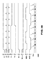
- Fig. 7 the layout for the case in which the electrode layer is formed as a single polysilicon layer is explained. Meanwhile, the layout of Fig. 5 is a partial view for simplifying the description. In practice, the layout is a continuous repetition of the pattern shown therein in the X- and Y-directions.
- a plurality of polysilicon layers shown by dotted areas are formed on the silicon substrate 41 for extending in the X-direction.
- the area between a pair of contact holes 42, 42 arrayed in the Y-direction represents one cell unit
- word lines W 1 to W 8 and selection lines WBS .X n and WCS.X n are formed as bands or stripes each formed by a polysilicon layer. These lines are spaced apart from each other by a predetermined distance and ion implantation is performed in a self-aligned manner to form channel stop regions.
- bit lines B 11, B 12 , B 21 and B 22 and column lines C 01, C o2 , C 11 and C 12 are formed with the Y-direction as the longitudinal direction, as shown by solid lines in the drawings.
- These bit lines B 11, B 12 , B 21 and B 22 and the column lines C 01, C o2 , C 11 and C 12 are of the striped patterns and are constituted by impurity diffusion regions formed at the bottom of the thick oxide film (LOCOS).
- the thick oxide film is not shown in the drawing.
- bit lines B 11 , B 12 , B 21 and B 22 and the column lines C 01, C o2 , C 11 and C 12 are formed by impurity diffusion regions formed at the lower side of the thick oxide film on the surface of the silicon substrate 41 and hence are used as the source and drain regions of the memory transistors.
- These bit lines B 11, B 12 , B 21 and B 22 and the column lines C 01, C o2 , C 11 and C 12 have characteristic terminal positions in the cell block in order that the MOS transistors and the memory transistors functioning as the second and third selection means may be in the same channel direction.
- the column lines C 01, C 11 are formed from the lower end of the word line W 1 as far as the lower end of the selection line WCS.X n , while the end 47 of the third selection means does not reach the lower end of the selection line WCS.X n .
- the perimeter of the contact hole 42 may be extended to an extended position on the column lines C 01 and C 11 .
- the column lines C 02 and C 12 are formed in a range extending from the lower end of the word line W 1 to the lower end of the selection line WCS ⁇ X n
- the impurity diffusion region extending from contact hole 42 with the main column lines C o and C 1 is extended in the Y-direction on a line of extension of the bit line and has a terminal point 48 extending from the contact hole 42 beyond the selection line WCS .X n .
- Into a region 49 between the column lines C o2 and C 12 and the impurity diffusion region at the lower end of the selection line WCS .X n extending from the contact hole 42 are implanted channel formation inhibiting impurities with the use of a mask pattern 43 shown by a broken line in Fig. 7.
- the selection transistor for the column lines C 01 and C 11 is the MOS transistor formed in the
- selection transistor for the column lines C o2 and C 12 is the MOS transistor formed in the selection lines WCS-X n . Since the channel direction of these MOS transistors
- channel stop regions may be easily formed in a self-aligned manner as in the case of the word lines W 1 to W 8 to reduce the area occupied by memory cells or to achieve a higher degree of integration of the memory device.
- bit lines are also formed so that the channel direction of the selection transistors in the X-direction.
- bit lines B 12 and B 22 are formed from the lower end of the word line W 8 as far as the lower end of the selection line WBS.X n, while the terminal end 45 of the second selection means does not reach the
- the perimetral portion of the contact hole 42 may be extended on the line of extensions of the bit lines B 12 and B 22 .
- the bit lines B 11 and B 21 are formed in the range extending from the lower end of the word line W 8 as far as the lower end of the selection line WBS-X n, such that the selection line
- WBS X n towards the contact hole 42 may be used as the gate of the selection MOS transistor.
- the region 60 between the bit lines B 11, B 12 and the impurity diffusion region extended from the contact hole 42 connecting to main bit lines B 1, B 2 is formed as a channel stop region with the use of the mask pattern 43.
- the impurity diffusion region is extended in the Y-direction on the lines of extension of the column lines C o2 and C 12 and has its terminal portion 46 lying across
- main bit lines B 1 and B 2 are alternatively connected to the bit lines, such that these main bit lines are
- bit lines B 11 and B 21 are connected via selection line WBS .
- WBS selection line
- X n to bit lines B 12 and B 22 .
- the channel direction is the same as the direction of the word lines W 1 to W 8 , which is advantageous for reducing the area occupied by the memory cells.
- the mask pattern 43 may be used simultaneously as mask 44 for programmed ion implantation which is designed for inhibiting channel formation in each memory transistor. This result in a more simplified operating process and reduced turn around time (TAT).
- TAT turn around time
- the main bit lines B 1 and B 2 are aluminum wiring layers extended in the Y-direction.
- the main column lines C o and C 1 are similarly aluminum wiring layers also extended in the Y-direction.
- These main bit lines B 1 and B 2 and the main column lines C o and C 1 are of a striped pattern and extended parallel to each other so as to connect to the impurity diffusion region formed on the surface of the silicon substrate 41 in the region of the contact hole 42.
- the contact hole 42 for the main bit lines B 1 and B 2 and the contact hole 42 for the main column lines C o and C 1 are formed in a staggered relation in the Y-direction of the cell block.
- the contact holes 42 are not adjacent to each other in the X-direction, which is advantageous for circuit integration.
- FIG. 8 the layout for the case in which the electrode layer is formed as the two polysilicon layers, is explained. Meanwhile, the layout shown in Fig. 8 is a continuous repetition of the pattern shown therein in the Y- and X-direction, as in the case of Fig. 7.
- the ROM of the present embodiment is of a striped pattern in which, as shown in Fig. 8, the first polysilicon electrode layer and a second polysilicon electrode layer are formed on a silicon substrate 51 in the X-direction.
- the selection lines WBS.X n, WCS.X n and WCS.X n+1 and the word lines W 2 , W 4 , W 6 and W 8 are formed from the first polysilicon layer, while the selection line WBS .X n, WCS .X n and
- WCS .X n+1 and the word lines W 1 , W 3, W 5 and W 7 are formed from the second polysilicon layer.
- the horizontal distance between the first and second polysilicon layers, functioning as the selection lines, is that formed solely by the thin interlayer insulating film, such that the polysilicon layers are arrayed with an interstice therebetween which is so narrow that the terminal portions thereof in the Y-direction overlap with each other.
- the word lines W 1 to W 8 is arrayed with a narrow interstice in the Y-direction by taking advantage of the properties of the two polysilicon layers. Ion implantation for transistor programming is performed for these word lines W 1 to W 8 using mask patterns 541 and 542. This ion implantation may be performed in self alignment which is effective for reducing the area.
- the arrangement of the word lines in explained subsequently. It is noted that the selection lines may be formed by single polysilicon layers arrayed side by side instead of the two-layered structure.
- Each cell block is arranged in a region defined between contact holes 52, 52 as viewed in the Y-direction. Since the two polysilicon layers are used as described above, the cell block width along the Y-direction is shorter than in the case of the single layer construction.
- bit lines B 11, B 12 , B 21 and B 22 and column lines are formed in striped pattern parallel to one another with the Y-direction as the longitudinal direction.
- the patterns of these bit lines B 11, B 12 , B 21 and B 22 and the column lines C 01, C o2 , C 11 and C 12 are formed by impurity diffusion regions formed at the lower end of the thick oxide film (LOCOS). This thick oxide film is not shown in the drawing.
- the bit lines B 11, B 12 , B 21 and B 22 and the column lines C 01, C o2 , C 11 and C 12 function as the source and drain regions of the memory transistors.
- the channel direction of the memory transistors of these bit lines B 11, B 12 , B 21 and B 22 and the column lines C 01, C o2 , C 11 and C 12 is the same as that of the MOS transistors functioning as the second and third selection means.
- the column lines C 01, C o2 , C 11 and C 12 are formed by patterns beginning at the lower end of the word line W 1 .
- the terminal ends 57 of the column lines C 01 and C 11 extend to the lower end of the selection line
- the column lines C o2 and C 12 extend to the lowers end of the selection line WCS-X n .
- the impurity diffusion region, connecting to the contact hole 52, is extended over the selection line in the Y-direction on the line of extension of the bit line for functioning as one source drain region of the MOS transistor.
- the selection transistor of the column lines C 01, C 11 is the MOS transistor formed on the selection line WCS .X n
- the selection transistor of the column lines C o2 and C 12 is the MOS transistor formed on the selection line WCS.X n .
- ion implantation for inhibiting channel formation is performed into regions 591 and 592 using mask patterns 531 and 532. These mask patterns may be formed by the same process as used for programming for the lower portions of the first and second polysilicon layers. Since the channel direction of the MOS transistor formed in each of
- X n is the same as that of the memory transistor, channel stop regions can be easily formed in a self-alignment manner, as in the case of the word lines W 1 to W 8 , with a marked advantage in reduction of the area occupied by the cells or higher integration of the memory device.
- the terminal ends of the bit lines B 12 and B 22 are at the lower end of the selection line WBS.X n and the bit lines B 11 and B 21 are formed as far as the lower end of the selection line SBS .X n .
- the MOS transistor having the channel direction in the X-direction is formed in each of the selection lines WBS.X n and WBS .X n, in a manner advantageous for reducing the occupied area.
- the regions 611 and 612 between the bit lines B 12 , B 22 and the impurity diffusion regions may be formed as the channel stop regions with the use of the mask patterns 531 and 532 which are used during programming.
- the main bit lines B 1 and B 2 and the main column lines C o and C 1 are aluminum wiring layers extended in the Y-direction in the drawing.
- the main bit lines B 1 and B 2 and the main column lines C o and C 1 are formed as striped patterns running parallel to each other, in a manner advantageous for reducing the circuit size.
- These main bit lines B 1 and B 2 and the main column lines C o and C 1 connect to the impurity diffusion region formed on the surface of the silicon substrate 41 near the contact hole 52.
- the contact holes 52 for the main bit lines B 1 and B 2 and the main column lines C o and C 1 are formed in a staggered relation in the Y-direction of the cell block, so that the contact holes 52 are not arrayed in an adjacent relation in the X-direction with an advantage for circuit integration.
- Fig. 9 is a plan view showing a cell of the ROM of the present embodiment having the two polysilicon layer structure.
- the hatched line regions indicate thick oxide films formed on the surface of a p-type semiconductor substrate 101. These oxide films are each of a striped pattern and are extended in the Y-direction parallel to each other.
- Source-drain regions 107 are formed in an aligned manner below the thick oxide film 102.
- First polysilicon layers 103 as the first electrode layers and second polysilicon layers 104 as the second electrode layers are formed as parallel striped pattern extending in the X-direction which runs at right angles with the thick oxide films 102.
- the first polysilicon layers 103 are formed by parallel stripped patterns and have an interval of a width f between the adjacent patterns.
- the second polysilicon layers 104 are formed to overlie the edges of the first polysilicon layers 103 with the edges of the second layers 104 in the Y-direction overlapping with the edges of the first layers 103.
- the memory transistors are formed in a side-by-side relation in the Y-direction without any interstices therebetween for realizing the higher degree of integration of the read-only memory device.
- a substantially square pattern 105 represents a window of a program mask by ion implantation into the lower portion of the first polysilicon layer 103
- a substantially square pattern 106 represents a window of a program mask by ion implantation into the lower portion of the second polysilicon layer 104.
- These patterns 105 and 106 larger openings, being larger in width than the layers 103, 104 in the Y-direction and bridging a pair of the thick oxide film 102,102intheX-direction.
- a pair of the thick oxide films 102, 102 function as a part of the mask along with a resist mask. Excess portions in the Y-direction may be etched off by aligned etching with the first polysilicon layer to cope with the problem of mask shifting.
- a pair of the pair of thick oxide films 102,102 and the first polysilicon layer 103 function as the mask, along with the resist mask, to cope with the problem of mask shifting.
- a positive programming may be achieved despite increased dircuit integration.
- Figs. 10 and 11 are sectional views in the X-direction.
- Fig. 10 shows a section at the second polysilicon layer wherein thick oxide films 102,102 spaced apart from each other on the surface are formed on the surface of the p-type silicon substrate 101.
- n + type impurity regions 107 On the surface of the silicon substrate 101 below the oxide films are formed n + type impurity regions 107 in an aligned manner. This n + type impurity region 107 functions as the source-drain region of the memory transistor.
- the substrate surface region which is sandwitched between a thick oxide films 102, 102 is recessed by etching to form a groove 109.
- a gate oxide film 108 thinner in thickness than the oxide film 102.
- the second polysilicon layer 104 is formed continuously when seen in cross-section over the gate oxide film 108 and the thick oxide film 102 and over the gate oxide film 108 of the adjacent memory transistor.
- This polysilicon layer 104 is formed adjacent to the gate oxide film 108 in a region defined between a pair of the thick oxide films 102, 102, and is isolated sufficiently from the n + type impurity region 107 at these thick oxide films 102, 102.
- Fig. 11, which is the section of Fig. 9 taken in the X-direction is taken at the first polysilicon layer 103.
- thick oxide films 102 are formed in a spaced apart relation on the silicon substrate 101, and an n + type region 107 is formed in an aligned manner below the oxide films.
- n + type impurity region 107 functions as the source-drain region of the memory transistor.
- the silicon substrate 101 is not etched off in a region between the oxide films 102, and a gate oxide film 108 is formed directly on the substrate surface.
- the first polysilicon layer 103 is extended continuously from above the gate oxide film 108 on the substrate surface to a region on the oxide film 102 in the direction of the section and thence to a region above the gate oxide film 108 of the adjacent memory transistor.
- Figs. 12 and 13 are sectional views of Fig. 9 taken in the Y-direction.
- Fig. 12 is a sectional view taken at the thick oxide film 102.
- a thick oxide film 102 is formed on the surface of a p-type silicon substrate 101 along a linear n + type impurity region 107.
- first polysilicon layers 103 and second polysilicon layers 104 are formed alternately. The edges of the second polysilicon layers 104 overlap with the edges of the first polysilicon layers 103 with the interposition of an interlayer insulating film, not shown.
- Fig. 12 is a sectional view taken at the thick oxide film 102.
- a thick oxide film 102 is formed on the surface of a p-type silicon substrate 101 along a linear n + type impurity region 107.
- first polysilicon layers 103 and second polysilicon layers 104 are formed alternately. The edges of the second polysilicon layers 104 overlap with the edges of the first polysilicon layers 103 with the inter
- the region of the silicon substrate 101 in register with the second polysilicon layer, 104 is etched off, and the second polysilicon layer 104 is formed on a so-formed grove 109 with the interposition of a gate oxide film 108.
- the first polysilicon layer 103 is formed on a gate oxide film 108 formed on the substrate surface.
- the memory transistors are formed for each of the polysilicon layers 103, 104.
- the channel-forming region of the substrate surface differs in height between the memory transistors which are adjacent to each other in the sectional direction.
- the memorytran- sistors in the channel-forming regions of which these impurity regions 110, 111 are formed are not turned on even when selected by the word line potential being raised, so that a pair of the n + type impurity regions 107, 107 functioning as the source-drain region are not rendered electrically conductive.
- the memory transistor not provided with the p-type impurity region is rendered electrically conductive across a pair of n + type impurity regions 107, 107 functioning as the source-drain region.
- the programmed data may be read out on the basis of such difference in operation.
- the p-type impurity region 107 functioning as the source-drain region is formed below the thick oxide film 102 to enable a high degree of integration to increase the ROM capacity. Since the memory cell structure is of the NOR type, the memory transistors are arranged side by side between the common source and the common drain. Thus the memory cell driving capacity is not changed with the number of the transistors and positive and fast data read-out may be enabled with a sufficient driving capability.
- the electrode layers are formed by two polysilicon layers 103 and 104, and the second polysilicon layer 104 is formed in a region defined between the first polysilicon layers 103 parallel thereto, so that the memory transistors may be arrayed without interstices along the longitudinal direction of the thick oxide film 102 in a manner advantageous for higher integration.
- programming may be performed more reliably by providing a step difference between the lower end of the first polysilicon layer 103 and the lower end of the second polysilicon layer 104.
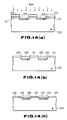
- a p-type impurity region 123 functioning as the source-drain region below a thick oxide film 124 is explained.
- an oxidation resistant layer 121 formed by a silicon nitride film is formed on a p-type substrate 120 by means of a pad oxide film.
- a resist layer 122 is applied on the oxidation resistant layer 121.
- the resist layer 122 is exposed to a pattern for formation of a thick oxide film and developed. This pattern is comprised of a parallel array of band- shaped openings formed in the memory cell array region.
- the oxidation resistant film 121 is patterned such as with the use of the RIE method. Then, as shown in Fig.
- n-type impurities such as arsenic ions
- n-type impurities are implanted to a high concentration, using the resist layer 122 and the oxidation resistant film 121 as the masks.
- n-type impurity regions 123 with the pattern of parallel stripes are formed on the surface of the silicon substrate 120.
- These n-type impurity regions 123 are formed in the same way as when forming channel stop regions in the lower portion of the usual field oxide films.
- the resist layer 122 is removed by ashing, for example, and oxidized in its entirety.
- a thick oxide film (LOCOS) 124 is formed on the surface of a region free of the oxidation resistant film 121, that is a region on which the n-type impurity region 123 is formed, as shown in Fig. 14b.
- LOC thick oxide film
- the oxidation resistant film 121 is then removed and the region on which the oxidation resistant film 121 has been formed is oxidized to form a gate oxide film 125 as shown in Fig. 14c.
- the gate oxide film 125 has a thinner thickness than that of the oxide film 124.
- Formation of electrodes or implantation of impurities for programming is then performed.
- Figs. 15a to 15c the process of forming the electrode layers and selective impurity implantation for programming is explained.
- impurity ions are selectively implanted into the lower portion of a gate oxide film 131 of a silicon substrate 130.
- Amask 132 is used for the ion implantation and impurities are implanted into a exposed substrate surface portion in register with an opening 134 formed in the mask 132.
- the implanted impurities may for example be p-type impurities, such as boron, and the opening 134 in the mask 132 is wider than the channel-forming region for the memory transistor. It is because the thick oxide film functions as a part of the mask, as described previously.
- the mask 132 is formed by, for example, a resist layer.
- the region 133 into which the impurities are implanted in this manner prove to be a channel-forming region of the transistor having a high threshold voltage.
- first polysilicon layers 135 are formed on the overall surface of the gate oxide film 131. These first polysilicon layers 135 are formed as parallel stripes extending in a direction perpendicular to the drawing sheet.
- the gate oxide film 131 in the region between the first polysilicon layers 135 is removed, portions of the silicon substrate 130 thus exposed are etched off from above to form grooves 136 aligned with the first polysilicon layers 135.
- the ends of the impurity region 133 formed to a wider width as described above are removed. With the ends of the impurity regions 133 thus etched off, it may be ensured that only the lower portion of the first polysilicon layer 135 is programmed.
- a mask 137 having an opening 138 adapted for selective implantation of impurities is formed, as shown in Fig. 15b.
- This opening 138 is a window selectively formed in the region where the second polysilicon layer is to be formed, and is of an size larger than a region below the second polysilicon layer 136 where the channel region is to be formed. It is because the previously formed first polysilicon layer 135 and the thick oxide film function as a part of the mask. By such aligned programming, sufficient data writing may be assured even when the degree of circuit integration is to be raised.
- p-type impurities such as boron
- the region 139 into which the impurities have been implanted in this manner is employed as the region for forming the transistor channel presenting a high threshold voltage.
- the mask 137 is then removed and an interlayer oxide film and a gate oxide film 140 are formed by thermal oxidation.
- the interlayer oxide film covers the surface of the first polysilicon layer 135.
- the gate oxide film 140 is formed by oxiding the side wall and bottom surfaces of the groove 136.
- a second polysilicon layer 141 is formed on the overall surface such as by the CVD method.
- the second polysilicon layer 141 is formed along the side wall and bottom surfaces of the groove 136. After formation of the second polysilicon layer 141 on the overall surface, the second polysilicon layer 141 is subjected to patterning.
- This patterning is performed in such a manner that the second polysilicon layer 141 is formed into parallel stripes such that the second polysilicon layers 141 in the stripe form overlie the grooves 136 defined between the first polysilicon layers 135 so that the edges of the second polysilicon layers 141 overlap with the edges of the first polysilicon layers 135 with the interposition of interlayer oxide films.
- a silicon oxide film (e.g. PSG) 142 as the interlayer insulating film is formed.
- an aluminum wiring layer 143 On the top of the silicon oxide film 142 is formed an aluminum wiring layer 143 in accordance with any desired pattern as shown in Fig. 15c.
- This aluminum wiring layer 143 functions as main bit lines or main column lines connected to n + type impurity region below the thick oxide film. Passivation films may be formed in accordance with the usual process to complete the read-only memory device.
- the impurity region 123 functioning as the source-drain region is formed below the thick oxide film 124, the source-drain region is not effected even when impurities for programming are introduced in alignment with the polysilicon layer. Since the two polysilicon layers are formed and the grooves 136 are formed in alignment with the first polysilicon layers 136, the openings 134, 138 of the masks 132, 137 for introducing impurities for programming may be of a wider size so that mask mismatching may be successfully coped with. A high density memory cell arraying may be assured by arranging the first polysilicon layer 135 and the second polysilicon layer 141 in a side-by-side relation and in sufficient proximity to each other with the interposition of thin interlayer oxidized films.
- the grooves 136 below the second polysilicon layers are not indispensable as long as the problem of program mask matching may be solved.
- the electrode layer need not be a polysilicon layer and may be replaced by a refractory metal silicide or polysili- cide or a refractory metal layer.
- the insulating film material need not be an oxide film but may also be a combination of the oxide film and the nitride film.
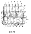
- Fig. 19 shows a layout of a portion of a column selection circuit.
- the region shown by numerous dots represent a polysilicon layer and represents signal lines 71 to which signals Y o to Y 6 from column decoder are supplied. These signal lines are extended as band in the Y-direction and arranged with an interval f 2 in the X-direction. Since the main bit line and the main column line are divided into two bit lines and two column lines respectively, the interval l 2 corresponds to twice the memory cell pitch.
- the main column lines C 1 , C 2 and C 3 and the main bit lines B 1' B 2 and B 3 are alternately formed in the Y-direction in band-like pattern as shown by hatched lines in Fig. 19.
- These main column lines C 1 to C 3 and the main bit lines B 1 to B 3 are formed by aluminum wire layers.
- a ground line 72 formed by a diffusion region is formed on the silicon substrate 70.
- This ground line 72 is extended in the Y-direction below the main bit lines B 1 to B 3 and has an extended region 73 which proves to be one source / drain region of a selection transistor Tc. That is, the selection transistor Tc has its gate electrode formed by the signal line 71 and its the other drain / source region formed by a region 74.
- the region 74 connects to the main column lines C 1 , C 2 and C 3 via contact hole 75 formed on the surface.
- the regions 74 and 73 are rendered electrically conductive by the potential of the signal line 71, while the potential of the main column lines C 1 , C 2 and C 3 is selectively set to the grounding potential .
- One extended region 73 proves to be the common source-drain of two selection transistors Tc.
- the lower region 74 of one contact hole 75 proves to be the common source-drain of two selection transistors Tc. This results in an improved circuit integration.
- a data bus line 76 formed by an Af wiring layer is formed in a pattern of extending in the X-direction.
- This data bus line 76 is electrically connected to a diffusion region 78 via contact hole 79.
- This diffusion region 78 is opposite to a diffusion region 79 with the interposition of the signal line 71.
- These diffusion regions 78 and 79 function as the source-drain region of selection transistor T B having the signal line 71 as its gate electrode.
- Each diffusion region 79 is electrically connected to the main bit lines B 1, B 2 and B 3 by means of a contact hole 80.
- the potentials or data appearing on the main bit lines B 1, B 2 and B 3 are such that only the column of the selected signal line 71 is electrically connected to the data bus line 76 and, and are outputted after amplification by the associated sense amplifier.
- the present embodiment is modified from the ROM of the first embodiment with respect to, above all, the circuit construction of the column selection circuit. Since the circuit construction is otherwise the same as the first embodiment, only the construction of the column selection circuit is hereinafter explained with reference to Fig. 16.
- the column selection circuit 2a is used for electrically connecting the data bus line and the ground line selectively to the main bit lines B 1 to B 3 or the main column lines of the memory cell block 1, and is controlled on the basis of the signal Y 1 and Y 2 .
- the main column lines C 1 and C 2 of the column selection circuit 2a of the present embodiment are directly controlled on the basis of the signals Y 1 and Y 2 . That is, the main column line C 1 is connected to the ground line by means of a MOS transistor T 35, to the gate of which the signal Y 1 is supplied. The main column line C 2 is connected to the ground line by means of a MOS transistor T 38, to the gate of which the signal Y 2 is supplied.
- the main bit lines B 1, B 2 and B 3 controlled by the signals Y 1 and Y 2 , need to be selected in accordance with the selected bit line in the same group.
- MOS transistors are provided which operate on the basis of signals over selection lines WBS, WCS, WBS and WCS.
- the main bit line B 1 is electrically connected to the data bus line by means of serially connected MOS transistors T34 and T 3o .
- the main bit line B 2 is connected to be data bus line by a first channel including serially connected MOS transistors T 36 and T 32 and a second channel including serially connected MOS transistors T 37 and T 31 .
- the main bit line B 3 is electrically connected to the data bus line by means of serially connected MOS transistors T 33 and T 39 .
- main bit lines B 1 and B 3 may also have two channels, they are not illustrated for simplicity.
- the MOS transistor T 3o , T 31 are turned on by the logical product of the signals on selection lines WBS and WCS, while the MOS transistor T 32 , T 33 are turned on by the logical sum of the signals on selection lines WBS and WCS.
- the MOS transistors T 3o , T 32 are not turned on simultaneously, while the MOS transistor T 31, T 33 are not turned on simultaneously. Therefore, when a group has been selected by the signal Y 1 and Y 2 , the main bit lines B 1 to B 3 are selected alternatively and further the operation of selecting the bit and column lines is performed for reading out data from one cell.
- the number of the transistors is significantly reduced as compared to the column selection circuit 2 of the preceding first embodiment, so that reduction in the area occupied by column selection circuit 2a may be achieved easily.
- the present embodiment is modified from the ROM of the preceding first embodiment with respect to the circuit construction of the load circuit and the column selection circuit. Since the circuit construction is otherwise the same as the preceding first embodiment, only the different circuit portions will be explained with reference to Figs. 17 and 18.
- the ROM of the present embodiment has the memory cell block 1 similar to that of the first embodiment.
- This memory cell block 1 has the main bit lines B 1, B 2 and B 3 and main column lines C 1 and C 2 extending in a direction perpendicularto the word line direction. Two bit lines and two column lines are divided out from each of these main bit lines and main column lines as in the case of the first embodiment.
- a load circuit 3a is provided at a terminal end of the memory cell block in the extending direction of the bit lines.
- This load circuit 3a has precharging MOS transistors T 41 , T 43 , T 45 , T 47 and T 49 , in addition to MOS transistors T 40 , T 42 , T 44 , T 46 and T 48 providing predetermined impedances to the main bit lines B 1 to B 3 and main column lines C 1 and C 2 .
- One source-drain regions of the MOS transistors T 40 , T 42 , T 44, T 46 and T 48 are connected to a power source line, while the other source-drain regions thereof are connected to the main bit lines or main column lines.
- a signal ⁇ 1 is supplied to the gates of these MOS transistors T 40 , T 42 T44, T 46 and T 48 .
- the one source-drain regions of the MOS transistors T 4 ,, T 43 , T 45, T 47 and T 49 are connected to the main bit or column lines and the other source-drain regions thereof are similarly connected to the power source line.
- the signal ⁇ 2 is supplied to the gate of these MOS transistors T 41, T 43 , T 47 and T 49 .
- the signal ⁇ 2 is raised to "H" level when the selected memory transistor is switched, as will be explained subsequently. Precharging is performed when the signal ⁇ 2 is raised to the "H" level.
- a column selection circuit 2b is provided at the other terminal end of the memory cell block 1 in the extending direction of the bit lines.
- MOS transistors T 50 , T 51 , T 52 and T 53 functioning as switches, are formed between the MOS transistors T 11, T 12 , T 15 and T 16 and the ground line.
- Each of these MOS transistors T 50 , T 15 , T 52 and T 53 has its gate supplied with the signal ⁇ 2 and is turned on or off when the signal ⁇ 2 is at the "H" level or at the "L” level, respectively.
- the MOS transistors T 50 , T 51, T 52 and T 53 turned off, the main column lines C 1 and C 2 disconnected from the ground level to enable effective precharging.
- the signal ⁇ 2 rises from the "L” level to the "H” level, as a result of which the MOS transistors T 41, T 43 , T 45 , T 47 and T 49 of the load circuit 3a are turned on.
- the MOS transistors T 50 , T 51, T 52 and T 53 of the column selection circuit 2b are turned off, as a result of which the potential of the main column lines C 1 and C 2 and the main bit lines B 1 to B 3 is raised to the level of the source voltage Vcc.
- the signals ⁇ 2 and ⁇ 2 are brought to the "L" level and "H” level , respectively.
- the MOS transistors T 41 , T 43 , T 45 , T 47 and T 49 are turned off and the MOS transistors T 50 , T 51 , T 52 and T 53 are turned on. This enables data to be read out so that the read-out operation is performed similarly to the first embodiment.
- high-speed data read-out may be enabled by precharging of the main bit lines and main column lines.
- bit lines and two column lines are associated with each main bit line and main column line, respectively, in the above embodiments, the present invention is not limited thereto but may be adapted to various other modifications.
Landscapes
- Semiconductor Memories (AREA)
- Read Only Memory (AREA)
Applications Claiming Priority (2)
| Application Number | Priority Date | Filing Date | Title |
|---|---|---|---|
| JP280162/89 | 1989-10-27 | ||
| JP28016289A JP2565213B2 (ja) | 1989-10-27 | 1989-10-27 | 読み出し専用メモリ装置 |
Publications (3)
| Publication Number | Publication Date |
|---|---|
| EP0424964A2 EP0424964A2 (en) | 1991-05-02 |
| EP0424964A3 EP0424964A3 (en) | 1992-11-19 |
| EP0424964B1 true EP0424964B1 (en) | 1995-12-13 |
Family
ID=17621176
Family Applications (1)
| Application Number | Title | Priority Date | Filing Date |
|---|---|---|---|
| EP90120599A Expired - Lifetime EP0424964B1 (en) | 1989-10-27 | 1990-10-26 | Read only memory device |
Country Status (5)
| Country | Link |
|---|---|
| US (3) | US5202848A (ja) |
| EP (1) | EP0424964B1 (ja) |
| JP (1) | JP2565213B2 (ja) |
| KR (1) | KR100223130B1 (ja) |
| DE (1) | DE69024173T2 (ja) |
Families Citing this family (37)
| Publication number | Priority date | Publication date | Assignee | Title |
|---|---|---|---|---|
| US5467300A (en) * | 1990-06-14 | 1995-11-14 | Creative Integrated Systems, Inc. | Grounded memory core for Roms, Eproms, and EEpproms having an address decoder, and sense amplifier |
| EP0461904A3 (en) * | 1990-06-14 | 1992-09-09 | Creative Integrated Systems, Inc. | An improved semiconductor read-only vlsi memory |
| JP3104319B2 (ja) * | 1991-08-29 | 2000-10-30 | ソニー株式会社 | 不揮発性記憶装置 |
| JPH05102436A (ja) * | 1991-10-09 | 1993-04-23 | Ricoh Co Ltd | 半導体メモリ装置とその製造方法 |
| JP2863661B2 (ja) * | 1991-12-16 | 1999-03-03 | 株式会社東芝 | 読出専用メモリ |
| US5473560A (en) * | 1992-06-29 | 1995-12-05 | Oki Electric Industry Co., Ltd. | Method of reading data and read-only memory circuit |
| JP3433808B2 (ja) * | 1992-08-05 | 2003-08-04 | 株式会社日立製作所 | 半導体集積回路装置 |
| GB9217743D0 (en) * | 1992-08-19 | 1992-09-30 | Philips Electronics Uk Ltd | A semiconductor memory device |
| JP2845414B2 (ja) * | 1992-09-18 | 1999-01-13 | シャープ株式会社 | 半導体読み出し専用メモリ |
| US5377153A (en) * | 1992-11-30 | 1994-12-27 | Sgs-Thomson Microelectronics, Inc. | Virtual ground read only memory circuit |
| JPH06318683A (ja) * | 1993-05-01 | 1994-11-15 | Toshiba Corp | 半導体記憶装置及びその製造方法 |
| US5453392A (en) * | 1993-12-02 | 1995-09-26 | United Microelectronics Corporation | Process for forming flat-cell mask ROMS |
| US5427970A (en) * | 1994-07-18 | 1995-06-27 | United Microelectronics Corporation | Method of making flash memory with high coupling ratio |
| JPH08124395A (ja) * | 1994-10-25 | 1996-05-17 | Nkk Corp | メモリ装置 |
| JP3160480B2 (ja) * | 1994-11-10 | 2001-04-25 | 株式会社東芝 | 半導体記憶装置 |
| GB2298739B (en) * | 1995-03-07 | 1999-02-17 | Hyundai Electronics Ind | Method of making a mask ROM |
| US5621697A (en) * | 1995-06-23 | 1997-04-15 | Macronix International Co., Ltd. | High density integrated circuit with bank select structure |
| TW297126B (en) * | 1995-09-13 | 1997-02-01 | Siemens Ag | Arrangement of memory cells arranged in the form of a matrix |
| JPH09107076A (ja) * | 1995-10-11 | 1997-04-22 | Nec Corp | 不揮発性半導体記憶装置 |
| JP2751892B2 (ja) * | 1995-10-11 | 1998-05-18 | 日本電気株式会社 | 半導体記憶装置 |
| JP3537010B2 (ja) * | 1995-11-28 | 2004-06-14 | シャープ株式会社 | 半導体記憶装置 |
| KR0172378B1 (ko) * | 1995-12-30 | 1999-03-30 | 김광호 | 불휘발성 반도체 메모리소자 |
| JPH09231783A (ja) * | 1996-02-26 | 1997-09-05 | Sharp Corp | 半導体記憶装置 |
| JP3380107B2 (ja) * | 1996-03-22 | 2003-02-24 | シャープ株式会社 | 半導体記憶装置 |
| JP2000124338A (ja) * | 1998-10-16 | 2000-04-28 | Sharp Corp | 半導体記憶装置 |
| US6269017B1 (en) | 1999-03-04 | 2001-07-31 | Macronix International Co., Ltd. | Multi level mask ROM with single current path |
| JP3393600B2 (ja) * | 1999-07-07 | 2003-04-07 | シャープ株式会社 | 半導体記憶装置 |
| US6175519B1 (en) | 1999-07-22 | 2001-01-16 | Macronix International Co., Ltd. | Virtual ground EPROM structure |
| US6181604B1 (en) | 1999-07-22 | 2001-01-30 | Macronix International Co., Ltd. | Method for fast programming of EPROMS and multi-level flash EPROMS |
| US6278649B1 (en) | 2000-06-30 | 2001-08-21 | Macronix International Co., Ltd. | Bank selection structures for a memory array, including a flat cell ROM array |
| KR100416599B1 (ko) * | 2001-05-31 | 2004-02-05 | 삼성전자주식회사 | 집적도와 독출동작 속도를 향상시키고 전력소모를감소시킬 수 있는 메탈 프로그래머블 롬의 메모리셀 구조 |
| JP2003060064A (ja) * | 2001-08-08 | 2003-02-28 | Sharp Corp | Mosfet、半導体装置及びその製造方法 |
| DE10224956A1 (de) * | 2002-06-05 | 2004-01-08 | Infineon Technologies Ag | Verfahren zur Einstellung der Einsatzspannung eines Feldeffekttansistors, Feldeffekttransistor sowie integrierte Schaltung |
| JP2005346755A (ja) * | 2004-05-31 | 2005-12-15 | Sharp Corp | 半導体記憶装置 |
| WO2008148091A1 (en) * | 2007-05-25 | 2008-12-04 | Marvell World Trade Ltd. | Tree type bit line decoder architecture for nor-type memory array |
| JP2011014610A (ja) * | 2009-06-30 | 2011-01-20 | Toshiba Corp | 半導体記憶装置 |
| US9685239B1 (en) * | 2016-10-12 | 2017-06-20 | Pegasus Semiconductor (Beijing) Co., Ltd | Field sub-bitline nor flash array |
Citations (3)
| Publication number | Priority date | Publication date | Assignee | Title |
|---|---|---|---|---|
| US4151020A (en) * | 1977-01-26 | 1979-04-24 | Texas Instruments Incorporated | High density N-channel silicon gate read only memory |
| US4385432A (en) * | 1978-05-18 | 1983-05-31 | Texas Instruments Incorporated | Closely-spaced double level conductors for MOS read only |
| US5051809A (en) * | 1989-06-17 | 1991-09-24 | Ricoh Company, Ltd. | Memory cell array of planar cell structure |
Family Cites Families (23)
| Publication number | Priority date | Publication date | Assignee | Title |
|---|---|---|---|---|
| US4035906A (en) * | 1975-07-23 | 1977-07-19 | Texas Instruments Incorporated | Silicon gate CCD structure |
| US4027382A (en) * | 1975-07-23 | 1977-06-07 | Texas Instruments Incorporated | Silicon gate CCD structure |
| US4290184A (en) * | 1978-03-20 | 1981-09-22 | Texas Instruments Incorporated | Method of making post-metal programmable MOS read only memory |
| US4268950A (en) * | 1978-06-05 | 1981-05-26 | Texas Instruments Incorporated | Post-metal ion implant programmable MOS read only memory |
| US4207616A (en) * | 1978-11-29 | 1980-06-10 | Teletype Corporation | Logic array having improved speed characteristics |
| US4262297A (en) * | 1978-12-19 | 1981-04-14 | The General Electric Company Limited | Semiconductor charge transfer device with multi-level polysilicon electrode and bus-line structure |
| US4288910A (en) * | 1979-04-16 | 1981-09-15 | Teletype Corporation | Method of manufacturing a semiconductor device |
| US4281397A (en) * | 1979-10-29 | 1981-07-28 | Texas Instruments Incorporated | Virtual ground MOS EPROM or ROM matrix |
| US4264930A (en) * | 1979-12-10 | 1981-04-28 | International Business Machines Corporation | Charge coupled device incorporating Laplacian thresholding with TDI array |
| US4356042A (en) * | 1980-11-07 | 1982-10-26 | Mostek Corporation | Method for fabricating a semiconductor read only memory |
| JPS5819144A (ja) * | 1981-07-24 | 1983-02-04 | Hitachi Ltd | 回転機の振動診断装置 |
| JPS5827335A (ja) * | 1981-08-11 | 1983-02-18 | Fujitsu Ltd | 半導体装置の製造方法 |
| JPS58222562A (ja) * | 1982-06-19 | 1983-12-24 | Mitsubishi Electric Corp | 半導体記憶装置 |
| US4612580A (en) * | 1984-09-14 | 1986-09-16 | Rca Corporation | TDM-input electrometer, as in a line transfer CCD imager, using a charge funnel |
| JPS62150600A (ja) * | 1985-12-25 | 1987-07-04 | Hitachi Ltd | 記憶装置 |
| JPS63102342A (ja) * | 1986-10-20 | 1988-05-07 | Mitsubishi Electric Corp | 半導体集積回路装置の配線構造 |
| JP2563803B2 (ja) * | 1986-10-27 | 1996-12-18 | セイコーエプソン株式会社 | 半導体記憶装置 |
| JP2555103B2 (ja) * | 1987-11-13 | 1996-11-20 | 株式会社日立製作所 | 半導体集積回路装置の製造方法 |
| JP2511485B2 (ja) * | 1988-01-12 | 1996-06-26 | 沖電気工業株式会社 | 半導体記憶装置 |
| IT1217403B (it) * | 1988-04-12 | 1990-03-22 | Sgs Thomson Microelectronics | Matrice di memoria a tovaglia con celle eprom sfalsate |
| FR2634318B1 (fr) * | 1988-07-13 | 1992-02-21 | Commissariat Energie Atomique | Procede de fabrication d'une cellule de memoire integree |
| US5070032A (en) * | 1989-03-15 | 1991-12-03 | Sundisk Corporation | Method of making dense flash eeprom semiconductor memory structures |
| US4968641A (en) * | 1989-06-22 | 1990-11-06 | Alexander Kalnitsky | Method for formation of an isolating oxide layer |
-
1989
- 1989-10-27 JP JP28016289A patent/JP2565213B2/ja not_active Expired - Fee Related
-
1990
- 1990-10-26 US US07/603,931 patent/US5202848A/en not_active Expired - Fee Related
- 1990-10-26 EP EP90120599A patent/EP0424964B1/en not_active Expired - Lifetime
- 1990-10-26 DE DE69024173T patent/DE69024173T2/de not_active Expired - Fee Related
- 1990-10-27 KR KR1019900017270A patent/KR100223130B1/ko not_active IP Right Cessation
-
1992
- 1992-05-21 US US07/886,737 patent/US5278089A/en not_active Expired - Fee Related
-
1994
- 1994-07-13 US US08/274,588 patent/US5401990A/en not_active Expired - Fee Related
Patent Citations (3)
| Publication number | Priority date | Publication date | Assignee | Title |
|---|---|---|---|---|
| US4151020A (en) * | 1977-01-26 | 1979-04-24 | Texas Instruments Incorporated | High density N-channel silicon gate read only memory |
| US4385432A (en) * | 1978-05-18 | 1983-05-31 | Texas Instruments Incorporated | Closely-spaced double level conductors for MOS read only |
| US5051809A (en) * | 1989-06-17 | 1991-09-24 | Ricoh Company, Ltd. | Memory cell array of planar cell structure |
Non-Patent Citations (2)
| Title |
|---|
| IBM TECHNICAL DISCLOSURE BULLETIN vol. 23, no. 6, November 1980, NEW-YORK, US page 2254; H.L. KALTER: 'High noise immunity column select/sense amplifier circuit' * |
| IBM TECHNICAL DISCLOSURE BULLETIN vol. 31, no. 5, October 1988, NEW-YORK, US pages 304 - 305; 'Method of partitioning a CMOS ROM array to enhance performance' * |
Also Published As
| Publication number | Publication date |
|---|---|
| US5401990A (en) | 1995-03-28 |
| JPH03142877A (ja) | 1991-06-18 |
| EP0424964A3 (en) | 1992-11-19 |
| DE69024173T2 (de) | 1996-10-10 |
| KR910008846A (ko) | 1991-05-31 |
| EP0424964A2 (en) | 1991-05-02 |
| US5202848A (en) | 1993-04-13 |
| US5278089A (en) | 1994-01-11 |
| JP2565213B2 (ja) | 1996-12-18 |
| DE69024173D1 (de) | 1996-01-25 |
| KR100223130B1 (ko) | 1999-10-15 |
Similar Documents
| Publication | Publication Date | Title |
|---|---|---|
| EP0424964B1 (en) | Read only memory device | |
| US5399891A (en) | Floating gate or flash EPROM transistor array having contactless source and drain diffusions | |
| US6285574B1 (en) | Symmetric segmented memory array architecture | |
| US5747849A (en) | Nonvolatile memory device having buried data lines and floating gate electrode on buried data lines | |
| US5338953A (en) | Electrically erasable and programmable semiconductor memory device with trench memory transistor and manufacturing method of the same | |
| US5681770A (en) | Process for making and programming a flash memory array | |
| US6528896B2 (en) | Scalable two transistor memory device | |
| US5053841A (en) | Nonvolatile semiconductor memory | |
| US6239500B1 (en) | Semiconductor device with common bit contact area | |
| JP3695539B2 (ja) | 超高密度交互金属仮想接地rom、ならびにその読み出し方法及びその製造方法 | |
| JPH0864699A (ja) | 不揮発性半導体記憶装置 | |
| JPH07235650A (ja) | 不揮発性半導体記憶装置 | |
| US5379254A (en) | Asymmetrical alternate metal virtual ground EPROM array | |
| EP0880144A2 (en) | Read only memory | |
| US7671399B2 (en) | Semiconductor storage device | |
| US6621733B2 (en) | Segmented bit line EEPROM page architecture | |
| KR0169510B1 (ko) | 불휘발성 반도체 기억 장치 및 그의 제조 방법 | |
| KR19980055726A (ko) | 플래쉬 메모리 소자 및 이를 이용한 프로그램, 소거 및 독출방법 | |
| US5101380A (en) | Semiconductor memory device | |
| JP2848211B2 (ja) | 不揮発性半導体記憶装置 | |
| US6307229B2 (en) | Nonvolatile semiconductor memory device structure with superimposed bit lines and short-circuit metal strips | |
| US5657274A (en) | Semiconductor memory device adapted to a high-speed operation, a low supply voltage, and the use of a multilevel cell with a plurality of threshold values as a memory cell transistor | |
| EP0521690B1 (en) | Non-volatile memory and method of manufacturing the same | |
| JPH1093057A (ja) | メモリセルアレー | |
| JP2940474B2 (ja) | 読み出し専用メモリ装置及びその製造方法 |
Legal Events
| Date | Code | Title | Description |
|---|---|---|---|
| PUAI | Public reference made under article 153(3) epc to a published international application that has entered the european phase |
Free format text: ORIGINAL CODE: 0009012 |
|
| 17P | Request for examination filed |
Effective date: 19901220 |
|
| AK | Designated contracting states |
Kind code of ref document: A2 Designated state(s): DE FR GB |
|
| PUAL | Search report despatched |
Free format text: ORIGINAL CODE: 0009013 |
|
| AK | Designated contracting states |
Kind code of ref document: A3 Designated state(s): DE FR GB |
|
| 17Q | First examination report despatched |
Effective date: 19940510 |
|
| GRAA | (expected) grant |
Free format text: ORIGINAL CODE: 0009210 |
|
| AK | Designated contracting states |
Kind code of ref document: B1 Designated state(s): DE FR GB |
|
| REF | Corresponds to: |
Ref document number: 69024173 Country of ref document: DE Date of ref document: 19960125 |
|
| ET | Fr: translation filed | ||
| PLBE | No opposition filed within time limit |
Free format text: ORIGINAL CODE: 0009261 |
|
| STAA | Information on the status of an ep patent application or granted ep patent |
Free format text: STATUS: NO OPPOSITION FILED WITHIN TIME LIMIT |
|
| 26N | No opposition filed | ||
| REG | Reference to a national code |
Ref country code: GB Ref legal event code: IF02 |
|
| PGFP | Annual fee paid to national office [announced via postgrant information from national office to epo] |
Ref country code: FR Payment date: 20031003 Year of fee payment: 14 |
|
| PGFP | Annual fee paid to national office [announced via postgrant information from national office to epo] |
Ref country code: GB Payment date: 20031022 Year of fee payment: 14 |
|
| PGFP | Annual fee paid to national office [announced via postgrant information from national office to epo] |
Ref country code: DE Payment date: 20031103 Year of fee payment: 14 |
|
| PG25 | Lapsed in a contracting state [announced via postgrant information from national office to epo] |
Ref country code: GB Free format text: LAPSE BECAUSE OF NON-PAYMENT OF DUE FEES Effective date: 20041026 |
|
| PG25 | Lapsed in a contracting state [announced via postgrant information from national office to epo] |
Ref country code: DE Free format text: LAPSE BECAUSE OF NON-PAYMENT OF DUE FEES Effective date: 20050503 |
|
| GBPC | Gb: european patent ceased through non-payment of renewal fee |
Effective date: 20041026 |
|
| PG25 | Lapsed in a contracting state [announced via postgrant information from national office to epo] |
Ref country code: FR Free format text: LAPSE BECAUSE OF NON-PAYMENT OF DUE FEES Effective date: 20050630 |
|
| REG | Reference to a national code |
Ref country code: FR Ref legal event code: ST |