US4968641A - Method for formation of an isolating oxide layer - Google Patents
Method for formation of an isolating oxide layer Download PDFInfo
- Publication number
- US4968641A US4968641A US07/370,319 US37031989A US4968641A US 4968641 A US4968641 A US 4968641A US 37031989 A US37031989 A US 37031989A US 4968641 A US4968641 A US 4968641A
- Authority
- US
- United States
- Prior art keywords
- layer
- isolating oxide
- nitridation
- silicon substrate
- locations
- Prior art date
- Legal status (The legal status is an assumption and is not a legal conclusion. Google has not performed a legal analysis and makes no representation as to the accuracy of the status listed.)
- Expired - Lifetime
Links
- 238000000034 method Methods 0.000 title claims abstract description 40
- 230000015572 biosynthetic process Effects 0.000 title claims abstract description 17
- 239000000758 substrate Substances 0.000 claims abstract description 53
- XUIMIQQOPSSXEZ-UHFFFAOYSA-N Silicon Chemical compound [Si] XUIMIQQOPSSXEZ-UHFFFAOYSA-N 0.000 claims abstract description 42
- 229910052710 silicon Inorganic materials 0.000 claims abstract description 42
- 239000010703 silicon Substances 0.000 claims abstract description 42
- 229910052581 Si3N4 Inorganic materials 0.000 claims abstract description 40
- HQVNEWCFYHHQES-UHFFFAOYSA-N silicon nitride Chemical compound N12[Si]34N5[Si]62N3[Si]51N64 HQVNEWCFYHHQES-UHFFFAOYSA-N 0.000 claims abstract description 40
- 150000004767 nitrides Chemical class 0.000 claims description 21
- VYPSYNLAJGMNEJ-UHFFFAOYSA-N Silicium dioxide Chemical compound O=[Si]=O VYPSYNLAJGMNEJ-UHFFFAOYSA-N 0.000 claims description 20
- 230000003647 oxidation Effects 0.000 claims description 17
- 238000007254 oxidation reaction Methods 0.000 claims description 17
- 238000009792 diffusion process Methods 0.000 claims description 15
- 239000012535 impurity Substances 0.000 claims description 13
- 239000011521 glass Substances 0.000 claims description 11
- 235000012239 silicon dioxide Nutrition 0.000 claims description 10
- 239000000377 silicon dioxide Substances 0.000 claims description 10
- 238000000151 deposition Methods 0.000 claims description 4
- 238000010438 heat treatment Methods 0.000 claims description 3
- 238000000059 patterning Methods 0.000 claims description 3
- QVGXLLKOCUKJST-UHFFFAOYSA-N atomic oxygen Chemical compound [O] QVGXLLKOCUKJST-UHFFFAOYSA-N 0.000 claims description 2
- 230000004888 barrier function Effects 0.000 claims description 2
- 229910052760 oxygen Inorganic materials 0.000 claims description 2
- 239000001301 oxygen Substances 0.000 claims description 2
- 230000001939 inductive effect Effects 0.000 claims 1
- 230000002401 inhibitory effect Effects 0.000 claims 1
- 238000001020 plasma etching Methods 0.000 claims 1
- 230000008719 thickening Effects 0.000 claims 1
- 241000293849 Cordylanthus Species 0.000 abstract description 7
- 238000005755 formation reaction Methods 0.000 description 13
- 230000000694 effects Effects 0.000 description 4
- 238000002513 implantation Methods 0.000 description 4
- 238000004519 manufacturing process Methods 0.000 description 4
- 239000004065 semiconductor Substances 0.000 description 3
- KRHYYFGTRYWZRS-UHFFFAOYSA-N Fluorane Chemical compound F KRHYYFGTRYWZRS-UHFFFAOYSA-N 0.000 description 2
- 238000007796 conventional method Methods 0.000 description 2
- 238000005530 etching Methods 0.000 description 2
- 230000000873 masking effect Effects 0.000 description 2
- 210000003323 beak Anatomy 0.000 description 1
- 239000006227 byproduct Substances 0.000 description 1
- 230000008021 deposition Effects 0.000 description 1
- 239000002019 doping agent Substances 0.000 description 1
- 238000001312 dry etching Methods 0.000 description 1
- 230000008030 elimination Effects 0.000 description 1
- 238000003379 elimination reaction Methods 0.000 description 1
- 230000005669 field effect Effects 0.000 description 1
- 239000000463 material Substances 0.000 description 1
- 238000012986 modification Methods 0.000 description 1
- 230000004048 modification Effects 0.000 description 1
- 230000001590 oxidative effect Effects 0.000 description 1
- 238000001039 wet etching Methods 0.000 description 1
Images


Classifications
-
- H—ELECTRICITY
- H01—ELECTRIC ELEMENTS
- H01L—SEMICONDUCTOR DEVICES NOT COVERED BY CLASS H10
- H01L21/00—Processes or apparatus adapted for the manufacture or treatment of semiconductor or solid state devices or of parts thereof
- H01L21/02—Manufacture or treatment of semiconductor devices or of parts thereof
- H01L21/04—Manufacture or treatment of semiconductor devices or of parts thereof the devices having potential barriers, e.g. a PN junction, depletion layer or carrier concentration layer
- H01L21/18—Manufacture or treatment of semiconductor devices or of parts thereof the devices having potential barriers, e.g. a PN junction, depletion layer or carrier concentration layer the devices having semiconductor bodies comprising elements of Group IV of the Periodic Table or AIIIBV compounds with or without impurities, e.g. doping materials
- H01L21/30—Treatment of semiconductor bodies using processes or apparatus not provided for in groups H01L21/20 - H01L21/26
- H01L21/31—Treatment of semiconductor bodies using processes or apparatus not provided for in groups H01L21/20 - H01L21/26 to form insulating layers thereon, e.g. for masking or by using photolithographic techniques; After treatment of these layers; Selection of materials for these layers
- H01L21/32—Treatment of semiconductor bodies using processes or apparatus not provided for in groups H01L21/20 - H01L21/26 to form insulating layers thereon, e.g. for masking or by using photolithographic techniques; After treatment of these layers; Selection of materials for these layers using masks
-
- H—ELECTRICITY
- H01—ELECTRIC ELEMENTS
- H01L—SEMICONDUCTOR DEVICES NOT COVERED BY CLASS H10
- H01L21/00—Processes or apparatus adapted for the manufacture or treatment of semiconductor or solid state devices or of parts thereof
- H01L21/70—Manufacture or treatment of devices consisting of a plurality of solid state components formed in or on a common substrate or of parts thereof; Manufacture of integrated circuit devices or of parts thereof
- H01L21/71—Manufacture of specific parts of devices defined in group H01L21/70
- H01L21/76—Making of isolation regions between components
- H01L21/762—Dielectric regions, e.g. EPIC dielectric isolation, LOCOS; Trench refilling techniques, SOI technology, use of channel stoppers
- H01L21/76202—Dielectric regions, e.g. EPIC dielectric isolation, LOCOS; Trench refilling techniques, SOI technology, use of channel stoppers using a local oxidation of silicon, e.g. LOCOS, SWAMI, SILO
- H01L21/76213—Dielectric regions, e.g. EPIC dielectric isolation, LOCOS; Trench refilling techniques, SOI technology, use of channel stoppers using a local oxidation of silicon, e.g. LOCOS, SWAMI, SILO introducing electrical inactive or active impurities in the local oxidation region, e.g. to alter LOCOS oxide growth characteristics or for additional isolation purpose
- H01L21/76216—Dielectric regions, e.g. EPIC dielectric isolation, LOCOS; Trench refilling techniques, SOI technology, use of channel stoppers using a local oxidation of silicon, e.g. LOCOS, SWAMI, SILO introducing electrical inactive or active impurities in the local oxidation region, e.g. to alter LOCOS oxide growth characteristics or for additional isolation purpose introducing electrical active impurities in the local oxidation region for the sole purpose of creating channel stoppers
-
- Y—GENERAL TAGGING OF NEW TECHNOLOGICAL DEVELOPMENTS; GENERAL TAGGING OF CROSS-SECTIONAL TECHNOLOGIES SPANNING OVER SEVERAL SECTIONS OF THE IPC; TECHNICAL SUBJECTS COVERED BY FORMER USPC CROSS-REFERENCE ART COLLECTIONS [XRACs] AND DIGESTS
- Y10—TECHNICAL SUBJECTS COVERED BY FORMER USPC
- Y10S—TECHNICAL SUBJECTS COVERED BY FORMER USPC CROSS-REFERENCE ART COLLECTIONS [XRACs] AND DIGESTS
- Y10S438/00—Semiconductor device manufacturing: process
- Y10S438/911—Differential oxidation and etching
Definitions
- This invention relates to methods for the formation of isolating oxide layers in semiconductor devices.
- a thick isolating oxide layer is conventionally grown into the surface of a silicon substrate between locations where Insulated Gate Field Effect Transistors (IGFETs) are formed to electrically isolate adjacent IGFETs from one another.
- IGFETs Insulated Gate Field Effect Transistors
- isolating oxide layers are formed by a sequence of steps known as the LOCal Oxidation of Silicon (LOCOS) process.
- LOCOS LOCal Oxidation of Silicon
- a thin oxide buffer layer is grown over the entire surface of a silicon substrate.
- a thick nitride layer is then deposited over the entire oxide buffer layer.
- the nitride layer is patterned photolithographically to create openings in the nitride layer where a thick isolating oxide is desired.
- Channel stop impurities may then be implanted through the openings, and silicon beneath the openings is thermally oxidized to grow a thick oxide into the substrate at the openings.
- the remaining portions of the nitride and buffer oxide layers are then removed, and IGFETs are formed in and on the exposed substrate surface.
- the thin buffer oxide layer is provided to relieve stresses which would otherwise be applied to the surface of the silicon substrate if the thick nitride were grown or deposited directly on the silicon surface.
- the thin buffer oxide layer also provides a convenient etch stop during photolithographic definition of the nitride layer.
- the thin buffer oxide layer permits lateral growth of the thick isolating oxide layer under the nitride layer at edges of the openings through the nitride layer. This lateral growth of the isolating oxide layer results in "bird's beak” formations which consume valuable area on the surface of the substrate which could otherwise be used for IGFET devices, thereby limiting the maximum device density.
- the "bird's beak” formations also aggravate “narrow channel effects” which degrade the performance of the IGFET devices.
- This invention seeks to reduce the problems described above with reference to conventional LOCOS processes.
- this invention seeks to provide a method for the formation of an isolating oxide layer in which the formation of "birds' beaks" is reduced.
- an anti-nitridation layer is formed on a silicon substrate at locations where isolating oxide is desired.
- the anti-nitridation layer has openings therethrough which expose the silicon substrate at locations where isolating oxide is not desired.
- a thin silicon nitride layer is selectively grown at the locations where isolating oxide is not desired by nitridation of the exposed silicon substrate. Isolating oxide is selectively grown at the locations where isolating oxide is desired.
- the thin silicon nitride layer inhibits oxide growth at the locations where isolating oxide is not desired.
- the thin silicon nitride layer acts as a very effective oxidation mask during the growth of the isolating oxide layer because it is grown directly on the underlying silicon.
- the reduced lateral oxide growth is partly due to the elimination of the buffer oxide layer which is commonly used between the silicon nitride layer and the underlying silicon, and partly due to the more intimate contact of the grown silicon nitride with the underlying silicon than would be possible with a deposited silicon nitride.
- the buffer oxide layer can be eliminated in the method according to the invention because the grown silicon nitride layer is made thin enough to avoid excessive stress at the surface of the underlying silicon, and because the selective growth of the silicon nitride layer eliminates the silicon nitride patterning step which requires an etch stop in the most commonly used LOCOS method.
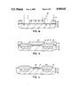
- FIGS. 1a-1c are cross-sectional views of a semiconductor device at successive stages of its manufacture by a method which includes a conventional method for the formation of an isolating oxide layer on a silicon substrate;
- FIGS. 2a-2g are cross-sectional views of a semiconductor device at successive stages of its manufacture by a method which includes a method according to an embodiment of the invention for the formation of an isolating oxide layer on a silicon substrate.
- a thin oxide buffer layer 20 is grown over the entire surface 12 of the substrate 10, and a thick nitride layer 30 is then deposited over the entire oxide buffer layer 20 and patterned photolithographically to create openings 32 in the nitride layer 30 as shown in FIG. 1a.
- the thin buffer oxide layer 20 relieves stresses which would otherwise be applied to the surface 12 of the substrate 10 if the thick nitride layer 30 were grown or deposited directly on the surface 12.
- the thin buffer oxide layer 20 also provides a convenient etch stop during photolithographic definition of the thick nitride layer 30.
- Channel stop impurities 40 may then be implanted through the openings 32 and thin buffer oxide layer 20 into the substrate 10 as shown in FIG. 1a.
- the thick nitride layer 30 acts as an implantation mask during implantation of the channel stop impurities 40.
- the silicon surface 12 beneath the openings 32 is then thermally oxidized to grow a thick oxide layer 50 into the substrate 10 at the openings 32, as shown in FIG. 1b.
- the thermal oxidation drives the channel stop impurities further into the substrate 10 to produce channel stop doped wells 42 which are also shown in FIG. 1b.
- the remaining portions of the thick nitride layer 30 and the thin buffer oxide layer 20 are removed by wet or dry etching, and IGFETs 60 are formed in and on the exposed surface 12 of the substrate 10, in resulting openings 52 in the thick isolating oxide layer 50, as shown in FIG. 1c.
- the thin buffer oxide layer 20 permits lateral growth of the thick oxide isolating layer 50 under the thick nitride layer 30 at edges 34 of the openings 32 through the thick nitride layer 30.
- This lateral growth results in "bird's beak” formations 52 which consume valuable area on the surface 12 of the substrate 10 which could otherwise be used for IGFET devices, thereby limiting the maximum device density.
- the "bird's beak” formations 52 also aggravate “narrow channel effects” which degrade the performance of the IGFET devices.
- a silicon dioxide anti-nitridation layer 120 is thermally grown over the entire surface 12 of the substrate 10, and preferentially removed at locations where an isolating oxide layer is not desired using conventional photolithographic patterning techniques.
- the silicon dioxide layer 120 remains at locations where an isolating oxide layer is desired, and has openings 122 therethrough at the locations where the isolating oxide layer is not desired.
- Exposed portions of the surface 12 of the substrate 10 are plasma etched through the openings 122 to remove traces of native oxide at the locations where an isolating oxide layer is not desired.
- a thin silicon nitride layer 130 (approximately 10 nm thick) is selectively grown at the locations where an isolating oxide layer is not desired by thermal nitridation of the portions of the surface 12 which are exposed by the openings 122.
- the silicon dioxide layer 120 is converted to an nonhomogeneous oxynitride layer 132 as a byproduct of the thermal nitridation.
- the resulting structure is shown in FIG. 2b.
- the oxynitride layer 132 is preferentially removed by etching in dilute hydrofluoric acid to expose the surface 12 of the substrate 10 at the locations where an isolating oxide layer is desired, as shown in FIG. 2c.
- a doped glass layer 140 is deposited on the exposed surface 12 of the substrate 10 and over the thin nitride layer 130 and patterned to remove the doped glass where no channel stop diffusions are required (for example in n-type device wells of CMOS circuits).
- the resulting structure is heated to diffuse channel stop impurities from the doped glass layer 140 into the substrate 10 at the locations where channel stop diffusions are desired, thereby forming doped wells 142
- the resulting structure is shown in FIG. 2c.
- the thin silicon nitride layer 130 acts as a diffusion barrier during the diffusion of the doped wells 142.
- the doped glass is removed by conventional techniques to provide the structure shown in FIG. 2e, in which the surface 12 of the substrate 10 is exposed at the locations where an isolating oxide layer is desired, and covered by the thin nitride layer 130 where no isolating oxide layer is desired.
- An isolating oxide layer 150 is then grown by oxidation of the exposed surface 12 of the silicon substrate 10 to provide the structure shown in FIG. 2f.
- the thin nitride layer 130 acts as a very effective oxidation mask during the thermal oxidation
- the channel stop impurities are driven further into the substrate 10 during the thermal oxidation to deepen the doped wells 142.
- the thin silicon nitride layer 130 is then selectively removed using conventional etching techniques, and IGFET devices are formed in and on the exposed surface 12 of the substrate 10 in resulting openings 152 in the thick isolating oxide layer 150, as shown in FIG. 2g.
- the thin silicon nitride layer 130 acts as a very effective oxidation mask during the thermal growth of the isolating oxide layer 150.
- the silicon nitride layer 130 should be made thin enough to limit the stress applied to the underlying surface 12 of the substrate 10. However, the silicon nitride layer 130 must be made thick enough to act as an effective diffusion mask during the diffusion of channel stop dopants and as an effective oxidation mask during growth of the isolating oxide layer 150. A silicon nitride layer 130 which is approximately 5 nm thick will provide adequate masking against oxidation for growth of an isolating oxide layer 150 which is approximately 3000 Angstrom units thick. A thicker silicon nitride layer 130 will be required for adequate oxidation masking during growth of a thicker isolating oxide layer 150. The silicon nitride layer 130 must be less than approximately 20 nm thick to prevent application of excessive stress to the underlying surface 12 of the substrate 10.
- the selectively grown silicon nitride layer may be thickened by selectively depositing silicon nitride on the grown silicon nitride.
- the preferential removal of the oxynitride anti-nitridation layer 132 before oxidation of the underlying silicon substrate is optional in the fabrication of NMOS circuits and other circuits where no channel stop diffusions are required because heating of the oxynitride layer 132 in an oxidizing ambient will induce oxygen to penetrate the oxynitride layer 132 to oxidize the silicon substrate 10 under the oxynitride layer 132.
- the preferential removal of the anti-nitridation layer before oxidation is required if the anti-nitridation layer is of a material which would prevent oxidation of the underlying silicon, or where the anti-nitridation layer would prevent the desired diffusion of channel stop impurities into the underlying silicon.
- the deposition, heating and removal of the doped glass layer 140 are optional and need only be used where channel stop diffusions are required. Thus, these steps may be eliminated if no channel stop diffusions are required as in the fabrication of NMOS circuits.
- the doped glass layer 140 may be patterned using conventional photolithographic techniques to provide channel stop diffusions only where required if channel stop diffusions are required only at some locations where an isolating oxide layer 150 is to be formed as in CMOS circuits.
- the thin silicon nitride layer 130 is not thick enough to be an effective implantation mask during conventional implantation of channel stop impurities.
Landscapes
- Engineering & Computer Science (AREA)
- Physics & Mathematics (AREA)
- Condensed Matter Physics & Semiconductors (AREA)
- General Physics & Mathematics (AREA)
- Manufacturing & Machinery (AREA)
- Computer Hardware Design (AREA)
- Microelectronics & Electronic Packaging (AREA)
- Power Engineering (AREA)
- Local Oxidation Of Silicon (AREA)
- Element Separation (AREA)
Abstract
Description
Claims (13)
Priority Applications (2)
| Application Number | Priority Date | Filing Date | Title |
|---|---|---|---|
| US07/370,319 US4968641A (en) | 1989-06-22 | 1989-06-22 | Method for formation of an isolating oxide layer |
| CA002008499A CA2008499C (en) | 1989-06-22 | 1990-01-24 | Method for formation of an isolating oxide layer |
Applications Claiming Priority (1)
| Application Number | Priority Date | Filing Date | Title |
|---|---|---|---|
| US07/370,319 US4968641A (en) | 1989-06-22 | 1989-06-22 | Method for formation of an isolating oxide layer |
Publications (1)
| Publication Number | Publication Date |
|---|---|
| US4968641A true US4968641A (en) | 1990-11-06 |
Family
ID=23459150
Family Applications (1)
| Application Number | Title | Priority Date | Filing Date |
|---|---|---|---|
| US07/370,319 Expired - Lifetime US4968641A (en) | 1989-06-22 | 1989-06-22 | Method for formation of an isolating oxide layer |
Country Status (2)
| Country | Link |
|---|---|
| US (1) | US4968641A (en) |
| CA (1) | CA2008499C (en) |
Cited By (10)
| Publication number | Priority date | Publication date | Assignee | Title |
|---|---|---|---|---|
| US5075245A (en) * | 1990-08-03 | 1991-12-24 | Intel Corporation | Method for improving erase characteristics of buried bit line flash EPROM devices without using sacrificial oxide growth and removal steps |
| US5278089A (en) * | 1989-10-27 | 1994-01-11 | Sony Corporation | Method for producing a read-only memory having a plurality of MISFET |
| US5654227A (en) * | 1996-01-23 | 1997-08-05 | Micron Technology, Inc. | Method for local oxidation of silicon (LOCOS) field isolation |
| US5658710A (en) * | 1993-07-16 | 1997-08-19 | Adagio Associates, Inc. | Method of making superhard mechanical microstructures |
| US5923994A (en) * | 1997-04-07 | 1999-07-13 | Oki Electric Co., Ltd. | Selective oxidation process |
| US5998277A (en) * | 1998-03-13 | 1999-12-07 | Texas Instruments - Acer Incorporated | Method to form global planarized shallow trench isolation |
| US20050142784A1 (en) * | 2003-12-30 | 2005-06-30 | Kim Dae K. | Methods of fabricating semiconductor devices |
| US20060024929A1 (en) * | 2004-07-27 | 2006-02-02 | Samsung Electronics Co., Ltd. | Method of forming a well in a substrate of a transistor of a semiconductor device |
| US8350365B1 (en) * | 2011-01-13 | 2013-01-08 | Xilinx, Inc. | Mitigation of well proximity effect in integrated circuits |
| US20190067194A1 (en) * | 2017-08-31 | 2019-02-28 | Taiwan Semiconductor Manufacturing Co., Ltd. | Interconnect structure for semiconductor device and methods of fabrication thereof |
Citations (18)
| Publication number | Priority date | Publication date | Assignee | Title |
|---|---|---|---|---|
| CA826343A (en) * | 1969-10-28 | Kooi Else | Methods of producing a semiconductor device and a semiconductor device produced by said method | |
| CA920284A (en) * | 1970-06-04 | 1973-01-30 | N.V. Philips Gloeilampenfabrieken | Method of manufacturing a semiconductor device and semiconductor device manufactured according to the method |
| US3765935A (en) * | 1971-08-10 | 1973-10-16 | Bell Telephone Labor Inc | Radiation resistant coatings for semiconductor devices |
| US3970486A (en) * | 1966-10-05 | 1976-07-20 | U.S. Philips Corporation | Methods of producing a semiconductor device and a semiconductor device produced by said method |
| US4277320A (en) * | 1979-10-01 | 1981-07-07 | Rockwell International Corporation | Process for direct thermal nitridation of silicon semiconductor devices |
| US4293588A (en) * | 1977-06-21 | 1981-10-06 | U.S. Philips Corporation | Method of manufacturing a semiconductor device using different etch rates |
| JPS58106846A (en) * | 1981-12-18 | 1983-06-25 | Nec Corp | Manufacture of semiconductor device |
| US4411929A (en) * | 1980-08-19 | 1983-10-25 | Mitsubishi Denki Kabushiki Kaisha Lsi Development Laboratory | Method for manufacturing semiconductor device |
| US4420872A (en) * | 1980-12-23 | 1983-12-20 | U.S. Philips Corporation | Method of manufacturing a semiconductor device |
| US4435447A (en) * | 1978-12-26 | 1984-03-06 | Fujitsu Limited | Method for forming an insulating film on a semiconductor substrate surface |
| US4528211A (en) * | 1983-11-04 | 1985-07-09 | General Motors Corporation | Silicon nitride formation and use in self-aligned semiconductor device manufacturing method |
| US4551910A (en) * | 1984-11-27 | 1985-11-12 | Intel Corporation | MOS Isolation processing |
| US4569117A (en) * | 1984-05-09 | 1986-02-11 | Texas Instruments Incorporated | Method of making integrated circuit with reduced narrow-width effect |
| JPS61184833A (en) * | 1985-02-12 | 1986-08-18 | Mitsubishi Electric Corp | Manufacture of semiconductor device |
| US4682408A (en) * | 1985-04-01 | 1987-07-28 | Matsushita Electronics Corporation | Method for making field oxide region with self-aligned channel stop implantation |
| US4707455A (en) * | 1986-11-26 | 1987-11-17 | General Electric Company | Method of fabricating a twin tub CMOS device |
| JPS62293728A (en) * | 1986-06-13 | 1987-12-21 | Matsushita Electric Ind Co Ltd | Manufacture of semiconductor device |
| US4740483A (en) * | 1987-03-02 | 1988-04-26 | Motorola, Inc. | Selective LPCVD tungsten deposition by nitridation of a dielectric |
-
1989
- 1989-06-22 US US07/370,319 patent/US4968641A/en not_active Expired - Lifetime
-
1990
- 1990-01-24 CA CA002008499A patent/CA2008499C/en not_active Expired - Fee Related
Patent Citations (19)
| Publication number | Priority date | Publication date | Assignee | Title |
|---|---|---|---|---|
| CA826343A (en) * | 1969-10-28 | Kooi Else | Methods of producing a semiconductor device and a semiconductor device produced by said method | |
| US3970486A (en) * | 1966-10-05 | 1976-07-20 | U.S. Philips Corporation | Methods of producing a semiconductor device and a semiconductor device produced by said method |
| CA920284A (en) * | 1970-06-04 | 1973-01-30 | N.V. Philips Gloeilampenfabrieken | Method of manufacturing a semiconductor device and semiconductor device manufactured according to the method |
| US3752711A (en) * | 1970-06-04 | 1973-08-14 | Philips Corp | Method of manufacturing an igfet and the product thereof |
| US3765935A (en) * | 1971-08-10 | 1973-10-16 | Bell Telephone Labor Inc | Radiation resistant coatings for semiconductor devices |
| US4293588A (en) * | 1977-06-21 | 1981-10-06 | U.S. Philips Corporation | Method of manufacturing a semiconductor device using different etch rates |
| US4435447A (en) * | 1978-12-26 | 1984-03-06 | Fujitsu Limited | Method for forming an insulating film on a semiconductor substrate surface |
| US4277320A (en) * | 1979-10-01 | 1981-07-07 | Rockwell International Corporation | Process for direct thermal nitridation of silicon semiconductor devices |
| US4411929A (en) * | 1980-08-19 | 1983-10-25 | Mitsubishi Denki Kabushiki Kaisha Lsi Development Laboratory | Method for manufacturing semiconductor device |
| US4420872A (en) * | 1980-12-23 | 1983-12-20 | U.S. Philips Corporation | Method of manufacturing a semiconductor device |
| JPS58106846A (en) * | 1981-12-18 | 1983-06-25 | Nec Corp | Manufacture of semiconductor device |
| US4528211A (en) * | 1983-11-04 | 1985-07-09 | General Motors Corporation | Silicon nitride formation and use in self-aligned semiconductor device manufacturing method |
| US4569117A (en) * | 1984-05-09 | 1986-02-11 | Texas Instruments Incorporated | Method of making integrated circuit with reduced narrow-width effect |
| US4551910A (en) * | 1984-11-27 | 1985-11-12 | Intel Corporation | MOS Isolation processing |
| JPS61184833A (en) * | 1985-02-12 | 1986-08-18 | Mitsubishi Electric Corp | Manufacture of semiconductor device |
| US4682408A (en) * | 1985-04-01 | 1987-07-28 | Matsushita Electronics Corporation | Method for making field oxide region with self-aligned channel stop implantation |
| JPS62293728A (en) * | 1986-06-13 | 1987-12-21 | Matsushita Electric Ind Co Ltd | Manufacture of semiconductor device |
| US4707455A (en) * | 1986-11-26 | 1987-11-17 | General Electric Company | Method of fabricating a twin tub CMOS device |
| US4740483A (en) * | 1987-03-02 | 1988-04-26 | Motorola, Inc. | Selective LPCVD tungsten deposition by nitridation of a dielectric |
Cited By (14)
| Publication number | Priority date | Publication date | Assignee | Title |
|---|---|---|---|---|
| US5278089A (en) * | 1989-10-27 | 1994-01-11 | Sony Corporation | Method for producing a read-only memory having a plurality of MISFET |
| US5075245A (en) * | 1990-08-03 | 1991-12-24 | Intel Corporation | Method for improving erase characteristics of buried bit line flash EPROM devices without using sacrificial oxide growth and removal steps |
| US5658710A (en) * | 1993-07-16 | 1997-08-19 | Adagio Associates, Inc. | Method of making superhard mechanical microstructures |
| US6090727A (en) * | 1996-01-23 | 2000-07-18 | Micron Technology, Inc. | Method for local oxidation of silicon (LOCOS) field isolation |
| US5654227A (en) * | 1996-01-23 | 1997-08-05 | Micron Technology, Inc. | Method for local oxidation of silicon (LOCOS) field isolation |
| US5923994A (en) * | 1997-04-07 | 1999-07-13 | Oki Electric Co., Ltd. | Selective oxidation process |
| US5998277A (en) * | 1998-03-13 | 1999-12-07 | Texas Instruments - Acer Incorporated | Method to form global planarized shallow trench isolation |
| US20050142784A1 (en) * | 2003-12-30 | 2005-06-30 | Kim Dae K. | Methods of fabricating semiconductor devices |
| US20060024929A1 (en) * | 2004-07-27 | 2006-02-02 | Samsung Electronics Co., Ltd. | Method of forming a well in a substrate of a transistor of a semiconductor device |
| US8350365B1 (en) * | 2011-01-13 | 2013-01-08 | Xilinx, Inc. | Mitigation of well proximity effect in integrated circuits |
| US20190067194A1 (en) * | 2017-08-31 | 2019-02-28 | Taiwan Semiconductor Manufacturing Co., Ltd. | Interconnect structure for semiconductor device and methods of fabrication thereof |
| US10515896B2 (en) * | 2017-08-31 | 2019-12-24 | Taiwan Semiconductor Manufacturing Co., Ltd. | Interconnect structure for semiconductor device and methods of fabrication thereof |
| US10777504B2 (en) | 2017-08-31 | 2020-09-15 | Taiwan Semiconductor Manufacturing Co., Ltd. | Interconnect structure for semiconductor device and methods of fabrication thereof |
| US11610841B2 (en) | 2017-08-31 | 2023-03-21 | Taiwan Semiconductor Manufacturing Co., Ltd. | Interconnect structure for semiconductor device and methods of fabrication thereof |
Also Published As
| Publication number | Publication date |
|---|---|
| CA2008499C (en) | 1993-08-17 |
| CA2008499A1 (en) | 1990-12-22 |
Similar Documents
| Publication | Publication Date | Title |
|---|---|---|
| US4459325A (en) | Semiconductor device and method for manufacturing the same | |
| US5196367A (en) | Modified field isolation process with no channel-stop implant encroachment | |
| US6027984A (en) | Method for growing oxide | |
| US4743566A (en) | Method of manufacturing a semiconductor device, in which a silicon slice is locally provided with field oxide with a channel stopper | |
| US4541167A (en) | Method for integrated circuit device isolation | |
| US5895252A (en) | Field oxidation by implanted oxygen (FIMOX) | |
| US4295266A (en) | Method of manufacturing bulk CMOS integrated circuits | |
| US4968641A (en) | Method for formation of an isolating oxide layer | |
| KR20070011408A (en) | Method of manufacturing semiconductor structure using silicon germanium | |
| US5937310A (en) | Reduced bird's beak field oxidation process using nitrogen implanted into active region | |
| KR930011500B1 (en) | Device Separation Method of Semiconductor Device | |
| JPH06163532A (en) | Semiconductor element isolation method | |
| US5397732A (en) | PBLOCOS with sandwiched thin silicon nitride layer | |
| US5139964A (en) | Method for forming isolation region of semiconductor device | |
| US5612247A (en) | Method for fabricating isolation region for a semiconductor device | |
| US5573974A (en) | Method for isolating semiconductor elements | |
| US5962914A (en) | Reduced bird's beak field oxidation process using nitrogen implanted into active region | |
| US5726091A (en) | Method of reducing bird's beak of field oxide using reoxidized nitrided pad oxide layer | |
| KR930008540B1 (en) | Isolating method in semiconductor devices | |
| KR930005237B1 (en) | Device Separation Method of Semiconductor Device | |
| JPS6390150A (en) | Manufacture of semiconductor device | |
| KR100232883B1 (en) | Method of forming an element isolation oxide film in a semiconductor device | |
| KR0167231B1 (en) | Isolation method for semiconductor device | |
| KR940001154B1 (en) | Well of cmos semiconductor device and isolation manufacturing method | |
| JP2774407B2 (en) | Method for manufacturing semiconductor device |
Legal Events
| Date | Code | Title | Description |
|---|---|---|---|
| AS | Assignment |
Owner name: NORTHERN TELECOM LIMITED, CANADA Free format text: ASSIGNMENT OF ASSIGNORS INTEREST.;ASSIGNORS:KALNITSKY, ALEXANDER;TAY, SING P.;ELLUL, JOSEPH P.;AND OTHERS;REEL/FRAME:005095/0709 Effective date: 19890605 |
|
| STCF | Information on status: patent grant |
Free format text: PATENTED CASE |
|
| FPAY | Fee payment |
Year of fee payment: 4 |
|
| FPAY | Fee payment |
Year of fee payment: 8 |
|
| AS | Assignment |
Owner name: NORTEL NETWORKS CORPORATION, CANADA Free format text: CHANGE OF NAME;ASSIGNOR:NORTHERN TELECOM LIMITED;REEL/FRAME:010567/0001 Effective date: 19990429 |
|
| AS | Assignment |
Owner name: NORTEL NETWORKS LIMITED, CANADA Free format text: CHANGE OF NAME;ASSIGNOR:NORTEL NETWORKS CORPORATION;REEL/FRAME:011195/0706 Effective date: 20000830 Owner name: NORTEL NETWORKS LIMITED,CANADA Free format text: CHANGE OF NAME;ASSIGNOR:NORTEL NETWORKS CORPORATION;REEL/FRAME:011195/0706 Effective date: 20000830 |
|
| AS | Assignment |
Owner name: STMICROELECTRONICS N.V., SWITZERLAND Free format text: ASSIGNMENT OF ASSIGNORS INTEREST;ASSIGNOR:NORTEL NETWORKS LIMITED;REEL/FRAME:011967/0805 Effective date: 20010525 |
|
| FEPP | Fee payment procedure |
Free format text: PAYOR NUMBER ASSIGNED (ORIGINAL EVENT CODE: ASPN); ENTITY STATUS OF PATENT OWNER: LARGE ENTITY |
|
| FPAY | Fee payment |
Year of fee payment: 12 |