EP0416774A1 - Procédé de traitement d'un échantillon de matériau contenant de l'aluminium - Google Patents
Procédé de traitement d'un échantillon de matériau contenant de l'aluminium Download PDFInfo
- Publication number
- EP0416774A1 EP0416774A1 EP19900309106 EP90309106A EP0416774A1 EP 0416774 A1 EP0416774 A1 EP 0416774A1 EP 19900309106 EP19900309106 EP 19900309106 EP 90309106 A EP90309106 A EP 90309106A EP 0416774 A1 EP0416774 A1 EP 0416774A1
- Authority
- EP
- European Patent Office
- Prior art keywords
- gas
- treatment
- plasma
- sample
- oxygen
- Prior art date
- Legal status (The legal status is an assumption and is not a legal conclusion. Google has not performed a legal analysis and makes no representation as to the accuracy of the status listed.)
- Granted
Links
- 229910052782 aluminium Inorganic materials 0.000 title claims abstract description 33
- 238000000034 method Methods 0.000 title claims abstract description 33
- 239000000463 material Substances 0.000 title claims abstract description 32
- XAGFODPZIPBFFR-UHFFFAOYSA-N aluminium Chemical compound [Al] XAGFODPZIPBFFR-UHFFFAOYSA-N 0.000 title claims abstract description 31
- 239000004411 aluminium Substances 0.000 title 1
- 238000011282 treatment Methods 0.000 claims abstract description 206
- 239000007789 gas Substances 0.000 claims abstract description 124
- 238000005530 etching Methods 0.000 claims abstract description 61
- QVGXLLKOCUKJST-UHFFFAOYSA-N atomic oxygen Chemical compound [O] QVGXLLKOCUKJST-UHFFFAOYSA-N 0.000 claims abstract description 51
- 239000001301 oxygen Substances 0.000 claims abstract description 50
- 229910052760 oxygen Inorganic materials 0.000 claims abstract description 50
- 229910052739 hydrogen Inorganic materials 0.000 claims abstract description 41
- 239000001257 hydrogen Substances 0.000 claims abstract description 39
- UFHFLCQGNIYNRP-UHFFFAOYSA-N Hydrogen Chemical compound [H][H] UFHFLCQGNIYNRP-UHFFFAOYSA-N 0.000 claims abstract description 33
- 229910052736 halogen Inorganic materials 0.000 claims abstract description 31
- 150000002367 halogens Chemical class 0.000 claims abstract description 31
- 238000005536 corrosion prevention Methods 0.000 claims abstract description 26
- OKKJLVBELUTLKV-UHFFFAOYSA-N Methanol Chemical compound OC OKKJLVBELUTLKV-UHFFFAOYSA-N 0.000 claims description 57
- 239000000203 mixture Substances 0.000 claims description 25
- XLYOFNOQVPJJNP-UHFFFAOYSA-N water Substances O XLYOFNOQVPJJNP-UHFFFAOYSA-N 0.000 claims description 19
- CSCPPACGZOOCGX-UHFFFAOYSA-N Acetone Chemical compound CC(C)=O CSCPPACGZOOCGX-UHFFFAOYSA-N 0.000 claims description 8
- LFQSCWFLJHTTHZ-UHFFFAOYSA-N Ethanol Chemical compound CCO LFQSCWFLJHTTHZ-UHFFFAOYSA-N 0.000 claims description 8
- 150000002431 hydrogen Chemical class 0.000 claims description 8
- 239000011261 inert gas Substances 0.000 claims description 4
- VNWKTOKETHGBQD-UHFFFAOYSA-N methane Chemical compound C VNWKTOKETHGBQD-UHFFFAOYSA-N 0.000 claims 9
- 229910052801 chlorine Inorganic materials 0.000 abstract description 20
- CPELXLSAUQHCOX-UHFFFAOYSA-N Hydrogen bromide Chemical compound Br CPELXLSAUQHCOX-UHFFFAOYSA-N 0.000 abstract description 6
- VEXZGXHMUGYJMC-UHFFFAOYSA-N Hydrochloric acid Chemical compound Cl VEXZGXHMUGYJMC-UHFFFAOYSA-N 0.000 abstract description 4
- 210000002381 plasma Anatomy 0.000 description 69
- MYMOFIZGZYHOMD-UHFFFAOYSA-N Dioxygen Chemical compound O=O MYMOFIZGZYHOMD-UHFFFAOYSA-N 0.000 description 22
- 239000000460 chlorine Substances 0.000 description 20
- ZAMOUSCENKQFHK-UHFFFAOYSA-N Chlorine atom Chemical compound [Cl] ZAMOUSCENKQFHK-UHFFFAOYSA-N 0.000 description 17
- 238000010438 heat treatment Methods 0.000 description 17
- 238000005260 corrosion Methods 0.000 description 16
- 229910001882 dioxygen Inorganic materials 0.000 description 16
- 230000007797 corrosion Effects 0.000 description 15
- 238000002336 sorption--desorption measurement Methods 0.000 description 15
- 238000004380 ashing Methods 0.000 description 14
- 238000003795 desorption Methods 0.000 description 14
- XUIMIQQOPSSXEZ-UHFFFAOYSA-N Silicon Chemical compound [Si] XUIMIQQOPSSXEZ-UHFFFAOYSA-N 0.000 description 7
- 229910052751 metal Inorganic materials 0.000 description 7
- 239000002184 metal Substances 0.000 description 7
- 229910052710 silicon Inorganic materials 0.000 description 7
- 239000010703 silicon Substances 0.000 description 7
- 238000001179 sorption measurement Methods 0.000 description 7
- 230000007423 decrease Effects 0.000 description 6
- 230000000694 effects Effects 0.000 description 6
- ATJFFYVFTNAWJD-UHFFFAOYSA-N Tin Chemical compound [Sn] ATJFFYVFTNAWJD-UHFFFAOYSA-N 0.000 description 5
- WPPDFTBPZNZZRP-UHFFFAOYSA-N aluminum copper Chemical compound [Al].[Cu] WPPDFTBPZNZZRP-UHFFFAOYSA-N 0.000 description 5
- 229910052799 carbon Inorganic materials 0.000 description 5
- 230000003247 decreasing effect Effects 0.000 description 5
- VYPSYNLAJGMNEJ-UHFFFAOYSA-N silicon dioxide Inorganic materials O=[Si]=O VYPSYNLAJGMNEJ-UHFFFAOYSA-N 0.000 description 5
- 238000009834 vaporization Methods 0.000 description 5
- 230000008016 vaporization Effects 0.000 description 5
- 229910000881 Cu alloy Inorganic materials 0.000 description 4
- 230000004888 barrier function Effects 0.000 description 4
- ILAHWRKJUDSMFH-UHFFFAOYSA-N boron tribromide Chemical compound BrB(Br)Br ILAHWRKJUDSMFH-UHFFFAOYSA-N 0.000 description 4
- 238000010586 diagram Methods 0.000 description 4
- 238000001020 plasma etching Methods 0.000 description 4
- 239000000758 substrate Substances 0.000 description 4
- VZGDMQKNWNREIO-UHFFFAOYSA-N tetrachloromethane Chemical compound ClC(Cl)(Cl)Cl VZGDMQKNWNREIO-UHFFFAOYSA-N 0.000 description 4
- 229910015844 BCl3 Inorganic materials 0.000 description 3
- OKTJSMMVPCPJKN-UHFFFAOYSA-N Carbon Chemical compound [C] OKTJSMMVPCPJKN-UHFFFAOYSA-N 0.000 description 3
- 238000006243 chemical reaction Methods 0.000 description 3
- 150000002500 ions Chemical class 0.000 description 3
- 229920002120 photoresistant polymer Polymers 0.000 description 3
- 229920006395 saturated elastomer Polymers 0.000 description 3
- TXEYQDLBPFQVAA-UHFFFAOYSA-N tetrafluoromethane Chemical compound FC(F)(F)F TXEYQDLBPFQVAA-UHFFFAOYSA-N 0.000 description 3
- FAQYAMRNWDIXMY-UHFFFAOYSA-N trichloroborane Chemical compound ClB(Cl)Cl FAQYAMRNWDIXMY-UHFFFAOYSA-N 0.000 description 3
- 229910000838 Al alloy Inorganic materials 0.000 description 2
- 229910018125 Al-Si Inorganic materials 0.000 description 2
- 229910018520 Al—Si Inorganic materials 0.000 description 2
- XKRFYHLGVUSROY-UHFFFAOYSA-N Argon Chemical compound [Ar] XKRFYHLGVUSROY-UHFFFAOYSA-N 0.000 description 2
- 229910015845 BBr3 Inorganic materials 0.000 description 2
- KZBUYRJDOAKODT-UHFFFAOYSA-N Chlorine Chemical compound ClCl KZBUYRJDOAKODT-UHFFFAOYSA-N 0.000 description 2
- OTMSDBZUPAUEDD-UHFFFAOYSA-N Ethane Chemical compound CC OTMSDBZUPAUEDD-UHFFFAOYSA-N 0.000 description 2
- 230000009471 action Effects 0.000 description 2
- 238000001704 evaporation Methods 0.000 description 2
- 230000008020 evaporation Effects 0.000 description 2
- 229910000042 hydrogen bromide Inorganic materials 0.000 description 2
- 238000004519 manufacturing process Methods 0.000 description 2
- 230000000873 masking effect Effects 0.000 description 2
- 238000009832 plasma treatment Methods 0.000 description 2
- 235000012239 silicon dioxide Nutrition 0.000 description 2
- 238000005406 washing Methods 0.000 description 2
- 229910018182 Al—Cu Inorganic materials 0.000 description 1
- 229910016006 MoSi Inorganic materials 0.000 description 1
- 229910018594 Si-Cu Inorganic materials 0.000 description 1
- 229910003910 SiCl4 Inorganic materials 0.000 description 1
- 229910008465 Si—Cu Inorganic materials 0.000 description 1
- 229910052786 argon Inorganic materials 0.000 description 1
- 230000008859 change Effects 0.000 description 1
- 229910052681 coesite Inorganic materials 0.000 description 1
- 150000001875 compounds Chemical class 0.000 description 1
- 238000007796 conventional method Methods 0.000 description 1
- 238000001816 cooling Methods 0.000 description 1
- 239000000498 cooling water Substances 0.000 description 1
- 239000010949 copper Substances 0.000 description 1
- 229910052906 cristobalite Inorganic materials 0.000 description 1
- 230000006378 damage Effects 0.000 description 1
- 230000002950 deficient Effects 0.000 description 1
- 238000009792 diffusion process Methods 0.000 description 1
- 238000004090 dissolution Methods 0.000 description 1
- 230000005684 electric field Effects 0.000 description 1
- NBVXSUQYWXRMNV-UHFFFAOYSA-N fluoromethane Chemical compound FC NBVXSUQYWXRMNV-UHFFFAOYSA-N 0.000 description 1
- 150000002366 halogen compounds Chemical class 0.000 description 1
- 239000001307 helium Substances 0.000 description 1
- 229910052734 helium Inorganic materials 0.000 description 1
- SWQJXJOGLNCZEY-UHFFFAOYSA-N helium atom Chemical compound [He] SWQJXJOGLNCZEY-UHFFFAOYSA-N 0.000 description 1
- 238000009413 insulation Methods 0.000 description 1
- 230000003993 interaction Effects 0.000 description 1
- 239000007788 liquid Substances 0.000 description 1
- 150000002739 metals Chemical class 0.000 description 1
- FAIAAWCVCHQXDN-UHFFFAOYSA-N phosphorus trichloride Chemical compound ClP(Cl)Cl FAIAAWCVCHQXDN-UHFFFAOYSA-N 0.000 description 1
- 238000001556 precipitation Methods 0.000 description 1
- 230000002265 prevention Effects 0.000 description 1
- 230000008569 process Effects 0.000 description 1
- 230000001902 propagating effect Effects 0.000 description 1
- 239000010453 quartz Substances 0.000 description 1
- 230000001603 reducing effect Effects 0.000 description 1
- 230000004044 response Effects 0.000 description 1
- 239000004065 semiconductor Substances 0.000 description 1
- 239000000377 silicon dioxide Substances 0.000 description 1
- 229910052814 silicon oxide Inorganic materials 0.000 description 1
- FDNAPBUWERUEDA-UHFFFAOYSA-N silicon tetrachloride Chemical compound Cl[Si](Cl)(Cl)Cl FDNAPBUWERUEDA-UHFFFAOYSA-N 0.000 description 1
- 238000000992 sputter etching Methods 0.000 description 1
- 229910052682 stishovite Inorganic materials 0.000 description 1
- 230000003685 thermal hair damage Effects 0.000 description 1
- 229910052905 tridymite Inorganic materials 0.000 description 1
Images

Classifications
-
- H—ELECTRICITY
- H01—ELECTRIC ELEMENTS
- H01L—SEMICONDUCTOR DEVICES NOT COVERED BY CLASS H10
- H01L21/00—Processes or apparatus adapted for the manufacture or treatment of semiconductor or solid state devices or of parts thereof
-
- H—ELECTRICITY
- H01—ELECTRIC ELEMENTS
- H01L—SEMICONDUCTOR DEVICES NOT COVERED BY CLASS H10
- H01L21/00—Processes or apparatus adapted for the manufacture or treatment of semiconductor or solid state devices or of parts thereof
- H01L21/02—Manufacture or treatment of semiconductor devices or of parts thereof
- H01L21/02041—Cleaning
- H01L21/02057—Cleaning during device manufacture
- H01L21/02068—Cleaning during device manufacture during, before or after processing of conductive layers, e.g. polysilicon or amorphous silicon layers
- H01L21/02071—Cleaning during device manufacture during, before or after processing of conductive layers, e.g. polysilicon or amorphous silicon layers the processing being a delineation, e.g. RIE, of conductive layers
-
- C—CHEMISTRY; METALLURGY
- C23—COATING METALLIC MATERIAL; COATING MATERIAL WITH METALLIC MATERIAL; CHEMICAL SURFACE TREATMENT; DIFFUSION TREATMENT OF METALLIC MATERIAL; COATING BY VACUUM EVAPORATION, BY SPUTTERING, BY ION IMPLANTATION OR BY CHEMICAL VAPOUR DEPOSITION, IN GENERAL; INHIBITING CORROSION OF METALLIC MATERIAL OR INCRUSTATION IN GENERAL
- C23F—NON-MECHANICAL REMOVAL OF METALLIC MATERIAL FROM SURFACE; INHIBITING CORROSION OF METALLIC MATERIAL OR INCRUSTATION IN GENERAL; MULTI-STEP PROCESSES FOR SURFACE TREATMENT OF METALLIC MATERIAL INVOLVING AT LEAST ONE PROCESS PROVIDED FOR IN CLASS C23 AND AT LEAST ONE PROCESS COVERED BY SUBCLASS C21D OR C22F OR CLASS C25
- C23F4/00—Processes for removing metallic material from surfaces, not provided for in group C23F1/00 or C23F3/00
-
- Y—GENERAL TAGGING OF NEW TECHNOLOGICAL DEVELOPMENTS; GENERAL TAGGING OF CROSS-SECTIONAL TECHNOLOGIES SPANNING OVER SEVERAL SECTIONS OF THE IPC; TECHNICAL SUBJECTS COVERED BY FORMER USPC CROSS-REFERENCE ART COLLECTIONS [XRACs] AND DIGESTS
- Y10—TECHNICAL SUBJECTS COVERED BY FORMER USPC
- Y10S—TECHNICAL SUBJECTS COVERED BY FORMER USPC CROSS-REFERENCE ART COLLECTIONS [XRACs] AND DIGESTS
- Y10S438/00—Semiconductor device manufacturing: process
- Y10S438/906—Cleaning of wafer as interim step
-
- Y—GENERAL TAGGING OF NEW TECHNOLOGICAL DEVELOPMENTS; GENERAL TAGGING OF CROSS-SECTIONAL TECHNOLOGIES SPANNING OVER SEVERAL SECTIONS OF THE IPC; TECHNICAL SUBJECTS COVERED BY FORMER USPC CROSS-REFERENCE ART COLLECTIONS [XRACs] AND DIGESTS
- Y10—TECHNICAL SUBJECTS COVERED BY FORMER USPC
- Y10T—TECHNICAL SUBJECTS COVERED BY FORMER US CLASSIFICATION
- Y10T428/00—Stock material or miscellaneous articles
- Y10T428/12—All metal or with adjacent metals
- Y10T428/12493—Composite; i.e., plural, adjacent, spatially distinct metal components [e.g., layers, joint, etc.]
- Y10T428/12528—Semiconductor component
-
- Y—GENERAL TAGGING OF NEW TECHNOLOGICAL DEVELOPMENTS; GENERAL TAGGING OF CROSS-SECTIONAL TECHNOLOGIES SPANNING OVER SEVERAL SECTIONS OF THE IPC; TECHNICAL SUBJECTS COVERED BY FORMER USPC CROSS-REFERENCE ART COLLECTIONS [XRACs] AND DIGESTS
- Y10—TECHNICAL SUBJECTS COVERED BY FORMER USPC
- Y10T—TECHNICAL SUBJECTS COVERED BY FORMER US CLASSIFICATION
- Y10T428/00—Stock material or miscellaneous articles
- Y10T428/12—All metal or with adjacent metals
- Y10T428/12493—Composite; i.e., plural, adjacent, spatially distinct metal components [e.g., layers, joint, etc.]
- Y10T428/12736—Al-base component
-
- Y—GENERAL TAGGING OF NEW TECHNOLOGICAL DEVELOPMENTS; GENERAL TAGGING OF CROSS-SECTIONAL TECHNOLOGIES SPANNING OVER SEVERAL SECTIONS OF THE IPC; TECHNICAL SUBJECTS COVERED BY FORMER USPC CROSS-REFERENCE ART COLLECTIONS [XRACs] AND DIGESTS
- Y10—TECHNICAL SUBJECTS COVERED BY FORMER USPC
- Y10T—TECHNICAL SUBJECTS COVERED BY FORMER US CLASSIFICATION
- Y10T428/00—Stock material or miscellaneous articles
- Y10T428/31504—Composite [nonstructural laminate]
- Y10T428/31678—Of metal
Definitions
- the present invention relates to a method of treating samples, and particularly to a method of treating samples adapted to corrosion prevention treatment of aluminum-containing wiring materials after they have been subjected to the etching treatment.
- a semiconductor wafer on which an aluminum-copper alloy film is formed is set in a reactive sputter-etching apparatus, the aluminum-copper alloy film is patterned using a plasma of such a gas as BCl3, CCl4, PCl3, BBr3 or the like, a hydrogen plasma is generated in the same apparatus, and the patterned aluminum-copper alloy film is exposed to the hydrogen plasma so as to be anti-corrosion treated.
- a plasma of such a gas as BCl3, CCl4, PCl3, BBr3 or the like a hydrogen plasma is generated in the same apparatus, and the patterned aluminum-copper alloy film is exposed to the hydrogen plasma so as to be anti-corrosion treated.
- the aluminum-containing wiring material (hereinafter referred to as "wiring film") is masked with a photoresist or the like.
- the wiring film in this case, may be aluminum-containing films (Al, Al-Si, Al-Cu, Al-Si-Cu, etc.) and laminated wiring films such as aluminum-containing film + barrier metal, cap metal, reflection-preventing film + aluminum-containing film + barrier metal.
- the barrier metal is composed of TiW, TiN or the like, and is provided between the silicon substrate and the aluminum-containing film, in order to prevent defective junction due to mutual diffusion of the silicon substrate and the aluminum-containing film and to prevent the wiring resistance from increasing due to the precipitation of silicon in the aluminum-containing film.
- the cap metal is composed of TiW, TiN, MoSi, or the like, and is used as the uppermost layer of the wiring film of a laminated structure, or is used as the reflection-preventing film.
- the reflection-preventing film is formed on the aluminum film to suppress the reflection of light at the time of exposure, so that there is formed a resist pattern faithful to the mask.
- the etching treatment is effected to treat the wafer on which the wiring film is formed using the plasma of a single gas of the type of halogen such as BCl3, Cl2, CCl4, SiCl4, HBr, BBr3 or the like, or a mixture gas thereof.
- the etching treatment is usually the one that is called reactive ion etching. With the reactive ion etching, the wiring film is etched maintaining a pattern faithful to the mask due to the interaction of radicals and ions in the plasma of the halogen-type gas, and the wiring pattern is obtained.
- a photoresist (hereinafter referred to as "resist") which is a masking material.
- Halogen components in the plasma adhere on the surface of the resist during the etching and halogen components are implanted due to the bombardment of ions.
- the halogen components during the etching or the resist components sputtered by the bombardment of ions.
- aluminum component of the once etched wiring film adhere on the side walls again thereby to form a layer that is called side wall. This layer consists of such components as aluminum, chlorine, carbon, hydrogen, etc. that are adhered in a random fashion.
- a hydrogen plasma is generated in the apparatus after the etching treatment, and the patterned aluminum-copper film is exposed to the hydrogen plasma so that the aluminum-copper alloy film is anticorrosion-treated.
- the halogen components adhered to the surfaces between the resist and the wiring pattern or adhered to the portions very close to these surfaces undergo the reaction with hydrogen in the hydrogen plasma and can be removed as hydrogen chloride (HCl) or hydrogen bromide (HBr).
- HCl hydrogen chloride
- HBr hydrogen bromide
- the halogen components remaining in the resist and in the side walls are not allowed to come in contact with the hydrogen plasma and cannot be removed. Therefore, corrosion easily takes place in the wiring film due to the local battery action between the wiring film materials (between different metals) of the laminated structure or due to halogen components in the side wall (hereinafter referred to as "residual adhered matter").
- Japanese Patent Laid-Open No.43132/1987 can be cited as a prior art related to the present invention.
- This prior art discloses a method of plasma treatment to remove organic film (resist) on the silicon substrate in the plasma of an oxygen gas obtained by adding a compound containing at least carbon or oxygen to the oxygen, e.g., by adding methanol (CH3OH) to the oxygen.
- the rate of removing resist is increased (relative to the treatment using the oxygen gas plasma) and damage is prevented owing to the treatment with the plasma of a gas obtained by adding methanol (CH3OH) to the oxygen (O2).
- this prior art is quite silent about the prevention of corrosion of the wiring film (aluminum-containing wiring material).
- the aluminum film or the aluminum alloy film is etched using a halogen compound gas, and is then subjected to the anticorrosion treatment using the plasma of a mixture gas consisting of fluorocarbon (CF4) and oxygen (O2) without taking the aluminum film or the aluminum alloy film out of the container.
- CF4 fluorocarbon
- O2 oxygen
- the object of the present invention is to provide a method of treating samples which is capable of imparting high corrosion preventing performance to the aluminum-containing wiring materials.
- the present invention is concerned with a method of treating samples comprising a step for etching a sample of aluminum-containing wiring material using a halogen-type gas; a step for removing resist using a gas that contains oxygen component; and a step of anticorrosion treatment using a gas that contains hydrogen component.
- the aluminum-containing wiring material is treated with the plasma of a gas that has oxygen component, such that the resist provided on the aluminum-containing wiring material is reacted with oxygen and is removed.
- the aluminum-containing wiring material is further treated with the plasma of a gas that contains hydrogen component or is treated by liquefying such a gas into droplets thereof on the surface of the sample.
- halogen components Cl, Br, etc.
- HCl hydrogen chloride
- BBr hydrogen bromide
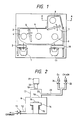
- Fig. 1 shows a continuously treating apparatus which is capable of continuously carrying out the etching treatment and the post-etch treatment under vacuum condition.
- a buffer chamber 3 defines space from load lock chambers 4, 9 through an etching chamber 6 up to a post-etch treatment chamber 8.
- each of the buffer chamber 3, load lock chambers 4, 9, etching chamber 6, and post-etch treatment chamber 8 can be independently partitioned by air-tight means and can be evacuated by an exhaust device (not shown).
- a load-side cassette 1 is disposed to be opposed to the load lock chamber 4, and a go-straight arm 2 is arranged therebetween.
- An unload-side cassette 11 is disposed to be opposed to the load lock chamber 9, and a go-straight arm 10 is arranged therebetween.
- a sample (wafer in this case) that is to be treated is introduced into the load lock chamber 4 which is open to the atmosphere from the load-side cassette 1 by the go-straight arm 2. Thereafter, the load lock chamber 4 is air-tightly closed and is evacuated by the vacuum device from the condition of atmospheric pressure to a vacuum condition. Then, the load lock chamber 4, the buffer chamber 3, and the etching chamber 6 are communicated with each other, and the sample is carried by a swing arm 5 into the etching chamber 6 evacuated into a vacuum condition via the buffer chamber 3 that is also evacuated into a vacuum condition. Thereafter, the etching chamber 6 is air-tightly closed to carry out a predetermined etching treatment therein.
- the etching chamber 6, buffer chamber 3 and post-etch treatment chamber 8 are communicated with each other, and the sample is carried by a swing arm 7 into the post-etch treatment chamber 8 that is evacuated into a vacuum condition via the buffer chamber 3 that is evacuated into a vacuum condition. Thereafter, the post-etch treatment chamber 8 is air-tightly sealed to carry out a predetermined post-etch treatment therein.
- the post-etch treatment chamber 8, the buffer chamber 3 and the load lock chamber 9 are communicated with each other, and the sample is carried by the swing arm 7 into the load lock chamber 9 that is evacuated into a vacuum condition via the buffer chamber 3 that has been evacuated to the vacuum condition.
- the load lock chamber 9 is air-tightly closed, and a leakage gas such as N2 gas is introduced into the load lock chamber 9 to elevate the pressure up to the atmospheric pressure. Then, the load lock chamber 9 is opened, and the treated sample is delivered from the load lock chamber 9 by the go-straight arm 10 and is stored in the unload-side cassette 11 to complete a series of treatments.
- a leakage gas such as N2 gas
- Fig. 2 is a vertical section view of the sample treatment apparatus illustrating the portion of the post-etch treatment chamber 8 of Fig. 1.
- a plasma generating chamber 17 that is partitioned by an aluminum porous plate 18.
- the upper opening of the plasma generating chamber 17 is closed by a window 19 of quartz, and a microwave waveguide 20 having a microwave oscillator 21 at the end is mounted on the opening.
- the plasma generating chamber 17 is provided with a gas feed port 22 to which is connected a gas feed pipe 23 to feed a treatment gas into the plasma generating chamber 17 from a gas feed source (not shown) via flow rate control valves 24 and 25.
- the post-etch treatment chamber 8 is provided with an exhaust port 12 to which is connected a vacuum device (not shown) via a pressure control valve 13 to evacuate the interior of the post-etch treatment chamber 8.
- the post-etch treatment chamber 8 is further provided with a sample plate 14 on which a sample 16 is placed being opposed to the plasma generating chamber 17.
- the sample plate 14 is equipped with a heating device 15 for heating the sample 16.
- the microwaves of a frequency of, in this case, 2.45 GHz generated by the microwave oscillator 21 are guided into the plasma generating chamber 17 propagating through the microwave waveguide 20 and the window 19.
- the microwaves introduced into the plasma generating chamber 17 excite the treatment gas that is introduced into the plasma generating chamber 17.
- a plasma is generated in the plasma generating chamber 17.
- the aluminum porous plate 18 provided between the plasma generating chamber 17 and the post-etch treatment chamber 8 reflects the microwaves so as not to enter into the post-etch treatment chamber 8, and prevents the generation of plasma in the post-etch treatment chamber 8.
- the plasma and chiefly radical components in the plasma generating chamber 17 that has passed through the porous plate 18 is guided onto the sample 16 carried by the exhaust stream of the post-etch treatment chamber 8.
- the sample 16 on which the wiring film (aluminum-containing wiring material) is formed is etched using a halogen-type gas.
- the etching treatment is carried out by using an RIE apparatus or a microwave apparatus. Described below is a case of the etching treatment carried out using, for example, a microwave etching apparatus in the presence of magnetic field wherein the sample to be treated is placed on the sample plate, a plasma of the treatment gas is formed by the action of electric field of the microwaves and magnetic field of the solenoid coil, and the sample is etched by the application of a high-frequency bias.
- the sample 16 on which the wiring film is formed is obtained by forming a heat oxidized film (SiO2) maintaining a thickness of 600nm on the silicon substrate, and then forming a TiN film, an Al-Si (1%) - Cu (0.5%) film, and TiN film thereon maintaining thicknesses of 100nm, 700nm and 50nm, respectively, and then forming a resist film thereon maintaining a thickness of 1800nm.
- the wiring pattern is formed in the resist film which is used as a mask for etching.
- a mixture gas consisting of BCl3 (60cc/min.) and Cl2 (90cc/min.) is used as the halogen-type gas.
- the etching treatment is carried out under the conditions of a pressure of 2.1 Pa, microwave current of 300mA, and high-frequency electric power of 90 watts.
- the resist which is a masking material remains on the wiring pattern that is formed by etching
- halogen which, in this case, is chlorine component remains in the resist and on the surface of the resist.
- the residual adhered matter consisting of aluminum, chlorine, carbon, hydrogen, etc. remains on the side walls of the wiring pattern.
- the sample 16 on which the resist and residual adhered matter remain is sent to the post-etch treatment chamber 8 to effect the post-etch treatment which is carried out as described below. That is, the flow rates of an oxygen gas (O2) and a methanol gas (CH3OH) containing hydrogen component are adjusted by the flow rate control valves 24 and 25, and these gases are mixed together and are introduced into the plasma generating chamber 17.
- the flow rate of oxygen gas is 400cc/min.
- the flow rate of methanol gas is 80cc/min.
- the pressure in the post-etch treatment chamber 8 is 160 Pa.
- the microwaves are introduced into the plasma generating chamber 17 from the microwave oscillator 21. For instance, the microwave output in this case is 400mA.
- a plasma of hydrogen component (H), oxygen component (O) and other components is generated in the plasma generating chamber 17.
- the plasma consisting chiefly of radicals is guided into the post-etch treatment chamber 8 accompanying the evacuating exhaust stream.
- Radicals are chiefly comprised of hydrogen and oxygen.
- the hydrogen radicals react with the chlorine component (Cl) in the residual adhered matter (Al, Cl, C, H, etc.) to form hydrogen chloride (HCl) which volatilizes or forms H2O to dissolve the elute chlorine component contributing presumably to removing residual chlorine component that is a cause of corrosion to the wiring film.
- the oxygen radicals react with the resist to form CO and CO2 that volatilize, so that the organic components composed chiefly of resist are removed.
- the wiring film after the etching treatment is treated using the plasma of the treatment gas consisting of a mixture of methanol gas and oxygen gas, and whereby the resist and the residual adhered matter remaining on the sample are removed and, further, the chlorine components remaining on the surface and inside the sample which cause corrosion are removed.
- the treatment gas consisting of a mixture of methanol gas and oxygen gas
- the ashing treatment can be effected at the same time.
- the sample plate 14 is heated by the heating device 15 to heat the sample that is being treated with plasma. Therefore, the chemical reaction of the residual adhered matter or the resist with the radicals is assisted to more efficiently remove the residual matter (residual adhered matter and resist) after the etching treatment.
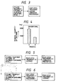
- Fig. 4 is a diagram showing the residual chlorine quantity reducing effect according to this embodiment.
- the treatment A of Fig. 3 shows the residual chlorine quantity of the case when the treatment is effected for two minutes in a customary manner using the plasma of a mixture gas consisting of oxygen (O2) and carbon tetrafluoride (CF4).
- the treatment B shows the residual chlorine quantity of the case when the treatment is effected for one minute using a mixture gas consisting of methanol (CH3OH) and oxygen (O2).
- the additional treatment is effected for one minute using the plasma of oxygen to prevent the resist from remaining after the treatment using the mixture gas.
- the sample is an aluminum-film wafer with a 6-inch wiring pattern, the aluminum film having a thickness of 800nm.
- the treatment A is carried out under the conditions of an oxygen flow rate of 400cc/min, a carbon tetrafluoride flow rate of 20cc/min and a treatment pressure of 160 Pa.
- the treatment B is first carried out under the conditions of a methanol flow rate of 80cc.min, an oxygen flow rate of 400cc/min and a treatment pressure of 160 Pa., and is then carried out under the conditions of an oxygen flow rate of 400cc/min and a treatment pressure of 160 Pa.
- the treatment B is carried out while setting the sample plate temperature at 250°C such that the resist ashing rate becomes nearly equal to the values of when a mixture gas of oxygen and carbon tetrafluoride is used.
- the sample plate 14 should be set at a temperature of 200°C to 350°C from the relationship of the ashing rate of the resist and the thermal damage to the aluminum film.
- the treatment with the plasma of a gas containing hydrogen and oxygen according to this embodiment makes it possible to decrease the residual chlorine content to less than about one-half compared with that of the prior art. Therefore, the corrosion prevention performance of longer than 24 hours to obtained even under clean room environment.
- the chlorine-containing gas was used as the halogen-type gas for the etching treatment of the wiring film, the same effects are also obtained even when the bromine-type gas is used.
- the methanol gas and the oxygen gas are mixed together to produce a plasma, in order to carry out the corrosion prevention treatment and the ashing treatment simultaneously.
- the resist component (C, H, etc.) is removed (ashing treatment) with the plasma of oxygen gas (O2) after the etching treatment. Then, the treatment gas is changed, and the residual matter (resist component, etc.) and the chlorine component are removed (corrosion prevention treatment) with the plasma of, in this case, the treatment gas of a mixture of oxygen gas (O2) and methanol gas (CH3OH).
- the treatment gas used for the corrosion prevention treatment may be a treatment gas consisting of a mixture of an inert gas such as helium or argon, a gas having N2O or O3 and H components (such as methanol (CH3OH), ethanol (C2H5OH), acetone (CH3COCH3), hydrogen (H2), ethane (CH4) or the like), or a gas containing hydrogen component only, in addition to the treatment gas consisting of a mixture of oxygen gas (O2) and methanol gas (CH3OH).
- an inert gas such as helium or argon
- a gas having N2O or O3 and H components such as methanol (CH3OH), ethanol (C2H5OH), acetone (CH3COCH3), hydrogen (H2), ethane (CH4) or the like
- a gas containing hydrogen component only in addition to the treatment gas consisting of a mixture of oxygen gas (O2) and methanol gas (CH3OH).
- the residual adhered matter and chlorine component adhered to the resist are removed with the plasma of a treatment gas of a mixture of an inert gas without containing oxygen component and a gas containing hydrogen component after the etching treatment and, then, the treatment gas is changed in order to remove the resist with the plasma of the oxygen gas (O2).
- the above-mentioned gases can be used as the treatment gases.
- the treatment may be carried out while switching these gases.
- the chlorine quantity remaining in the wiring film after the etching treatment can be greatly reduced compared with that of the prior art, and high corrosion prevention performance is imparted to the wiring film after the etching treatment.
- the apparatus in the post-etch treatment portion in this embodiment is constituted by providing the porous plate 18 between the plasma generating chamber 17 and the post-etch treatment chamber 8 as shown in Fig. 2. It is, however, also allowable to directly treat the sample 16 with the plasma generated in the plasma generating chamber 17 without employing the porous plate. Further, the plasma is generated using microwaves. It is, however, also allowable to employ an RIE apparatus of the type of parallel flat plates using high-frequency electric power or any other system using high-frequency electric power such as a cylindrical-type apparatus, provided it is capable of generating plasma that contains hydrogen component and oxygen component.
- the etching treatment and the post-etch treatment are incorporated in the same apparatus as shown in Fig. 1 and are continuously carried out.
- the invention is in no way limited thereto only. That is, when the resist and the residual adhered matter are to be removed simultaneously, the subsequent additional treatment with the plasma of oxygen may be carried out in a separate treatment chamber which is provided on the outside of the apparatus that is shown in Fig. 1.
- the resist may be removed by the widely known ashing treatment using the plasma of a mixture gas consisting of oxygen gas and a fluorine-type gas.
- the ashing treatment with the plasma of a mixture gas of oxygen gas and fluorine- type gas is effective for the corrosion prevention treatment particularly when a silicon-type material is contained in the resist material for forming pattern.
- the silicon-type material silicon-type inorganic resist or silicon photoresist
- the ashing treatment with the oxygen radicals permit the silicon in the resist material to react with oxygen radicals to form silicon oxide that stays thereon, making it difficult to sufficiently carry out the ashing treatment for the resist.
- the remaining resist causes the wiring to corrode due to the residual chlorine or stays as foreign matter when an insulating film is to be formed on the wiring film causing poor insulation of the circuit, and deteriorates the yields of production. Therefore, the resist should be removed as much as possible.
- the ashing treatment with the plasma of mixture gas of oxygen gas and fluorine-type gas is carried out after the plasma treatment (corrosion prevention treatment) that uses methanol or the mixture gas of methanol and oxygen, and that is effected after the etching treatment. Therefore, when the silicon-type material is used as the resist material component, the residual adhered matter and the resist that stay on the wiring film after the etching treatment can be effectively removed to accomplish high corrosion prevention performance.
- the sample plate should be maintained at a temperature of lower than 50°C when the sample 17 is composed of a barrier metal in order to prevent side etching of TiN film or TiW film that lies under the wiring film.
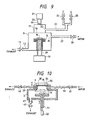
- the post-etch treatment chamber 8 is provided with a feed port 26 to which is connected a feed pipe 27 that is connected, via a flow rate control valve 28, to a gas feed source (not shown) for adsorption/desorption treatment, so that a gas for adsorption/desorption treatment can be supplied into the post-etch treatment chamber 8.
- the sample 16 after the etching treatment with the plasma of a halogen-type gas is subjected to the treatment for removing resist in the post-etch treatment chamber 8 using the plasma of an oxygen gas which is one of the methods mentioned in the foregoing first embodiment. Thereafter, the residual components that cause corrosion are removed as described below.
- the gas for adsorption/desorption treatment is supplied at a controlled flow rate into the post-etch treatment chamber 8 from the source (not shown) of feeding the gas for adsorption/desorption treatment via the flow rate control valve 28 and the feed pipe 27.
- the gas in this case, is that of pure water component or, concretely, vaporized gas of pure water.
- the pressure control valve 13 for controlling the pressure in the post-etch treatment chamber 8 is maintained closed. This causes the pressure in the post-etch treatment chamber 8 to rise.
- a preset pressure in the post-etch treatment chamber is exceeded, i.e., when a pressure region denoted by A in Fig.
- the sample plate temperature in this case is about 20°C, and the operation is repeated twice in which the pressure in the post-etch treatment chamber 8 is raised from 67 Pa to 4000 Pa and is decreased again down to 67 Pa each time.
- the component that causes corrosion or halogen component in this case, is dissolved and diluted on the sample surface after the ashing treatment owing to the adsorption of the introduced vaporized gas of pure water and the dropping of liquid formed by the rise in gas pressure.
- the interior in the post-etch treatment chamber 8 is evacuated (the pressure in the post-etch treatment chamber 8 is decreased into a region denoted by B in Fig. 8) to promote the vaporization and desorption of pure water in which are dissolved halogen components adhered onto the sample surface.
- This makes it possible to greatly decrease the amount of halogen components adhered on the sample, and the corrosion protection performance of longer than 24 hours is obtained even under a clean room environment.
- the second embodiment which greatly decreases the amount of halogen remaining after the etching treatment and ashing treatment of the wiring film, it is allowed to obtain improved corrosion prevention performance. Moreover, no water-washing apparatus is needed. In addition, resist removing means is incorporated. Therefore, the treatment is carried out consistently in series from the etching treatment through the resist removal treatment up to the corrosion prevention treatment, making it possible to shorten the time for carrying samples among the treatment apparatuses and to shorten the waiting time, contributing to improving production efficiency. Moreover, since no water-washing apparatus is needed, the apparatus can be realized in a compact size.
- the apparatus used in this embodiment consists of the apparatus shown in Fig. 2 but which is further equipped with temperature adjusting means (consisting of a constant temperature water vessel 30 and a cooling water flow path 29) for controlling the temperature of the sample plate 14.
- the sample 16 is subjected to the etching treatment and the resist removal treatment, and the vaporized gas of pure water is introduced into the post-etch treatment chamber 8 in order to effect the adsorption and desorption of components that remain and cause corrosion to the sample 16.
- the sample plate 14 on which the sample 16 is placed is maintained at a temperature of 0°C to 20°C which is lower than room temperature owing to the temperature adjusting means.
- the sample plate 14 and the sample 16 have a temperature lower than the periphery thereof, e.g., lower than the side walls of the post-etch treatment chamber 8 at the time of adsorption and desorption of the introduced gas, and the introduced gas is adsorbed in a concentrated manner. Therefore, the components, i.e., halogen components that are remaining on the sample 16 and that are causes of corrosion, are dissolved and diluted efficiently, enabling the halogen quantity remaining after the desorption to be greatly decreased.
- This embodiment makes it possible to further enhance the corrosion prevention performance than the aforementioned embodiments.
- the resist is removed after the etching treatment and, then, the adsorption and desorption are carried out to decrease the halogen component that remains on the sample to corrode it.
- the desorption promotion treatment in this embodiment, the sample is heated while treating it with the plasma of oxygen after the adsorption and desorption
- This makes it possible to vaporize and remove the water content containing halogen component remaining after the adsorption and desorption and, hence, to obtain higher corrosion preventing performance than that of the second embodiment.
- the load lock chamber 9 shown in Fig. 1 is equipped with heating means to heat the sample 16 that is to be treated, and feeding means is provided to feed a gas for adsorption/desorption treatment into the load lock chamber 9.
- the heating means consists of a heating device 34 placed on a quartz glass 33 that hermetically closes the upper opening of the load lock chamber 9.
- the heating device 34 in this case is a lamp heater.
- the feeding means for feeding a gas for adsorption/desorption treatment consists as in the second embodiment of providing the load lock chamber 9 with a feed port 35 to which is connected, via a flow rate control valve 37, a feed pipe 36 that is connected to the source (not shown) that feeds the gas for adsorption/desorption treatment.
- Reference numeral 38 denotes an exhaust port formed in the load lock chamer 9.
- An exhaust device (not shown) is connected to the exhaust port 38 via an exhaust pipe 39 and a pressure control valve 40.
- Reference numeral 41 denotes an exhaust port formed in the buffer chamber 3.
- An exhaust device (not shown) is connected to the exhaust port 41 via a pressure control valve 42.
- the sample plate 31 moves up and down, and comes in contact with the upper opening in the buffer chamber 3 to form the load lock chamber 9.
- the device for pushing up the sample 16 works to easily hand the sample 16 over to the carrier device such as the swing arm at the time of delivering the sample into or out of the buffer chamber 3 or the load lock chamber 9.
- the load lock chamber 9 is the one which communicates the vacuum chamber with the open atmosphere. In order to evacuate into vacuum condition or to return the pressure to the atmospheric pressure, the load lock chamber 9 has space which is as small as possible such that the pressure condition can be quickly changed.
- the etching treatment and the resist removal treatment are carried out in the same manner as in the afore-mentioned first embodiment. That is, the etching treatment is effected with the plasma of the halogen-type gas in the etching chamber and, then, the resist is removed in the post-etch treatment chamber using the plasma of, for example, an oxygen gas which is one of the methods mentioned in the foregoing first embodiment.
- the sample 16 is introduced into the load lock chamber 9 shown in Fig. 10, and the halogen components that are causes of corrosion are removed as described below.
- the gas for adsorption/desorption treatment such as vaporized gas of pure water is supplied at a controlled flow rate into the load lock chamber 9 from the source (not shown) of feeding gas for adsorption/desorption treatment via the flow rate control valve 37 and the feed pipe 36.
- the pressure control valve 40 for controlling the pressure in the load lock chamber 9 is maintained closed. This causes the pressure in the load lock chamber 9 to rise.
- the operation is repeated twice in which the sample plate temperature is maintained at about 20°C, the pressure in the post-etch treatment chamber 8 is raised from 67 Pa to 4000 Pa and is decreased again to 67 Pa each time, in the same manner as in the processing of the aforementioned second embodiment.
- the sample 16 is heated by the heating device 34 (lamp heater).
- the halogen components that are causes of corrosion are dissolved and eluted on the surface of the sample after the resist removal treatment owing to the adsorption of the introduced gas and the liquefaction by the rise in the gas pressure. Thereafter, the interior of the load lock chamber 9 is evacuated to promote the vaporization and desorption of pure water in which are dissolved and diluted halogen components remaining on the sample surface. This makes it possible to greatly decrease the amount of halogen components adhered to and remaining on the sample.
- the heating device 34 furthermore, the water content remaining after the adsorption/desorption operation is removed by evaporation. Therefore, the effect by the halogen component-containing water decreases, and high corrosion protection performance is obtained.
- This embodiment makes it possible to obtain high corrosion prevention performance as described above. Furthermore, since the load lock chamber 9 having small inner space is used as the treatment chamber, the vaporized gas of pure water needs be supplied in small amounts compared with the desorption treatment of residual halogen components by dissolution and delution in the post-etch treatment chamber 8. Furthermore, a good response in the pressure change enables the throughput to be improved. Further, since the sample 16 is directly heated by the heating device 34, the time of desorption treatment can be shortened compared with the time of desorption treatment by the heating with oxygen plasma in the post-etch treatment chamber 8 mentioned in the foregoing third embodiment. This makes it possible to increase the amount of treating the samples per a unit time in carrying out the treatment continuously and consistently.
- the halogen components are dissolved and diluted using the vaporized gas of pure water in the load lock chamber 9, and the pure water in which the halogen components are dissolved and diluted is subjected to the vaporization/desorption treatment, and the water remaining after the adsorption/desorption operation by the heating device 34 is removed by vaporization. It is, however, also allowable to dissolve and dilute the halogen components using the vaporized gas of pure water in the post-etch treatment chamber 8 followed by the evaporation/desorption treatment of pure water in which the halogen components are dissolved and diluted, and to remove by vaporization the water that remains after the adsorption/desorption operation using the heating device 34 in the load lock chamber 9. In this case, the load lock chamber 9 should be provided with the heating device 34 only.
- the components that are causes of corrosion after the etching treatment of the wiring film are effectively decreased, and high corrosion prevention performance is imparted to the wiring film.
- the apparatus is constituted in a compact size contributing to improving the productivity.
Landscapes
- Engineering & Computer Science (AREA)
- Chemical & Material Sciences (AREA)
- Power Engineering (AREA)
- Manufacturing & Machinery (AREA)
- Microelectronics & Electronic Packaging (AREA)
- Computer Hardware Design (AREA)
- Physics & Mathematics (AREA)
- Condensed Matter Physics & Semiconductors (AREA)
- General Physics & Mathematics (AREA)
- Mechanical Engineering (AREA)
- Organic Chemistry (AREA)
- Metallurgy (AREA)
- Materials Engineering (AREA)
- Drying Of Semiconductors (AREA)
- ing And Chemical Polishing (AREA)
- Internal Circuitry In Semiconductor Integrated Circuit Devices (AREA)
Priority Applications (1)
| Application Number | Priority Date | Filing Date | Title |
|---|---|---|---|
| EP19970107985 EP0809283A3 (fr) | 1989-08-28 | 1990-08-20 | Procédé de traitement de substrat |
Applications Claiming Priority (9)
| Application Number | Priority Date | Filing Date | Title |
|---|---|---|---|
| JP218523/89 | 1989-08-28 | ||
| JP1218523A JPH0793293B2 (ja) | 1989-08-28 | 1989-08-28 | 後処理方法 |
| JP21852389 | 1989-08-28 | ||
| JP284711/89 | 1989-11-02 | ||
| JP28471189 | 1989-11-02 | ||
| JP1284711A JP2585442B2 (ja) | 1989-11-02 | 1989-11-02 | 被処理物の連続処理方法 |
| JP117596/90 | 1990-05-09 | ||
| JP11759690 | 1990-05-09 | ||
| JP11759690A JPH0415919A (ja) | 1990-05-09 | 1990-05-09 | 後処理方法 |
Related Child Applications (1)
| Application Number | Title | Priority Date | Filing Date |
|---|---|---|---|
| EP19970107985 Division EP0809283A3 (fr) | 1989-08-28 | 1990-08-20 | Procédé de traitement de substrat |
Publications (2)
| Publication Number | Publication Date |
|---|---|
| EP0416774A1 true EP0416774A1 (fr) | 1991-03-13 |
| EP0416774B1 EP0416774B1 (fr) | 2000-11-15 |
Family
ID=27313413
Family Applications (2)
| Application Number | Title | Priority Date | Filing Date |
|---|---|---|---|
| EP19900309106 Expired - Lifetime EP0416774B1 (fr) | 1989-08-28 | 1990-08-20 | Procédé de traitement d'un échantillon de matériau contenant de l'aluminium |
| EP19970107985 Withdrawn EP0809283A3 (fr) | 1989-08-28 | 1990-08-20 | Procédé de traitement de substrat |
Family Applications After (1)
| Application Number | Title | Priority Date | Filing Date |
|---|---|---|---|
| EP19970107985 Withdrawn EP0809283A3 (fr) | 1989-08-28 | 1990-08-20 | Procédé de traitement de substrat |
Country Status (4)
| Country | Link |
|---|---|
| US (4) | US5380397A (fr) |
| EP (2) | EP0416774B1 (fr) |
| KR (1) | KR0155380B1 (fr) |
| DE (1) | DE69033663T2 (fr) |
Cited By (11)
| Publication number | Priority date | Publication date | Assignee | Title |
|---|---|---|---|---|
| EP0489179A1 (fr) * | 1990-06-27 | 1992-06-10 | Fujitsu Limited | Procede de fabrication d'un circuit integre a semi-conducteurs et appareil de fabrication correspondant |
| WO1995021458A1 (fr) * | 1994-02-03 | 1995-08-10 | Applied Materials, Inc. | Decapage, passivation et inhibition de la corrosion de substrats a semi-conducteurs |
| US5545289A (en) * | 1994-02-03 | 1996-08-13 | Applied Materials, Inc. | Passivating, stripping and corrosion inhibition of semiconductor substrates |
| EP0740333A2 (fr) * | 1995-04-21 | 1996-10-30 | Nec Corporation | Méthode de brûlage de photoréserve à haute vitesse |
| US5578163A (en) * | 1991-10-21 | 1996-11-26 | Seiko Epson Corporation | Method of making an aluminum containing interconnect without hardening of a sidewall protection layer |
| US5599743A (en) * | 1994-04-07 | 1997-02-04 | Matsushita Electronics Corporation | Method of manufacturing a semiconductor device |
| US6440864B1 (en) | 2000-06-30 | 2002-08-27 | Applied Materials Inc. | Substrate cleaning process |
| US6692903B2 (en) | 2000-12-13 | 2004-02-17 | Applied Materials, Inc | Substrate cleaning apparatus and method |
| EP1500720A1 (fr) * | 2003-07-24 | 2005-01-26 | Anelva Corporation | Procédé de gravure sèche de matériaux magnétiques |
| EP1916703A2 (fr) * | 2006-10-26 | 2008-04-30 | Applied Materials, Inc. | Procédé intégré d'élimination de résidus halogènes de substrats attaqués par un procédé thermique |
| US10535776B2 (en) | 2011-10-19 | 2020-01-14 | Semiconductor Energy Laboratory Co., Ltd. | Semiconductor device and manufacturing method thereof |
Families Citing this family (50)
| Publication number | Priority date | Publication date | Assignee | Title |
|---|---|---|---|---|
| EP0416774B1 (fr) * | 1989-08-28 | 2000-11-15 | Hitachi, Ltd. | Procédé de traitement d'un échantillon de matériau contenant de l'aluminium |
| JP2644912B2 (ja) | 1990-08-29 | 1997-08-25 | 株式会社日立製作所 | 真空処理装置及びその運転方法 |
| US7089680B1 (en) | 1990-08-29 | 2006-08-15 | Hitachi, Ltd. | Vacuum processing apparatus and operating method therefor |
| USRE39824E1 (en) * | 1990-08-29 | 2007-09-11 | Hitachi, Ltd. | Vacuum processing apparatus and operating method with wafers, substrates and/or semiconductors |
| USRE39756E1 (en) * | 1990-08-29 | 2007-08-07 | Hitachi, Ltd. | Vacuum processing operating method with wafers, substrates and/or semiconductors |
| JP2674488B2 (ja) * | 1993-12-01 | 1997-11-12 | 日本電気株式会社 | ドライエッチング室のクリーニング方法 |
| US5744049A (en) * | 1994-07-18 | 1998-04-28 | Applied Materials, Inc. | Plasma reactor with enhanced plasma uniformity by gas addition, and method of using same |
| US6060397A (en) * | 1995-07-14 | 2000-05-09 | Applied Materials, Inc. | Gas chemistry for improved in-situ cleaning of residue for a CVD apparatus |
| US5785875A (en) * | 1996-02-13 | 1998-07-28 | Micron Technology, Inc. | Photoresist removal process using heated solvent vapor |
| US5700740A (en) * | 1996-03-25 | 1997-12-23 | Taiwan Semiconductor Manufacturing Company Ltd | Prevention of corrosion of aluminum interconnects by removing corrosion-inducing species |
| US6170428B1 (en) * | 1996-07-15 | 2001-01-09 | Applied Materials, Inc. | Symmetric tunable inductively coupled HDP-CVD reactor |
| US5776832A (en) * | 1996-07-17 | 1998-07-07 | Taiwan Semiconductor Manufacturing Company Ltd. | Anti-corrosion etch process for etching metal interconnections extending over and within contact openings |
| US6310300B1 (en) | 1996-11-08 | 2001-10-30 | International Business Machines Corporation | Fluorine-free barrier layer between conductor and insulator for degradation prevention |
| US6303045B1 (en) * | 1997-03-20 | 2001-10-16 | Lam Research Corporation | Methods and apparatus for etching a nitride layer in a variable-gap plasma processing chamber |
| US6168672B1 (en) * | 1998-03-06 | 2001-01-02 | Applied Materials Inc. | Method and apparatus for automatically performing cleaning processes in a semiconductor wafer processing system |
| WO1999046810A1 (fr) * | 1998-03-12 | 1999-09-16 | Hitachi, Ltd. | Procede permettant de traiter la surface d'un echantillon |
| US6455232B1 (en) * | 1998-04-14 | 2002-09-24 | Applied Materials, Inc. | Method of reducing stop layer loss in a photoresist stripping process using a fluorine scavenger |
| US6254717B1 (en) * | 1998-04-23 | 2001-07-03 | Sandia Corporation | Method and apparatus for monitoring plasma processing operations |
| US6221752B1 (en) * | 1998-08-20 | 2001-04-24 | United Microelectronics Corp. | Method of mending erosion of bonding pad |
| US6410417B1 (en) * | 1998-11-05 | 2002-06-25 | Promos Technologies, Inc. | Method of forming tungsten interconnect and vias without tungsten loss during wet stripping of photoresist polymer |
| US6368517B1 (en) * | 1999-02-17 | 2002-04-09 | Applied Materials, Inc. | Method for preventing corrosion of a dielectric material |
| US6627588B1 (en) | 1999-03-11 | 2003-09-30 | Georgia Tech Research Corporation | Method of stripping photoresist using alcohols |
| US6238582B1 (en) | 1999-03-30 | 2001-05-29 | Veeco Instruments, Inc. | Reactive ion beam etching method and a thin film head fabricated using the method |
| US20030015496A1 (en) * | 1999-07-22 | 2003-01-23 | Sujit Sharan | Plasma etching process |
| US6559076B1 (en) | 1999-08-19 | 2003-05-06 | Micron Technology, Inc. | Method of removing free halogen from a halogenated polymer insulating layer of a semiconductor device |
| US6228563B1 (en) * | 1999-09-17 | 2001-05-08 | Gasonics International Corporation | Method and apparatus for removing post-etch residues and other adherent matrices |
| JP2001110663A (ja) * | 1999-10-08 | 2001-04-20 | Hitachi Ltd | 試料の処理方法および処理装置並びに磁気ヘッドの製作方法 |
| US6682659B1 (en) | 1999-11-08 | 2004-01-27 | Taiwan Semiconductor Manufacturing Company | Method for forming corrosion inhibited conductor layer |
| US20020076917A1 (en) * | 1999-12-20 | 2002-06-20 | Edward P Barth | Dual damascene interconnect structure using low stress flourosilicate insulator with copper conductors |
| US6852636B1 (en) * | 1999-12-27 | 2005-02-08 | Lam Research Corporation | Insitu post etch process to remove remaining photoresist and residual sidewall passivation |
| KR100373853B1 (ko) * | 2000-08-11 | 2003-02-26 | 삼성전자주식회사 | 반도체소자의 선택적 에피택시얼 성장 방법 |
| US6564811B2 (en) * | 2001-03-26 | 2003-05-20 | Intel Corporation | Method of reducing residue deposition onto ash chamber base surfaces |
| US7204669B2 (en) * | 2002-07-17 | 2007-04-17 | Applied Materials, Inc. | Semiconductor substrate damage protection system |
| WO2004027826A2 (fr) * | 2002-09-18 | 2004-04-01 | Mattson Technology, Inc. | Systeme et procede de retrait d'une matiere |
| US6920891B2 (en) * | 2002-10-05 | 2005-07-26 | Taiwan Semiconductor Manufacturing Co., Ltd. | Exhaust adaptor and method for chamber de-gassing |
| TWI232991B (en) * | 2002-11-15 | 2005-05-21 | Nec Lcd Technologies Ltd | Method for manufacturing an LCD device |
| US7232766B2 (en) * | 2003-03-14 | 2007-06-19 | Lam Research Corporation | System and method for surface reduction, passivation, corrosion prevention and activation of copper surface |
| US7009281B2 (en) * | 2003-03-14 | 2006-03-07 | Lam Corporation | Small volume process chamber with hot inner surfaces |
| US7078344B2 (en) * | 2003-03-14 | 2006-07-18 | Lam Research Corporation | Stress free etch processing in combination with a dynamic liquid meniscus |
| US7217649B2 (en) * | 2003-03-14 | 2007-05-15 | Lam Research Corporation | System and method for stress free conductor removal |
| TWI281473B (en) * | 2003-12-19 | 2007-05-21 | Ind Tech Res Inst | Biomarkers for liver diseases and method for using same |
| US20060063388A1 (en) * | 2004-09-23 | 2006-03-23 | Taiwan Semiconductor Manufacturing Company, Ltd. | Method for using a water vapor treatment to reduce surface charge after metal etching |
| KR100688778B1 (ko) * | 2004-12-27 | 2007-03-02 | 동부일렉트로닉스 주식회사 | 반도체 소자의 제조 방법 |
| KR100688777B1 (ko) * | 2004-12-27 | 2007-03-02 | 동부일렉트로닉스 주식회사 | 반도체 소자의 제조 방법 |
| KR100608435B1 (ko) * | 2004-12-30 | 2006-08-02 | 동부일렉트로닉스 주식회사 | 반도체 소자의 애싱 방법 |
| US7655571B2 (en) * | 2006-10-26 | 2010-02-02 | Applied Materials, Inc. | Integrated method and apparatus for efficient removal of halogen residues from etched substrates |
| US7678715B2 (en) * | 2007-12-21 | 2010-03-16 | Applied Materials, Inc. | Low wet etch rate silicon nitride film |
| US20110079242A1 (en) * | 2009-10-07 | 2011-04-07 | Werner Reiss | Plasma cleaning of wire strands |
| US9018108B2 (en) | 2013-01-25 | 2015-04-28 | Applied Materials, Inc. | Low shrinkage dielectric films |
| JP6349796B2 (ja) * | 2014-03-11 | 2018-07-04 | 東京エレクトロン株式会社 | プラズマ処理装置、薄膜トランジスターの製造方法及び記憶媒体 |
Citations (3)
| Publication number | Priority date | Publication date | Assignee | Title |
|---|---|---|---|---|
| EP0078224A1 (fr) * | 1981-10-28 | 1983-05-04 | FAIRCHILD CAMERA & INSTRUMENT CORPORATION | Inhiber la corrosion de métallisation d'aluminium |
| EP0140201A2 (fr) * | 1983-10-04 | 1985-05-08 | Asahi Glass Company Ltd. | Procédé d'attaque sèche |
| EP0247603A2 (fr) * | 1986-05-29 | 1987-12-02 | Fujitsu Limited | Méthode pour enlever une résine photosensible sur un alliage d'aluminium |
Family Cites Families (13)
| Publication number | Priority date | Publication date | Assignee | Title |
|---|---|---|---|---|
| US4138306A (en) * | 1976-08-31 | 1979-02-06 | Tokyo Shibaura Electric Co., Ltd. | Apparatus for the treatment of semiconductors |
| JPS5841766B2 (ja) * | 1978-12-28 | 1983-09-14 | 富士通株式会社 | 半導体装置の製造方法 |
| US4325984B2 (en) * | 1980-07-28 | 1998-03-03 | Fairchild Camera & Inst | Plasma passivation technique for the prevention of post-etch corrosion of plasma-etched aluminum films |
| KR910003169B1 (ko) * | 1985-11-12 | 1991-05-20 | 가부시끼가이샤 한도다이 에네르기 겐뀨소 | 반도체 장치 제조 방법 및 장치 |
| JPS6362233A (ja) * | 1986-09-03 | 1988-03-18 | Mitsubishi Electric Corp | 反応性イオンエツチング装置 |
| EP0305946B1 (fr) * | 1987-08-28 | 1996-10-30 | Kabushiki Kaisha Toshiba | Procédé d'enlèvement de films organique et/ou minéraux par plasma |
| US4961820A (en) * | 1988-06-09 | 1990-10-09 | Fujitsu Limited | Ashing method for removing an organic film on a substance of a semiconductor device under fabrication |
| JP2890432B2 (ja) * | 1989-01-10 | 1999-05-17 | 富士通株式会社 | 有機物の灰化方法 |
| JP2528962B2 (ja) * | 1989-02-27 | 1996-08-28 | 株式会社日立製作所 | 試料処理方法及び装置 |
| US4985113A (en) * | 1989-03-10 | 1991-01-15 | Hitachi, Ltd. | Sample treating method and apparatus |
| EP0416774B1 (fr) * | 1989-08-28 | 2000-11-15 | Hitachi, Ltd. | Procédé de traitement d'un échantillon de matériau contenant de l'aluminium |
| US5221424A (en) * | 1991-11-21 | 1993-06-22 | Applied Materials, Inc. | Method for removal of photoresist over metal which also removes or inactivates corosion-forming materials remaining from previous metal etch |
| US5545289A (en) * | 1994-02-03 | 1996-08-13 | Applied Materials, Inc. | Passivating, stripping and corrosion inhibition of semiconductor substrates |
-
1990
- 1990-08-20 EP EP19900309106 patent/EP0416774B1/fr not_active Expired - Lifetime
- 1990-08-20 DE DE1990633663 patent/DE69033663T2/de not_active Expired - Fee Related
- 1990-08-20 EP EP19970107985 patent/EP0809283A3/fr not_active Withdrawn
- 1990-08-27 KR KR1019900013207A patent/KR0155380B1/ko not_active IP Right Cessation
-
1992
- 1992-10-27 US US07/966,849 patent/US5380397A/en not_active Expired - Lifetime
-
1994
- 1994-09-29 US US08/315,260 patent/US5556714A/en not_active Expired - Lifetime
-
1996
- 1996-06-12 US US08/662,142 patent/US5770100A/en not_active Expired - Lifetime
-
1997
- 1997-12-08 US US08/986,643 patent/US6329298B1/en not_active Expired - Fee Related
Patent Citations (3)
| Publication number | Priority date | Publication date | Assignee | Title |
|---|---|---|---|---|
| EP0078224A1 (fr) * | 1981-10-28 | 1983-05-04 | FAIRCHILD CAMERA & INSTRUMENT CORPORATION | Inhiber la corrosion de métallisation d'aluminium |
| EP0140201A2 (fr) * | 1983-10-04 | 1985-05-08 | Asahi Glass Company Ltd. | Procédé d'attaque sèche |
| EP0247603A2 (fr) * | 1986-05-29 | 1987-12-02 | Fujitsu Limited | Méthode pour enlever une résine photosensible sur un alliage d'aluminium |
Non-Patent Citations (4)
| Title |
|---|
| EXTENDED ABSTRACTS, vol. 80-2, October 1980, pages 851-853, abstract no. 329, Princeton, NJ, US; J.R. KITCHER: "Application of plasma etching to multilevel metal structures" * |
| EXTENDED ABSTRACTS, vol. 81-2, October 1981, pages 707-709, abstract no. 290, Pennington, NJ, US; D.K. RANADIVE et al.: "Multicycle process for aluminum plasma etching" * |
| IBM TECHNICAL DISCLOSURE BULLETIN, vol. 22, no. 8A, January 1980, page 3196, New York, US; C. CRIMI et al.: "Etching of aluminum and aluminum-copper alloys" * |
| PROCEEDINGS OF THE ELECTROCHEMICAL SOCIETY, vol. 83, 1983, pages 341-352, Electrochem. Soc. Pub., Pennington, NJ, US; T. TSUKADA et al.: "After corrosion treatment in aluminum alloy reactive ion etching" * |
Cited By (25)
| Publication number | Priority date | Publication date | Assignee | Title |
|---|---|---|---|---|
| EP0489179A4 (en) * | 1990-06-27 | 1992-11-04 | Fujitsu Limited | Method of manufacturing semiconductor integrated circuit and equipment for the manufacture |
| US5397432A (en) * | 1990-06-27 | 1995-03-14 | Fujitsu Limited | Method for producing semiconductor integrated circuits and apparatus used in such method |
| EP0489179A1 (fr) * | 1990-06-27 | 1992-06-10 | Fujitsu Limited | Procede de fabrication d'un circuit integre a semi-conducteurs et appareil de fabrication correspondant |
| US5578163A (en) * | 1991-10-21 | 1996-11-26 | Seiko Epson Corporation | Method of making an aluminum containing interconnect without hardening of a sidewall protection layer |
| WO1995021458A1 (fr) * | 1994-02-03 | 1995-08-10 | Applied Materials, Inc. | Decapage, passivation et inhibition de la corrosion de substrats a semi-conducteurs |
| WO1995022171A2 (fr) * | 1994-02-03 | 1995-08-17 | Applied Materials, Inc. | Decapage, passivation et inhibition de la corrosion de substrats a semi-conducteurs |
| WO1995022171A3 (fr) * | 1994-02-03 | 1995-09-08 | Applied Materials Inc | Decapage, passivation et inhibition de la corrosion de substrats a semi-conducteurs |
| US5545289A (en) * | 1994-02-03 | 1996-08-13 | Applied Materials, Inc. | Passivating, stripping and corrosion inhibition of semiconductor substrates |
| US5599743A (en) * | 1994-04-07 | 1997-02-04 | Matsushita Electronics Corporation | Method of manufacturing a semiconductor device |
| CN1080456C (zh) * | 1995-04-21 | 2002-03-06 | 日本电气株式会社 | 高速去胶法 |
| EP0740333A3 (fr) * | 1995-04-21 | 1997-07-30 | Nec Corp | Méthode de brûlage de photoréserve à haute vitesse |
| US5698071A (en) * | 1995-04-21 | 1997-12-16 | Nec Corporation | High speed ashing method |
| EP0740333A2 (fr) * | 1995-04-21 | 1996-10-30 | Nec Corporation | Méthode de brûlage de photoréserve à haute vitesse |
| US6440864B1 (en) | 2000-06-30 | 2002-08-27 | Applied Materials Inc. | Substrate cleaning process |
| US6692903B2 (en) | 2000-12-13 | 2004-02-17 | Applied Materials, Inc | Substrate cleaning apparatus and method |
| EP2184381A1 (fr) * | 2003-07-24 | 2010-05-12 | Canon Anelva Corporation | Procédé de gravure sèche pour matériau magnétique |
| EP2184380A1 (fr) | 2003-07-24 | 2010-05-12 | Canon Anelva Corporation | Procédé de gravure sèche pour matériau magnétique |
| EP1500720A1 (fr) * | 2003-07-24 | 2005-01-26 | Anelva Corporation | Procédé de gravure sèche de matériaux magnétiques |
| EP1916703A2 (fr) * | 2006-10-26 | 2008-04-30 | Applied Materials, Inc. | Procédé intégré d'élimination de résidus halogènes de substrats attaqués par un procédé thermique |
| EP1916703A3 (fr) * | 2006-10-26 | 2009-05-06 | Applied Materials, Inc. | Procédé intégré d'élimination de résidus halogènes de substrats attaqués par un procédé thermique |
| CN102243989A (zh) * | 2006-10-26 | 2011-11-16 | 应用材料股份有限公司 | 通过热处理从所蚀刻的衬底去除卤素残余物的集成方法 |
| CN102243989B (zh) * | 2006-10-26 | 2015-05-20 | 应用材料公司 | 通过热处理从所蚀刻的衬底去除卤素残余物的集成方法 |
| US10535776B2 (en) | 2011-10-19 | 2020-01-14 | Semiconductor Energy Laboratory Co., Ltd. | Semiconductor device and manufacturing method thereof |
| US11271115B2 (en) | 2011-10-19 | 2022-03-08 | Semiconductor Energy Laboratory Co., Ltd. | Semiconductor device |
| US11817505B2 (en) | 2011-10-19 | 2023-11-14 | Semiconductor Energy Laboratory Co., Ltd. | Semiconductor device |
Also Published As
| Publication number | Publication date |
|---|---|
| US5770100A (en) | 1998-06-23 |
| US6329298B1 (en) | 2001-12-11 |
| EP0809283A3 (fr) | 1998-02-25 |
| EP0416774B1 (fr) | 2000-11-15 |
| KR0155380B1 (ko) | 1998-12-01 |
| DE69033663D1 (de) | 2000-12-21 |
| US5380397A (en) | 1995-01-10 |
| DE69033663T2 (de) | 2001-06-21 |
| US5556714A (en) | 1996-09-17 |
| EP0809283A2 (fr) | 1997-11-26 |
| KR910005381A (ko) | 1991-03-30 |
Similar Documents
| Publication | Publication Date | Title |
|---|---|---|
| US6329298B1 (en) | Apparatus for treating samples | |
| US5030319A (en) | Method of oxide etching with condensed plasma reaction product | |
| KR960000375B1 (ko) | 반도체장치의 제조방법 | |
| US5508066A (en) | Method for forming a thin film | |
| US5505322A (en) | Process for etching copper containing metallic film and forming copper containing metallic wiring | |
| EP0909988A1 (fr) | Méthode de traitement photolithographique | |
| KR100374885B1 (ko) | 절연막의 제조 방법 | |
| KR0175688B1 (ko) | 산소가스 전처리를 갖는 플라즈마 애싱방법 | |
| JP3575240B2 (ja) | 半導体装置の製造方法 | |
| US6544901B1 (en) | Plasma thin-film deposition method | |
| WO2022138655A1 (fr) | Procédé de traitement de substrat et appareil de traitement de substrat | |
| JP3263132B2 (ja) | 半導体装置の製造方法 | |
| JPH08269748A (ja) | 磁性体薄膜の加工方法 | |
| JP2632293B2 (ja) | シリコン自然酸化膜の選択的除去方法 | |
| JPH05343391A (ja) | 半導体装置の製造方法 | |
| JPH05326477A (ja) | 半導体基板表面のハロゲン除去方法 | |
| JPH0590223A (ja) | 半導体装置の製造方法及び半導体製造装置 | |
| JPH10130872A (ja) | プラズマ処理方法 | |
| KR0155314B1 (ko) | 플라즈마 표면처리를 이용한 금속배선 평탄화 장치 | |
| JP3015744B2 (ja) | 連続処理装置 | |
| JP2897753B2 (ja) | 試料後処理方法 | |
| JP2585442B2 (ja) | 被処理物の連続処理方法 | |
| JP3403595B2 (ja) | 配線材料の加工方法 | |
| JPH07254589A (ja) | 試料の後処理方法 | |
| JPH06252143A (ja) | Al合金膜の処理方法及びその装置 |
Legal Events
| Date | Code | Title | Description |
|---|---|---|---|
| PUAI | Public reference made under article 153(3) epc to a published international application that has entered the european phase |
Free format text: ORIGINAL CODE: 0009012 |
|
| AK | Designated contracting states |
Kind code of ref document: A1 Designated state(s): DE FR GB |
|
| RTI1 | Title (correction) | ||
| 17P | Request for examination filed |
Effective date: 19911025 |
|
| 17Q | First examination report despatched |
Effective date: 19930525 |
|
| APAB | Appeal dossier modified |
Free format text: ORIGINAL CODE: EPIDOS NOAPE |
|
| APAD | Appeal reference recorded |
Free format text: ORIGINAL CODE: EPIDOS REFNE |
|
| APAD | Appeal reference recorded |
Free format text: ORIGINAL CODE: EPIDOS REFNE |
|
| APAB | Appeal dossier modified |
Free format text: ORIGINAL CODE: EPIDOS NOAPE |
|
| GRAG | Despatch of communication of intention to grant |
Free format text: ORIGINAL CODE: EPIDOS AGRA |
|
| GRAH | Despatch of communication of intention to grant a patent |
Free format text: ORIGINAL CODE: EPIDOS IGRA |
|
| GRAH | Despatch of communication of intention to grant a patent |
Free format text: ORIGINAL CODE: EPIDOS IGRA |
|
| GRAA | (expected) grant |
Free format text: ORIGINAL CODE: 0009210 |
|
| AK | Designated contracting states |
Kind code of ref document: B1 Designated state(s): DE FR GB |
|
| XX | Miscellaneous (additional remarks) |
Free format text: TEILANMELDUNG 97107985.0 EINGEREICHT AM 16/05/97. |
|
| REF | Corresponds to: |
Ref document number: 69033663 Country of ref document: DE Date of ref document: 20001221 |
|
| ET | Fr: translation filed | ||
| PLBE | No opposition filed within time limit |
Free format text: ORIGINAL CODE: 0009261 |
|
| STAA | Information on the status of an ep patent application or granted ep patent |
Free format text: STATUS: NO OPPOSITION FILED WITHIN TIME LIMIT |
|
| 26N | No opposition filed | ||
| REG | Reference to a national code |
Ref country code: GB Ref legal event code: IF02 |
|
| PGFP | Annual fee paid to national office [announced via postgrant information from national office to epo] |
Ref country code: GB Payment date: 20050801 Year of fee payment: 16 |
|
| PGFP | Annual fee paid to national office [announced via postgrant information from national office to epo] |
Ref country code: FR Payment date: 20050812 Year of fee payment: 16 |
|
| APAH | Appeal reference modified |
Free format text: ORIGINAL CODE: EPIDOSCREFNO |
|
| PGFP | Annual fee paid to national office [announced via postgrant information from national office to epo] |
Ref country code: DE Payment date: 20051012 Year of fee payment: 16 |
|
| PG25 | Lapsed in a contracting state [announced via postgrant information from national office to epo] |
Ref country code: DE Free format text: LAPSE BECAUSE OF NON-PAYMENT OF DUE FEES Effective date: 20070301 |
|
| GBPC | Gb: european patent ceased through non-payment of renewal fee |
Effective date: 20060820 |
|
| REG | Reference to a national code |
Ref country code: FR Ref legal event code: ST Effective date: 20070430 |
|
| PG25 | Lapsed in a contracting state [announced via postgrant information from national office to epo] |
Ref country code: GB Free format text: LAPSE BECAUSE OF NON-PAYMENT OF DUE FEES Effective date: 20060820 |
|
| PG25 | Lapsed in a contracting state [announced via postgrant information from national office to epo] |
Ref country code: FR Free format text: LAPSE BECAUSE OF NON-PAYMENT OF DUE FEES Effective date: 20060831 |