EP0383216A2 - Magnetooptische Schicht und Verfahren zu ihrer Herstellung - Google Patents
Magnetooptische Schicht und Verfahren zu ihrer Herstellung Download PDFInfo
- Publication number
- EP0383216A2 EP0383216A2 EP90102647A EP90102647A EP0383216A2 EP 0383216 A2 EP0383216 A2 EP 0383216A2 EP 90102647 A EP90102647 A EP 90102647A EP 90102647 A EP90102647 A EP 90102647A EP 0383216 A2 EP0383216 A2 EP 0383216A2
- Authority
- EP
- European Patent Office
- Prior art keywords
- magneto
- layer
- optical layer
- substrate
- optical
- Prior art date
- Legal status (The legal status is an assumption and is not a legal conclusion. Google has not performed a legal analysis and makes no representation as to the accuracy of the status listed.)
- Granted
Links
- 238000000034 method Methods 0.000 title claims abstract description 23
- 238000004519 manufacturing process Methods 0.000 title claims abstract description 7
- 239000000758 substrate Substances 0.000 claims abstract description 64
- 229910052761 rare earth metal Inorganic materials 0.000 claims abstract description 34
- 229910052723 transition metal Inorganic materials 0.000 claims abstract description 33
- 229910045601 alloy Inorganic materials 0.000 claims abstract description 31
- 239000000956 alloy Substances 0.000 claims abstract description 31
- 239000000203 mixture Substances 0.000 claims abstract description 29
- 150000002910 rare earth metals Chemical class 0.000 claims abstract description 27
- 150000003624 transition metals Chemical class 0.000 claims abstract description 27
- XEEYBQQBJWHFJM-UHFFFAOYSA-N Iron Chemical compound [Fe] XEEYBQQBJWHFJM-UHFFFAOYSA-N 0.000 claims description 32
- 238000004544 sputter deposition Methods 0.000 claims description 26
- 229910052771 Terbium Inorganic materials 0.000 claims description 24
- 239000010941 cobalt Substances 0.000 claims description 24
- GUTLYIVDDKVIGB-UHFFFAOYSA-N cobalt atom Chemical compound [Co] GUTLYIVDDKVIGB-UHFFFAOYSA-N 0.000 claims description 24
- GZCRRIHWUXGPOV-UHFFFAOYSA-N terbium atom Chemical compound [Tb] GZCRRIHWUXGPOV-UHFFFAOYSA-N 0.000 claims description 24
- 229910017052 cobalt Inorganic materials 0.000 claims description 23
- 230000004888 barrier function Effects 0.000 claims description 18
- KBQHZAAAGSGFKK-UHFFFAOYSA-N dysprosium atom Chemical compound [Dy] KBQHZAAAGSGFKK-UHFFFAOYSA-N 0.000 claims description 14
- 229910052692 Dysprosium Inorganic materials 0.000 claims description 13
- 229910052742 iron Inorganic materials 0.000 claims description 13
- 229910052710 silicon Inorganic materials 0.000 claims description 11
- 238000005477 sputtering target Methods 0.000 claims description 10
- 229910052757 nitrogen Inorganic materials 0.000 claims description 9
- UIWYJDYFSGRHKR-UHFFFAOYSA-N gadolinium atom Chemical compound [Gd] UIWYJDYFSGRHKR-UHFFFAOYSA-N 0.000 claims description 8
- 229910052688 Gadolinium Inorganic materials 0.000 claims description 7
- 238000001755 magnetron sputter deposition Methods 0.000 claims description 7
- -1 rare earth transition metal Chemical class 0.000 claims description 7
- QVGXLLKOCUKJST-UHFFFAOYSA-N atomic oxygen Chemical compound [O] QVGXLLKOCUKJST-UHFFFAOYSA-N 0.000 claims description 6
- 239000001301 oxygen Substances 0.000 claims description 6
- 229910052760 oxygen Inorganic materials 0.000 claims description 6
- 229910017083 AlN Inorganic materials 0.000 claims description 5
- 229910017109 AlON Inorganic materials 0.000 claims description 5
- 229910003564 SiAlON Inorganic materials 0.000 claims description 5
- 229910004541 SiN Inorganic materials 0.000 claims description 5
- 229910004158 TaO Inorganic materials 0.000 claims description 5
- 229910052782 aluminium Inorganic materials 0.000 claims description 5
- 229910052814 silicon oxide Inorganic materials 0.000 claims description 5
- 229910052802 copper Inorganic materials 0.000 claims description 4
- 229910052758 niobium Inorganic materials 0.000 claims description 3
- 229910052715 tantalum Inorganic materials 0.000 claims description 3
- 229910052581 Si3N4 Inorganic materials 0.000 claims description 2
- ATJFFYVFTNAWJD-UHFFFAOYSA-N Tin Chemical compound [Sn] ATJFFYVFTNAWJD-UHFFFAOYSA-N 0.000 claims description 2
- 229910008322 ZrN Inorganic materials 0.000 claims description 2
- 229910052804 chromium Inorganic materials 0.000 claims description 2
- 229910052737 gold Inorganic materials 0.000 claims description 2
- 229910052735 hafnium Inorganic materials 0.000 claims description 2
- 229910052741 iridium Inorganic materials 0.000 claims description 2
- 229910052750 molybdenum Inorganic materials 0.000 claims description 2
- 229910052763 palladium Inorganic materials 0.000 claims description 2
- 229910052697 platinum Inorganic materials 0.000 claims description 2
- 229910052707 ruthenium Inorganic materials 0.000 claims description 2
- HQVNEWCFYHHQES-UHFFFAOYSA-N silicon nitride Chemical compound N12[Si]34N5[Si]62N3[Si]51N64 HQVNEWCFYHHQES-UHFFFAOYSA-N 0.000 claims description 2
- 229910052709 silver Inorganic materials 0.000 claims description 2
- 229910052718 tin Inorganic materials 0.000 claims description 2
- 229910052719 titanium Inorganic materials 0.000 claims description 2
- 229910052721 tungsten Inorganic materials 0.000 claims description 2
- 229910052720 vanadium Inorganic materials 0.000 claims description 2
- 229910052726 zirconium Inorganic materials 0.000 claims description 2
- 229910052703 rhodium Inorganic materials 0.000 claims 1
- 239000010410 layer Substances 0.000 description 109
- 239000000463 material Substances 0.000 description 13
- 238000009826 distribution Methods 0.000 description 5
- XKRFYHLGVUSROY-UHFFFAOYSA-N Argon Chemical compound [Ar] XKRFYHLGVUSROY-UHFFFAOYSA-N 0.000 description 4
- 238000005260 corrosion Methods 0.000 description 4
- 230000007797 corrosion Effects 0.000 description 4
- 238000000576 coating method Methods 0.000 description 3
- 230000005415 magnetization Effects 0.000 description 3
- 229910002058 ternary alloy Inorganic materials 0.000 description 3
- 229910000531 Co alloy Inorganic materials 0.000 description 2
- 206010052128 Glare Diseases 0.000 description 2
- KDLHZDBZIXYQEI-UHFFFAOYSA-N Palladium Chemical compound [Pd] KDLHZDBZIXYQEI-UHFFFAOYSA-N 0.000 description 2
- XUIMIQQOPSSXEZ-UHFFFAOYSA-N Silicon Chemical compound [Si] XUIMIQQOPSSXEZ-UHFFFAOYSA-N 0.000 description 2
- XAGFODPZIPBFFR-UHFFFAOYSA-N aluminium Chemical compound [Al] XAGFODPZIPBFFR-UHFFFAOYSA-N 0.000 description 2
- 229910052786 argon Inorganic materials 0.000 description 2
- 239000012159 carrier gas Substances 0.000 description 2
- 239000011248 coating agent Substances 0.000 description 2
- 239000010949 copper Substances 0.000 description 2
- 238000009792 diffusion process Methods 0.000 description 2
- 230000005684 electric field Effects 0.000 description 2
- 238000013213 extrapolation Methods 0.000 description 2
- 239000007789 gas Substances 0.000 description 2
- 239000002184 metal Substances 0.000 description 2
- 239000010955 niobium Substances 0.000 description 2
- GUCVJGMIXFAOAE-UHFFFAOYSA-N niobium atom Chemical compound [Nb] GUCVJGMIXFAOAE-UHFFFAOYSA-N 0.000 description 2
- BASFCYQUMIYNBI-UHFFFAOYSA-N platinum Chemical compound [Pt] BASFCYQUMIYNBI-UHFFFAOYSA-N 0.000 description 2
- 230000035945 sensitivity Effects 0.000 description 2
- 239000010703 silicon Substances 0.000 description 2
- 238000003860 storage Methods 0.000 description 2
- GUVRBAGPIYLISA-UHFFFAOYSA-N tantalum atom Chemical compound [Ta] GUVRBAGPIYLISA-UHFFFAOYSA-N 0.000 description 2
- VYZAMTAEIAYCRO-UHFFFAOYSA-N Chromium Chemical compound [Cr] VYZAMTAEIAYCRO-UHFFFAOYSA-N 0.000 description 1
- RYGMFSIKBFXOCR-UHFFFAOYSA-N Copper Chemical compound [Cu] RYGMFSIKBFXOCR-UHFFFAOYSA-N 0.000 description 1
- 229910001279 Dy alloy Inorganic materials 0.000 description 1
- 229910017061 Fe Co Inorganic materials 0.000 description 1
- 229910000748 Gd alloy Inorganic materials 0.000 description 1
- ZOKXTWBITQBERF-UHFFFAOYSA-N Molybdenum Chemical compound [Mo] ZOKXTWBITQBERF-UHFFFAOYSA-N 0.000 description 1
- KJTLSVCANCCWHF-UHFFFAOYSA-N Ruthenium Chemical compound [Ru] KJTLSVCANCCWHF-UHFFFAOYSA-N 0.000 description 1
- 229910001117 Tb alloy Inorganic materials 0.000 description 1
- RTAQQCXQSZGOHL-UHFFFAOYSA-N Titanium Chemical compound [Ti] RTAQQCXQSZGOHL-UHFFFAOYSA-N 0.000 description 1
- QCWXUUIWCKQGHC-UHFFFAOYSA-N Zirconium Chemical compound [Zr] QCWXUUIWCKQGHC-UHFFFAOYSA-N 0.000 description 1
- FOPBMNGISYSNED-UHFFFAOYSA-N [Fe].[Co].[Tb] Chemical compound [Fe].[Co].[Tb] FOPBMNGISYSNED-UHFFFAOYSA-N 0.000 description 1
- 238000009825 accumulation Methods 0.000 description 1
- 239000012790 adhesive layer Substances 0.000 description 1
- CSDREXVUYHZDNP-UHFFFAOYSA-N alumanylidynesilicon Chemical compound [Al].[Si] CSDREXVUYHZDNP-UHFFFAOYSA-N 0.000 description 1
- 238000004458 analytical method Methods 0.000 description 1
- 239000012298 atmosphere Substances 0.000 description 1
- 239000011651 chromium Substances 0.000 description 1
- 238000002425 crystallisation Methods 0.000 description 1
- 230000008025 crystallization Effects 0.000 description 1
- 230000007423 decrease Effects 0.000 description 1
- 230000001419 dependent effect Effects 0.000 description 1
- 238000000151 deposition Methods 0.000 description 1
- 230000008021 deposition Effects 0.000 description 1
- 230000000694 effects Effects 0.000 description 1
- 238000005516 engineering process Methods 0.000 description 1
- VBJZVLUMGGDVMO-UHFFFAOYSA-N hafnium atom Chemical compound [Hf] VBJZVLUMGGDVMO-UHFFFAOYSA-N 0.000 description 1
- 150000002500 ions Chemical class 0.000 description 1
- GKOZUEZYRPOHIO-UHFFFAOYSA-N iridium atom Chemical compound [Ir] GKOZUEZYRPOHIO-UHFFFAOYSA-N 0.000 description 1
- 239000004922 lacquer Substances 0.000 description 1
- 230000007774 longterm Effects 0.000 description 1
- 238000005259 measurement Methods 0.000 description 1
- 229910052751 metal Inorganic materials 0.000 description 1
- 150000002739 metals Chemical class 0.000 description 1
- 239000011733 molybdenum Substances 0.000 description 1
- 239000012299 nitrogen atmosphere Substances 0.000 description 1
- 230000003287 optical effect Effects 0.000 description 1
- 229910000982 rare earth metal group alloy Inorganic materials 0.000 description 1
- 229910052702 rhenium Inorganic materials 0.000 description 1
- WUAPFZMCVAUBPE-UHFFFAOYSA-N rhenium atom Chemical compound [Re] WUAPFZMCVAUBPE-UHFFFAOYSA-N 0.000 description 1
- 239000007787 solid Substances 0.000 description 1
- 239000010936 titanium Substances 0.000 description 1
- 230000007704 transition Effects 0.000 description 1
- WFKWXMTUELFFGS-UHFFFAOYSA-N tungsten Chemical compound [W] WFKWXMTUELFFGS-UHFFFAOYSA-N 0.000 description 1
- 239000010937 tungsten Substances 0.000 description 1
- LEONUFNNVUYDNQ-UHFFFAOYSA-N vanadium atom Chemical compound [V] LEONUFNNVUYDNQ-UHFFFAOYSA-N 0.000 description 1
- 238000004876 x-ray fluorescence Methods 0.000 description 1
Images
Classifications
-
- H—ELECTRICITY
- H01—ELECTRIC ELEMENTS
- H01F—MAGNETS; INDUCTANCES; TRANSFORMERS; SELECTION OF MATERIALS FOR THEIR MAGNETIC PROPERTIES
- H01F41/00—Apparatus or processes specially adapted for manufacturing or assembling magnets, inductances or transformers; Apparatus or processes specially adapted for manufacturing materials characterised by their magnetic properties
- H01F41/14—Apparatus or processes specially adapted for manufacturing or assembling magnets, inductances or transformers; Apparatus or processes specially adapted for manufacturing materials characterised by their magnetic properties for applying magnetic films to substrates
- H01F41/18—Apparatus or processes specially adapted for manufacturing or assembling magnets, inductances or transformers; Apparatus or processes specially adapted for manufacturing materials characterised by their magnetic properties for applying magnetic films to substrates by cathode sputtering
- H01F41/183—Sputtering targets therefor
-
- B—PERFORMING OPERATIONS; TRANSPORTING
- B82—NANOTECHNOLOGY
- B82Y—SPECIFIC USES OR APPLICATIONS OF NANOSTRUCTURES; MEASUREMENT OR ANALYSIS OF NANOSTRUCTURES; MANUFACTURE OR TREATMENT OF NANOSTRUCTURES
- B82Y25/00—Nanomagnetism, e.g. magnetoimpedance, anisotropic magnetoresistance, giant magnetoresistance or tunneling magnetoresistance
-
- G—PHYSICS
- G11—INFORMATION STORAGE
- G11B—INFORMATION STORAGE BASED ON RELATIVE MOVEMENT BETWEEN RECORD CARRIER AND TRANSDUCER
- G11B11/00—Recording on or reproducing from the same record carrier wherein for these two operations the methods are covered by different main groups of groups G11B3/00 - G11B7/00 or by different subgroups of group G11B9/00; Record carriers therefor
- G11B11/10—Recording on or reproducing from the same record carrier wherein for these two operations the methods are covered by different main groups of groups G11B3/00 - G11B7/00 or by different subgroups of group G11B9/00; Record carriers therefor using recording by magnetic means or other means for magnetisation or demagnetisation of a record carrier, e.g. light induced spin magnetisation; Demagnetisation by thermal or stress means in the presence or not of an orienting magnetic field
- G11B11/105—Recording on or reproducing from the same record carrier wherein for these two operations the methods are covered by different main groups of groups G11B3/00 - G11B7/00 or by different subgroups of group G11B9/00; Record carriers therefor using recording by magnetic means or other means for magnetisation or demagnetisation of a record carrier, e.g. light induced spin magnetisation; Demagnetisation by thermal or stress means in the presence or not of an orienting magnetic field using a beam of light or a magnetic field for recording by change of magnetisation and a beam of light for reproducing, i.e. magneto-optical, e.g. light-induced thermomagnetic recording, spin magnetisation recording, Kerr or Faraday effect reproducing
- G11B11/10582—Record carriers characterised by the selection of the material or by the structure or form
- G11B11/10586—Record carriers characterised by the selection of the material or by the structure or form characterised by the selection of the material
-
- H—ELECTRICITY
- H01—ELECTRIC ELEMENTS
- H01F—MAGNETS; INDUCTANCES; TRANSFORMERS; SELECTION OF MATERIALS FOR THEIR MAGNETIC PROPERTIES
- H01F10/00—Thin magnetic films, e.g. of one-domain structure
- H01F10/08—Thin magnetic films, e.g. of one-domain structure characterised by magnetic layers
- H01F10/10—Thin magnetic films, e.g. of one-domain structure characterised by magnetic layers characterised by the composition
- H01F10/12—Thin magnetic films, e.g. of one-domain structure characterised by magnetic layers characterised by the composition being metals or alloys
- H01F10/13—Amorphous metallic alloys, e.g. glassy metals
- H01F10/131—Amorphous metallic alloys, e.g. glassy metals containing iron or nickel
-
- H—ELECTRICITY
- H01—ELECTRIC ELEMENTS
- H01F—MAGNETS; INDUCTANCES; TRANSFORMERS; SELECTION OF MATERIALS FOR THEIR MAGNETIC PROPERTIES
- H01F10/00—Thin magnetic films, e.g. of one-domain structure
- H01F10/08—Thin magnetic films, e.g. of one-domain structure characterised by magnetic layers
- H01F10/10—Thin magnetic films, e.g. of one-domain structure characterised by magnetic layers characterised by the composition
- H01F10/12—Thin magnetic films, e.g. of one-domain structure characterised by magnetic layers characterised by the composition being metals or alloys
- H01F10/13—Amorphous metallic alloys, e.g. glassy metals
- H01F10/132—Amorphous metallic alloys, e.g. glassy metals containing cobalt
-
- H—ELECTRICITY
- H01—ELECTRIC ELEMENTS
- H01F—MAGNETS; INDUCTANCES; TRANSFORMERS; SELECTION OF MATERIALS FOR THEIR MAGNETIC PROPERTIES
- H01F10/00—Thin magnetic films, e.g. of one-domain structure
- H01F10/26—Thin magnetic films, e.g. of one-domain structure characterised by the substrate or intermediate layers
- H01F10/265—Magnetic multilayers non exchange-coupled
-
- Y—GENERAL TAGGING OF NEW TECHNOLOGICAL DEVELOPMENTS; GENERAL TAGGING OF CROSS-SECTIONAL TECHNOLOGIES SPANNING OVER SEVERAL SECTIONS OF THE IPC; TECHNICAL SUBJECTS COVERED BY FORMER USPC CROSS-REFERENCE ART COLLECTIONS [XRACs] AND DIGESTS
- Y10—TECHNICAL SUBJECTS COVERED BY FORMER USPC
- Y10S—TECHNICAL SUBJECTS COVERED BY FORMER USPC CROSS-REFERENCE ART COLLECTIONS [XRACs] AND DIGESTS
- Y10S428/00—Stock material or miscellaneous articles
- Y10S428/90—Magnetic feature
-
- Y—GENERAL TAGGING OF NEW TECHNOLOGICAL DEVELOPMENTS; GENERAL TAGGING OF CROSS-SECTIONAL TECHNOLOGIES SPANNING OVER SEVERAL SECTIONS OF THE IPC; TECHNICAL SUBJECTS COVERED BY FORMER USPC CROSS-REFERENCE ART COLLECTIONS [XRACs] AND DIGESTS
- Y10—TECHNICAL SUBJECTS COVERED BY FORMER USPC
- Y10T—TECHNICAL SUBJECTS COVERED BY FORMER US CLASSIFICATION
- Y10T428/00—Stock material or miscellaneous articles
- Y10T428/12—All metal or with adjacent metals
- Y10T428/12458—All metal or with adjacent metals having composition, density, or hardness gradient
-
- Y—GENERAL TAGGING OF NEW TECHNOLOGICAL DEVELOPMENTS; GENERAL TAGGING OF CROSS-SECTIONAL TECHNOLOGIES SPANNING OVER SEVERAL SECTIONS OF THE IPC; TECHNICAL SUBJECTS COVERED BY FORMER USPC CROSS-REFERENCE ART COLLECTIONS [XRACs] AND DIGESTS
- Y10—TECHNICAL SUBJECTS COVERED BY FORMER USPC
- Y10T—TECHNICAL SUBJECTS COVERED BY FORMER US CLASSIFICATION
- Y10T428/00—Stock material or miscellaneous articles
- Y10T428/12—All metal or with adjacent metals
- Y10T428/12493—Composite; i.e., plural, adjacent, spatially distinct metal components [e.g., layers, joint, etc.]
- Y10T428/12639—Adjacent, identical composition, components
- Y10T428/12646—Group VIII or IB metal-base
- Y10T428/12653—Fe, containing 0.01-1.7% carbon [i.e., steel]
-
- Y—GENERAL TAGGING OF NEW TECHNOLOGICAL DEVELOPMENTS; GENERAL TAGGING OF CROSS-SECTIONAL TECHNOLOGIES SPANNING OVER SEVERAL SECTIONS OF THE IPC; TECHNICAL SUBJECTS COVERED BY FORMER USPC CROSS-REFERENCE ART COLLECTIONS [XRACs] AND DIGESTS
- Y10—TECHNICAL SUBJECTS COVERED BY FORMER USPC
- Y10T—TECHNICAL SUBJECTS COVERED BY FORMER US CLASSIFICATION
- Y10T428/00—Stock material or miscellaneous articles
- Y10T428/26—Web or sheet containing structurally defined element or component, the element or component having a specified physical dimension
- Y10T428/263—Coating layer not in excess of 5 mils thick or equivalent
- Y10T428/264—Up to 3 mils
- Y10T428/265—1 mil or less
Definitions
- the invention relates to a magneto-optical layer made of an amorphous rare earth transition metal alloy with a magnetic anisotropy, the easily magnetizable axis of which is perpendicular to the surface.
- Amorphous magneto-optical materials with such a uniaxial vertical anisotropy are known. Most common are alloys of rare earth metals such as gadolinium, terbium, dysprosium, with transition metals such as iron and cobalt, to which other components may have been added. The magnetic properties of these alloys depend very much on their composition.
- DE-OS 33 09 483 describes magneto-optical recording materials made of amorphous ternary alloys based on terbium, iron and cobalt which, for cobalt fractions Kob 40%, have an approximately linear relationship between the angle of the Kerr rotation and the Curie temperature with the cobalt content of the alloys. The same applies to the magneto-optical recording media which are described in DE-OS 35 36 210 and the journal "Journal of Applied Physics", 64 (1988), p. 262.
- DE-OS 35 36 210 describes a magneto-optical recording medium made of an amorphous film of the composition rare earth transition metals with a compensation temperature of 50 to 200 ° C or 0 ° C or less.
- the compensation temperature of 50 to 200 ° C is achieved by a composition with 24 to 30 atomic percent terbium, 7 to 20 atomic percent cobalt, balance iron, while a compensation temperature of 0 ° C or less is achieved by a composition containing 18 to 21.5 atomic percent terbium, 8 to 10 atomic percent cobalt and the balance iron.
- control of the composition of the layer is therefore very important for the design of the sputtering process and a corresponding production system, as can be seen from the magazine “Solid State Technology", March 1988, p. 107.
- the deviation of the Tb concentration from the mean concentration in the layer volume should be less than 0.5%.
- magneto-optical recording materials have been described which are suitable for directly overwriting the information (US Pat. No. 4,694,358, US Pat. No. 4,649,519, EP-A2-0,225,141, EP-A2-0,227,480 and EP-A2-0,217 096).
- a structure of the magneto-optical recording medium is used in which two separate layers with different magnetic properties are stacked on top of one another.
- magneto-optical recording media in which a thermally insulating intermediate layer between the magneto-optical recording layer and a magnetic layer which generates a bias field is present in the structure.
- Such intermediate layers are recommended in the other references mentioned above, since otherwise alloy components may diffuse into the magnetic layer. Such diffusion of alloy components naturally changes the properties of the magneto-optical recording medium.
- a method for producing a photomagnetic plate in which the photomagnetic recording layer is sputtered on in such a way that the substrate is guided past three rare earth metal and transition metal targets.
- the middle target is arranged parallel to the movement path of the substrate, while a target is attached in front of and behind the central target in the direction of movement of the substrate at a predetermined angle with respect to the central target.
- the composition of the photomagnetic recording film thus obtained on the substrate is uniform.
- the object of the invention is to provide a magneto-optical layer of the type described at the outset which is simple and reproducible to produce, has high corrosion resistance to moisture and / or oxygen, enables high storage densities and is suitable for direct overwriting.
- a manufacturing method for such a magneto-optical layer is also to be created.
- the alloy consists of terbium, gadolinium, dysprosium, iron and cobalt or of terbium, dysprosium, iron and cobalt. Furthermore, the alloy of terbium, gadolinium, dysprosium and cobalt or of terbium, dysprosium and Cobalt exist alone.
- the one of the alloys of the magneto-optical layer expediently has a composition according to the formula (Tb x Dy 1-x ) y (Fe z Co 1-z ) 1-y With 0 ⁇ x ⁇ 1, 0.15 ⁇ y ⁇ 0.30 and 0.60 ⁇ z ⁇ 1.
- one or both surfaces of the magneto-optical layer contain a concentration of rare earth metals that is higher than the average concentration of the composition.
- one or both surfaces of the magneto-optical layer can have a concentration of transition metals which is higher than the average concentration.
- a magneto-optical layer according to the invention is part of a magneto-optical recording medium in which the magneto-optical layer is arranged between two barrier layers made of SiN, SiON, SiAlON, AlN, AlON, TaO x or NbO x for protection against moisture and / or oxygen.
- the magneto-optical layer is arranged between two barrier layers made of SiN, SiON, SiAlON, AlN, AlON, TaO x or NbO x for protection against moisture and / or oxygen.
- a barrier layer one side covered by a substrate, the other by a metal mirror, a lacquer or adhesive layer and a second substrate.
- the method for producing a magneto-optical layer is characterized in that the rare earth transition metal alloy is sputtered on dynamically by moving the substrate to be coated relative to one or more sputtering targets which are arranged in a common plane.
- the magneto-optical layers according to the invention are used for a directly rewritable magneto-optical recording medium and in a system in which the magnetic field is modulated or the laser energy is modulated while the information is being written.
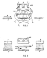
- FIG. 1 schematically shows an arrangement for producing a magneto-optical layer on substrates 3, 4, 5, which are guided past a sputter cathode in the form of a target 1 in the direction of arrow A.
- an aperture 2 with an opening 6 which, as will be explained in more detail later, can be designed asymmetrically with respect to the center of the sputter cathode or the target 1 .
- the target 1 has a composition of at least one element of the rare earth metals SE and at least one transition metal ÜM.
- Rare earth metals are generally terbium, gadolinium and dysprosium, while the transition metals are mainly iron and cobalt.
- the target alloy can include consist of terbium, gadolinium, dysprosium, iron and cobalt.
- a target alloy made of terbium, dysprosium, iron and cobalt or made of terbium, gadolinium, dysprosium and cobalt can be used.
- a composition of terbium, dysprosium and cobalt can also be used as the ternary alloy for target 1.
- the formula has a quantitative composition of the target alloy, for example (Tb x Dy 1-x ) y (Fe z Co 1-z ) 1-y With 0 ⁇ x ⁇ 1, 0.15 ⁇ y ⁇ 0.30 and 0.60 ⁇ z ⁇ 1.
- the target 1 is operated, for example, as a magnetron sputter cathode in a magnetron sputtering method known per se.
- the heart of the magnetron sputter cathode is a magnet system in which magnets with alternating poles are arranged on a soft iron plate.
- a section through such a planar magnetron MDC is shown schematically in FIGS. 1 and 2.
- the magnetron is electrically connected as the cathode, the substrate holder as the anode or at floating potential.
- the magnet arranged behind the target forms an inhomogeneous magnetic field below the target 1, which in combination with the electric field leads to a preferred removal of the target on the sputter trenches 9, 10 identified in FIG. 1.
- the rare earth metals and the PM are removed in such a different way that the different spatial distributions k1, k2, k3, k4 indicated in FIG. 1 occur for the rare earth metal and the transition metals.
- These different spatial distributions, also referred to as sputtering lobes, of the rare earth metals and the transition metals are exploited to in the dynamic magnetron sputter with only one cathode or only one target to obtain a specific concentration profile for the rare earth metals over the depth of the magneto-optical layer.
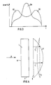
- FIG. 3 These depth profiles of the rare earth metals SE and the transition metals UM are shown in FIG. 3, in which the depth t of the magneto-optical layer is plotted on the axis of abscissa and the atomic percentages of the alloy components on the axis of ordinate.
- the target 1 in FIG. 1 consists of a terbium-iron-cobalt alloy
- terbium is distributed according to the sputtering lobes K1 and k4 in FIG. 1 and the transition metals iron plus cobalt according to the middle sputtering lobes k2 and k3.
- a magneto-optical layer which has an "M" -shaped terbium concentration profile with two peaks, as can be seen from the rare earth metal profile SE in FIG. 3, while the transition metal profile UM has a single peak which, however, projects beyond the two peaks of the terbium concentration profile.
- the magneto-optical layer can also be produced by a direct voltage discharge in a diode or triode sputter system.
- a diode sputtering system for example, the substrate to be coated is connected as an anode, and the target forms the sputter cathode for this purpose.
- a plasma is obtained between the two electrodes in a carrier gas which is under a certain pressure by applying a voltage.
- the ions of the carrier gas accelerated in the electric field knock out Target that forms the cathode, molecules or atoms that are deposited on the substrate.
- the magnetron sputtering method is preferred to the diode sputtering method, since higher sputtering rates are achieved with reduced power compared to diode sputtering and the substrate is heated up much less because only a few electrons strike the substrate because they are caused by the magnetic field of the magnetron cathode get distracted.
- ternstroms are arranged in the sputtering chamber 3 sputtering cathodes side by side in a parallel plane to the direction of movement A of the substrates 3, 4 and 5 to be coated, the sputtering cathodes consisting of targets 7, 1, 8 with different alloy compositions of rare earth transition metals.
- targets 7 and 8 are operated using the diode sputtering method and target 1 using the magnetron sputtering method. It is also possible for all three targets to be operated using the diode or magnetron sputtering method.
- the layer thickness profiles ie the distribution of the alloy components
- the layer thickness profiles can also be adjusted by changing the gas flow and the sputtering power of the individual cathodes.
- the close spatial proximity of the sputter cathodes causes a continuous transition of the concentrations of the alloy components. Since a jump in concentration in the magneto-optical layer is thus avoided, diffusion effects which can occur when the magneto-optical layer is repeatedly written and erased, and the changes in the read / write properties associated therewith, compared to a structure composed of discrete layers, are reduced.
- More than three sputter cathodes can also be used, for example if at least one side of the magneto-optical layer is covered by a dielectric layer.
- the dielectric layers against moisture and / or oxygen described above can be used as the dielectric layer.
- the thickness of this dielectric layer is chosen to be approximately ⁇ / 4 ⁇ n on the side facing the substrate, with the wavelength ⁇ of a writing laser and the refractive index n of the dielectric layer.
- the first target in the running direction of the substrate has e.g. a higher content of transition metal, in particular a higher cobalt content, than the second target 7 seen in the direction of travel.
- transition metals in particular an increased cobalt concentration
- concentration of rare earth metals is increased on the side of the magneto-optical layer facing away from the substrate.
- a layer of SiN, SiON, SiAlON, AlN, AlON, TaO x or NbO x with the refractive index results as a barrier layer or anti-reflection layer on the side of the magneto-optical layer facing the substrate n of the layer.
- the thickness of the barrier layer is less than / equal to the thickness of the barrier layer facing the substrate.
- the thickness of the magneto-optical layer is 15 to 100 nm.
- a characteristic layer structure is: substrate / 70nm ⁇ 5nm (Si, N) / 80nm ⁇ 5nmTbFeCo / 50nm ⁇ 5nm (Si, N), with a refractive index n of the silicon nitride of the first (Si , N) layer of 2.20 ⁇ 0.1 and the second (Si, N) layer of 2.05 ⁇ 0.05.
- the barrier layer on the substrate facing away from the magneto-optical layer is, for example, a reflection layer made of Al, Ag, Cu, Au, TiN or ZrN.
- Such a three-layer structure looks for example as follows: substrate / 70nm ⁇ 5nm (Si, N) / 25nm ⁇ 5nmTbFeCo / 50nm ⁇ 5nm reflection layer.
- a four-layer structure is also possible in which a reflective layer is applied to the barrier layer that faces away from the substrate.
- targets are sputtered which lie in front of the target 7 or behind the target 8 in FIG. 2.
- the target, not shown, lying in front of the target 7 consists, for example, of silicon, silicon-aluminum, aluminum, tantalum or niobium.
- the diode sputtering process or preferably the magnetron sputtering process is used in an argon and oxygen and / or nitrogen atmosphere.
- An SiN, SiON, SiAlON, AlN, AlON, TaO x or NbO x layer first forms on the substrate 3 as a barrier layer against moisture and / or oxygen.
- the corrosion resistance of the resulting magneto-optical recording medium is increased on the substrate 3, which is provided with such a barrier layer, by the cathode lying in the running direction or web direction A of the substrates in front of the magnetron sputter cathode, namely the target 7 corrosion-reducing ele sputtered in greater concentration.
- the target 7 can, for example, also consist entirely of a corrosion-preventing element, which is titanium, chromium, aluminum, platinum, zirconium, vanadium, tantalum, molybdenum, tungsten, copper, ruthenium, rhenium, palladium, silicon, niobium, iridium and / or hafnium.
- the target 7 can also contain two or more of these elements in higher concentration or consist entirely of two or more of these elements.
- the magneto-optical layer is then sputtered on, as is described with reference to FIG. 1.
- a corrosion-reducing element is sputtered on from a target 8, which has the same composition as the target 7.
- the corrosion-preventing element or elements have a higher concentration after sputtering in comparison to the average element concentration.
- the targets 7, 1, 8 in FIG. 2 are approximately at a distance from one another which corresponds to the distance from the targets to the substrates to be coated. This can result in an overlap of the sputtering lobes and layers with any concentration distribution in the layer depth can be produced.
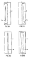
- this has an asymmetrical concentration gradient over the depth between the plane of the substrates and the targets, the diaphragm shown schematically in FIG. 5A or 5B, which has an aperture 6A or 6B, which is asymmetrical with respect to the center of the sputtering target or the sputtering cathode .
- FIGS. 5A to 5D show different embodiments of such an aperture 2, the aperture according to FIGS. 5C and 5D having an aperture 6c or 6d that runs symmetrically to the center line.
- curve S over a reference line g shows the sputtering rate for an element, for example a rare earth metal SE, which is applied to the substrate without an interposed aperture.
- the values r1, r2 are entered to represent the individual local sputter rate.
- a sputter rate according to curve C is obtained for the transition metals UM, the shape of which is changed compared to the shape for the rare earth metals SE.
- the target 1 from which sputtering has the width b perpendicular to the direction of movement A and the length 1 in the direction of movement A of the substrates.
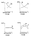
- the curves according to FIGS. 6A to 6D show the concentrations in atomic% of the transition metals UM and the rare earth metals SE over the layer depth of the magneto-optical layer.
- the substrate surface is marked on the t-axis in all four FIGS. 6A to 6D.
- FIG. 6B are mirror images of the curves in FIG. 6A, and the diaphragm in FIG. 5B is also mirror images of the diaphragm in FIG. 5A.
- FIG. 6C both the rare earth and the transition metals show an almost identical, constant concentration over the layer depth, while the course of the curves in FIG. 6D largely corresponds to the course of the curves according to FIG. 3.
- FIG. 7 shows schematically the coercive field strength H c and the compensation temperature T comp over the temperature T of a known magneto-optical layer and a layer according to the invention.
- the compensation temperature T comp becomes one magneto-optical layer or alloy obtained through the intersection of the two straight lines 1 / H c , which are determined from the curves H c (T) on both sides of the ordinate of the maximum coercive field strength.
- the coercive field strength for the layer according to the invention is designated H c inh
- the coercive field strength for the known magneto-optical layer is H c h
- the superscript indices "h” and "inh” stand for homogeneous and inhomogeneous composition of the respective alloy, although it should be noted that the inhomogeneous magneto-optical layer according to the invention has on average the same composition as the known homogeneous magneto-optical layer.
- the difference ⁇ T T 8kOe2 - T 8kOe1 is equal to or more than 100 ° C. in the material according to the invention, which is equivalent to the fact that the material properties are less sensitive to fluctuations in the material composition than those of homogeneous materials.
- the magnetic properties of the magneto-optical layer according to the invention differ significantly from the double layer, as described, for example, with reference to FIG. 3 of EP-A2 0 225 141.
- the magneto-optical layer according to the invention has only a single hysteresis loop during magnetization, in contrast to the double layer in the prior art, which shows two separate hysteresis loops, at the same time the magnetic properties of the magneto-optical layer according to the invention are far less dependent on the alloy composition.
Landscapes
- Engineering & Computer Science (AREA)
- Power Engineering (AREA)
- Chemical & Material Sciences (AREA)
- Nanotechnology (AREA)
- Manufacturing & Machinery (AREA)
- Crystallography & Structural Chemistry (AREA)
- Thin Magnetic Films (AREA)
- Physical Vapour Deposition (AREA)
- Crystals, And After-Treatments Of Crystals (AREA)
- Measuring Magnetic Variables (AREA)
- Magnetic Heads (AREA)
Abstract
Description
- Die Erfindung betrifft eine magnetooptische Schicht aus einer amorphen Seltenerd-Übergangsmetall-Legierung mit einer magnetischen Anisotropie, deren leicht magnetisierbare Achse senkrecht zu der Oberfläche steht.
- Amorphe magnetooptische Materialien mit einer solchen uniaxialen senkrechten Anisotropie sind bekannt. Am meisten verbreitet sind Legierungen von Seltenerdmetallen wie Gadolinium, Terbium, Dysprosium, mit Übergangsmetallen, wie Eisen und Kobalt, denen gegebenenfalls noch weitere Komponenten zugesetzt sind. Die magnetischen Eigenschaften dieser Legierungen hängen sehr stark von ihrer Zusammensetzung ab.
- In der DE-OS 33 09 483 sind magnetooptische Aufzeichnungsmaterialien aus amorphen ternären Legierungen auf der Basis von Terbium, Eisen und Kobalt beschrieben, die für Kobaltanteile ≦ 40 % einen näherungsweise linearen Zusammenhang des Winkels der Kerr-Drehung und der Curie-Temperatur mit dem Kobaltgehalt der Legierungen zeigen. Das gleiche gilt für die magnetooptischen Aufzeichnungsmedien, die in der DE-OS 35 36 210 und der Zeitschrift "Journal of Applied Physics", 64 (1988), S. 262, beschrieben sind. So ist aus der DE-OS 35 36 210 ein magnetooptisches Aufzeichnungsmedium aus einem amorphen Film der Zusammensetzung Seltenerd-Übergangsmetalle mit einer Kompensationstemperatur von 50 bis 200 °C oder einer solchen von 0 °C oder weniger bekannt. Bei Verwendung eines amorphen Films des Tb-Fe-Co-Systems wird die Kompensationstemperatur von 50 bis 200 °C durch eine Zusammensetzung mit 24 bis 30 Atomprozent Terbium, 7 bis 20 Atomprozent Kobalt, Rest Eisen, erreicht, während eine Kompensationstemperatur von 0 °C oder weniger durch eine Zusammensetzung mit 18 bis 21,5 Atomprozent Terbium, 8 bis 10 Atomprozent Kobalt und dem Rest Eisen erzielt wird. Diese Zusammenhänge sind in der Offenlegungsschrift DE 35 36 210 ausführlich erläutert.
- In den Zeitschriften "Journal of Applied Physics", 61 (1987), ab Seite 2610, und "J. Vac. Sci. Technol. A5 (1987), ab Seite 1949 wird darauf hingewiesen, daß beispielsweise die Erhöhung des Terbiumgehalts um 1 Atomprozent die Kompensationstemperatur bis zu 40 °C verschieben kann.
- Die Kontrolle der Zusammensetzung der Schicht ist daher sehr wichtig für die Auslegung des Sputtervorgangs und einer entsprechenden Produktionsanlage, wie aus der Zeitschrift "Solid State Technology", März 1988, S. 107, hervorgeht.
- Im allgemeinen wird angegeben, daß die Abweichung der Tb-Konzentration von der mittleren Konzentration im Schichtvolumen weniger als 0,5 % betragen soll.
- Die angestrebte Gleichmäßigkeit der Zusammensetzung der Legierungsbestandteile im Tiefenprofil einer magnetooptischen Aufzeichnungsschicht sowie die Bemühungen, die Legierungszusammensetzung über die Beschichtungsbreite und -länge konstant zu halten, erfordern einen großen Aufwand, z.B. rotieren die zu beschichtenden Platten während des Beschichtungsvorgangs um ihre eigene Drehachse und laufen gleichzeitig auf einem größeren Kreis um.
- Ein weiterer Nachteil bekannter magnetooptischer Aufzeichnungsmaterialien ist ihre große Korrosionsanfälligkeit.
- Zur Vermeidung bzw. Verhinderung dieses Nachteils wird der Zusatz verschiedener korrosionsverhindernder Elemente zu den magnetooptischen Legierungen empfohlen (GB-A - 2.175.160 und EP-A1 - 0 229 292). Der Zusatz derartiger Elemente zum Gesamtvolumen der magnetooptischen Aufzeichnungsschicht verbessert die Korrosionsbeständigkeit, jedoch zu Lasten anderer erwünschter Eigenschaften, wie die eines möglichst großen Kerr-Winkels, einer hohen Koerzitivfeldstärke, hoher Schreibempfindlichkeit, großen Signal-zu-Rausch-Verhältnisses und dergleichen. Bei dem magnetooptischen Aufzeichnumgsmedium gemäß der EP-A1 - 0 229 292 werden zu einem ersten Element weitere korrosionsverhindernde Elemente zugesetzt, um eine Anreicherung der korrosionsverhindernden Elemente an der Oberfläche des Aufzeichnungsmediums zu erreichen. Dabei ist nachteilig, daß durch den Zusatz weiterer Elemente die erwünschten magneto optischen Eigenschaften noch stärker beeinträchtigt werden können.
- In der US-PS 4 740, 430 sind dünne Barriereschichten aus korrosionsverhindernden Elementen beschrieben. Dabei handelt es sich um eine diskrete, mehrlagige Struktur des magnetooptischen Aufzeichnungsmediums.
- Um eine hohe Speicherdichte der magnetooptischen Aufzeichnungsmaterialien zu erreichen, müssen stabile, möglichst kleine Domänen in der magnetooptischen Aufzeichnungsschicht erzeugt werden können. Voraussetzung hierfür ist es, daß das Produkt aus Sättigungsmagnetisierung Ms und Koerzitivfeldstärke Hc möglichst groß ist (Kryder et al., SPIE Proc. 420, S. 236 (1983)). Für bekannte magnetooptische Aufzeichnungsmaterialien wird ein möglichst großes Produkt aus Sättigungsmagnetisierung und Koerzitivfeldstärke nur in einem engen Temperaturbereich um die Kompensationstemperatur Tcomp erreicht.
- In neuerer Zeit wurden magnetooptische Aufzeichnungsmaterialien beschrieben, die sich für das direkte Überschreiben der Information eignen (US-PS 4,694,358, US-PS 4,649,519, EP-A2 - 0 225 141, EP-A2 - 0 227 480 und EP-A2 - 0 217 096). In allen Fällen wird ein Aufbau des magnetooptischen Aufzeichnungsmediums verwendet, bei dem zwei getrennte Schichten mit unterschiedlichen magnetischen Eigenschaften übereinander geschichtet sind.
- In den Druckschiften EP-A2 - 0 217 096 und EP-A2 - 0 227 480 sind magnetooptische Aufzeichnungsmedien beschrieben, bei denen eine thermisch isolierende Zwischenschicht zwischen der magnetooptischen Aufzeichnungsschicht und einer magnetischen Schicht, die ein Vormagnetisierungsfeld erzeugt, im Aufbau vorhanden ist. In den übrigen, voranstehend erwähnten Literaturstellen werden solche Zwischenschichten empfohlen, da es anderenfalls zur Diffusion von Legierungskomponenten in die Magnetschicht kommen kann. Eine derartige Diffusion von Legierungskomponenten ändert selbstverständlich die Eigenschaften des magnetooptischen Aufzeichnungsmediums.
- Ein anderer Weg zur Erhöhung der Langzeitstabilität eines magnetooptischen Speichers wird in dem Verfahren gemäß der DE-OS 36 42 161 vorgeschlagen, bei dem während und/oder nach der Abscheidung einer dieleketrischen Schicht, einer magnetooptischen Schicht sowie einer Deckschicht nacheinander auf einem Substrat in nahezu trockener Atmosphäre in einem Temperaturbereich von Raumtemperatur bis knapp unterhalb der Kristallisationstemperatur der magnetooptischen Schicht getempert wird.
- Aus der japanischen Offenlegungsschrift 188,843/88 ist ein Verfahren zum Herstellen einer fotomagnetischen Platte bekannt, bei der die fotomagnetische Aufzeichnungsschicht in der Weise aufgesputtert wird, daß das Substrat an drei Targets aus Seltenerdmetall und Übergangsmetall vorbeigeführt wird. Das mittlere Target ist parallel zu der Bewegungsbahn des Substrats angeordnet, während jeweils ein Target vor und hinter dem mittleren Target in Bewegungsrichtung des Substrats unter einem vorgegebenen Winkel gegenüber dem mittleren Target angebracht ist. Die Zusammensetzung des so erhaltenen fotomagnetischen Aufzeichnungsfilms auf dem Substrat ist gleichmäßig.
- Aufgabe der Erfindung ist es, eine magnetooptische Schicht der eingangs beschriebenen Art zu schaffen, die einfach und reproduzierbar herstellbar ist, eine hohe Korrosionsbeständigkeit gegenüber Feuchtigkeit und/oder Sauerstoff besitzt, hohe Speicherdichten ermöglicht und für das direkte Überschreiben geeignet ist. Im Rahmen dieser Aufgabe soll auch ein Herstellungsverfahren für eine derartige magnetooptische Schicht geschaffen werden.
- Diese Aufgabe wird erfindungsgemäß dadurch gelöst, daß die magnetooptische Schicht einen Gradienten der Konzentration der Zusammensetzung über der Tiefe aufweist und in einem Temperaturbereich von ΔT = 100 °C um die Kompensationstemperatur Tcomp herum eine Koerzitivfeldstärke von größer als 8 kOe besitzt.
- In Ausgestaltung der Erfindung besteht die Legierung aus Terbium, Gadolinium, Dysprosium, Eisen und Kobalt oder aus Terbium, Dysprosium, Eisen und Kobalt. Desweiteren kann die Legierung aus Terbium, Gadolinium, Dysprosium und Kobalt oder aus Terbium, Dysprosium und Kobalt allein bestehen. Zweckmäßigerweise hat die eine der Legierungen der magnetooptischen Schicht eine Zusammensetzung nach der Formel
(TbxDy1-x)y (FezCo1-z)1-y
mit
0 ≦ x ≦ 1,
0,15 ≦ y ≦ 0,30
und 0,60 ≦ z ≦ 1. - In Weiterbildung der Erfindung befindet sich in einer oder beiden Oberflächen der magnetooptischen Schicht eine gegenüber der durchschnittlichen Konzentration der Zusammensetzung erhöhte Konzentration an Seltenerdmetallen.
- Ebenso ist es möglich, daß sich in einer oder beiden Oberflächen der magnetooptischen Schicht eine gegenüber der durchschnittlichen Konzentration erhöhte Konzentration an Übergangsmetallen befindet.
- Die weitere Ausgestaltung der magnetooptischen Schicht ergibt sich aus den Merkmalen der Patentansprüche 9 bis 12.
- Eine magnetooptische Schicht nach der Erfindung ist Bestandteil eines magnetooptischen Aufzeichnungsmediums, bei dem die magnetooptische Schicht zwischen zwei Sperrschichten aus SiN, SiON, SiAlON, AlN, AlON, TaOx oder NbOx zum Schutz gegen Feuchtigkeit und/oder Sauerstoff angeordnet ist. Die eine Sperrschicht ist einseitig von einem Substrat, die andere von einem Metallspiegel, einer Lack- oder einer Kleberschicht und einem zweiten Substrat abgedeckt.
- Das Verfahren zur Herstellung einer magnetooptischen Schicht zeichnet sich dadurch aus, daß das Aufsputtern der Seltenerd-Übergangsmetall-Legierung dynamisch erfolgt, indem das zu beschichtende Substrat relativ zu einem oder mehreren Sputtertargets bewegt wird, die in einer gemeinsamen Ebene angeordnet sind.
- Die weiteren Verfahrensmaßnahmen zum Herstellen der magnetooptischen Schicht ergeben sich aus den Merkmalen der Patentansprüche 17 bis 35.
- Die magnetooptischen Schichten nach der Erfindung finden Verwendung für ein direkt überschreibbares magnetooptisches Aufzeichnungsmedium und in einem System, in dem eine Modulation des magnetischen Feldes oder eine Modulation der Laserenergie während des Einschreibens der Information erfolgt.
- Die Erfindung wird im folgenden anhand der Zeichnungen näher erläutert. Es zeigen:
- Figur 1 in schematischer Darstellung die Anordnung eines Targets in einer Ebene parallel zu der Bahn von zu beschichtenden Substraten,
- Figur 2 eine schematische Anordnung von mehreren Tar gets in einer gemeinsamen Parallelebene zu der Bahn der zu beschichtenden Substrate,
- Figur 3 schematisch die Zusammensetzung einer magnetooptischen Schicht auf der Basis Seltenerdmetalle SE und Übergangsmetalle ÜM über der Tiefe der Schicht,
- Figur 4 die Blendencharakteristik einer zwischen Targets und Substrat zwischengeschalteten Blende und die Sputterraten über der Tiefe der magnetooptischen Schicht,
- Figuren 5A bis 5D eine Draufsicht auf verschiedene Blenden mit unterschiedlichen Blendenöffnungen, die zwischen den Targets und den Substraten angeordnet sind,
- Figuren 6A bis 6D schematisch die Zusammensetzung von magnetooptischen Schichten über den Schichttiefen, die mit den Blenden gemäß den Figuren 5A bis 5D erhalten werden,
- Figur 7 den Zusammenhang zwischen der Koerzitivfeldstärke Hc und der Temperatur T verschiedener magnetooptischen Schichten, und
- Figur 8 den Zusammenhang zwischen dem Kehrwert 1/Hc der Koerzitivfeldstärke und der Temperatur T der magnetooptischen Schichten nach Fig. 7.
- In Figur 1 ist schematisch eine Anordnung zum Herstellen einer magnetooptischen Schicht auf Substraten 3, 4, 5 dargestellt, die in Richtung des Pfeils A an einer Sputterkathode in Gestalt eines Targets 1 vorbeigeführt werden. Zwischen dem Target 1 und der Bahnebene der Substrate 3, 4, 5 befindet sich eine Blende 2 mit einer Öffnung 6, die, wie später noch näher ausgeführt werden wird, in bezug auf die Mitte der Sputterkathode bzw. des Targets 1 unsymmetrisch ausgebildet sein kann.
- Das Target 1 hat eine Zusammensetzung aus zumindest einem Element der Seltenerdmetalle SE und zumindest einem Übergangsmetall ÜM. Bei den Seltenerdmetallen handelt es sich im allgemeinen um Terbium, Gadolinium und Dysprosium, während die Übergangsmetalle vor allem Eisen und Kobalt sind. Die Targetlegierung kann u.a. aus Terbium, Gadolinium, Dysprosium, Eisen und Kobalt bestehen. Desweiteren ist eine Targetlegierung aus Terbium, Dysprosium, Eisen und Kobalt oder aus Terbium, Gadolinium, Dysprosium und Kobalt verwendbar. Als ternäre Legierung für das Target 1 kommt auch eine Zusammensetzung aus Terbium, Dysprosium und Kobalt in Frage.
- Eine quantitative Zusammensetzung der Targetlegierung hat beispielsweise die Formel
(TbxDy1-x)y(FezCo1-z)1-y
mit
0 ≦ x ≦ 1,
0,15 ≦ y ≦ 0,30
und 0,60 ≦ z ≦ 1. - Es ergibt sich u.a. für eine ternäre Legierung, die als einziges Element der Seltenerdmetalle Terbium enthält, eine bevorzugte Zusammensetzung, wie Tb0,22-0,28 Fe0,70-0,64 Co0,08 des Sputtertargets.
- Das Target 1 wird beispielsweise als Magnetron-Sputter-Kathode in einem an sich bekannten Magnetron-Sputter-Verfahren betrieben. Das Kernstück der Magnetron-Sputter-Kathode ist ein Magnetsystem, bei dem auf einer Weicheisenplatte Magnete mit wechselnden Polen angeordnet sind. EIn Schnitt durch ein derartiges Planarmagnetron MDC ist schematisch in den Figuren 1 und 2 dargestellt. Elektrisch ist das Magnetron als Kathode geschaltet, der Substrathalter als Anode oder auf floatendem Potential. Zwischen den Elektroden befindet sich ein ionisiertes Gas, beispielsweise aus Argon, das unter einem bestimmten Druck, vorzugsweise 3·10⁻³ mbar bis 2·10⁻² mbar steht. Durch den hinter dem Target angeordneten Magneten bildet sich ein inhomogenes Magnetfeld unterhalb des Targets 1 aus, das in Kombination mit dem elektrischen Feld zu einem bevorzugten Abtrag des Targets an den in Fig. 1 gekennzeichneten Sputtergräben 9, 10 führt. Darüberhinaus werden die SE-Metalle und die ÜM derart unterschiedlich abgetragen, daß die in Fig. 1 angedeuteten unterschiedlichen räumlichen Verteilungen k1, k2, k3, k4 für das Seltenerdmetall und die Übergangsmetalle auftreten. Diese unterschiedlichen räumlichen Verteilungen, weiterhin als Sputterkeulen bezeichnet, der Seltenerdmetalle und der Übergangsmetalle werden ausgenutzt, um im dynamischen Magnetron sputtern mit nur einer Kathode bzw. nur einem Target ein bestimmtes Konzentrationsprofil für die Seltenerdmetalle über der Tiefe der magnetooptischen Schicht zu erhalten. Diese Tiefenprofile der Seltenerdmetalle SE und der Übergangsmetalle ÜM sind in Figur 3 dargestellt, in der auf der Abszissenachse die Tiefe t der magnetooptischen Schicht und auf der Ordinatenachse die Atomprozente der Legierungsbestandteile aufgetragen sind. Besteht beispielsweise das Target 1 in Figur 1 aus einer Terbium-Eisen-Kobalt-Legierung, so verteilt sich Terbium gemäß den Sputterkeulen K1 und k4 in Figur 1 und die Übergangsmetalle Eisen plus Kobalt gemäß den mittleren Sputterkeulen k2 und k3. Es wird somit eine magnetooptische Schicht erhalten, die ein "M"-förmiges Terbiumkonzentrationsprofil mit zwei Spitzen erhält, wie aus dem Seltenerdmetallprofil SE in Figur 3 ersichtlich ist, während das Übergangsmetallprofil ÜM eine einzige Spitze aufweist, die jedoch die beiden Spitzen des Terbiumkonzentrationsprofils überragt.
- Selbstverständlich kann die magnetooptische Schicht auch durch eine Gleichspannungsentladung in einer Dioden- oder Triodensputteranlage hergestellt werden. In einer derartigen Diodensputteranlage ist beipsielsweise das zu beschichtende Substrat als Anode geschaltet, und das Target bildet hierzu die Sputterkathode. Zwischen den beiden Elektroden wird in einem Trägergas, das unter einem bestimmten Druck steht, durch Anlegen einer Spannung ein Plasma erhalten. Die im elektrischen Feld beschleunigten Ionen des Trägergases schlagen aus dem Target, das die Kathode bildet, Moleküle oder Atome heraus, die sich auf dem Substrat niederschlagen. Im allgemeinen wird das Magnetron-Sputter-Verfahren dem Diodensputterverfahren vorgezogen, da höhere Sputterraten bei verringerter Leistung im Vergleich zum Diodensputtern erzielt werden und eine weit geringere Aufheizung der Substrate auftritt, da nur wenige Elektronen auf das Substrat auftreffen, weil diese durch das Magnetfeld der Magnetronkathode abgelenkt werden.
- Durch die unterschiedlichen Sputterkeulen für Seltenerdmetalle und Übergangsmetalle findet sich in der Mitte der magnetooptischen Schicht eine gegenüber der durchschnittlichen Konzentration erhöhte Konzentration an Übergangsmetallen. Desweiteren gilt, daß sich an den Rändern in einer oder beiden Oberflächen der magnetooptischen Schicht eine gegenüber der durchschnittlichen Konzentration erhöhte Konzentration an Seltenerdmetallen befindet. Aus Fig. 3 ist ersichtlich, daß durch geeignete Auslegung der in den Fig. 5A bis 5D beispielhaft skizzierten Blenden, die zwischen der Kathode und dem Substrat angebracht werden, erreicht wird, daß ein M-förmiges Profil der SE Konzentration, einΛ-förmiges und ein V-förmiges Profil der SE Konzentration auftreten kann. Ebenso ist es möglich, durch geeignetes Hintereinanderschalten von Beschichtungsstationen mit überlappenden Sputterkeulen praktisch jede Art von Konzentrationsverteilungen in der Tiefe einzustellen.
- In der in Figur 2 gezeigten Ausführungsform einer Sput ternanlage sind in der Sputterkammer 3 Sputterkathoden nebeneinander in einer Parallelebene zu der Bewegungsrichtung A der zu beschichtenden Substrate 3, 4 und 5 angeordnet, wobei die Sputterkathoden aus Targets 7, 1, 8 mit unterschiedlichen Legierungszusammensetzungen aus Seltenerd-Übergangsmetallen bestehen. Beispielsweise werden die Targets 7 und 8 nach dem Dioden-Sputterverfahren und das Target 1 nach dem Magnetron-Sputterverfahren betrieben. Ebenso ist es möglich, daß alle drei Targets nach dem Dioden- bzw. nach dem Magnetron-Sputterverfahren betrieben werden. Durch Verändern des Gasflusses und der Sputterleistung der einzelnen Kathoden lassen sich im im Falle des Magnetron-Sputterverfahrens die Schichtdickenprofile, d.h. die Verteilung der Legierungsbestandteile, ebenfalls einstellen. Die enge räumliche Nähe der Sputterkathoden bewirkt einen kontinuierlichen Übergang der Konzentrationen der Legierungsbestandteile. Da somit ein Konzentrationssprung in der magnetooptischen Schicht vermieden wird, sind Diffusionseffekte, die beim wiederholden Schreiben und Löschen der magnetooptischen Schicht auftreten können, und damit verbundene Veränderungen der Schreib/Leseeigenschaften, gegenüber einem Aufbau aus diskreten Lagen, reduziert.
- Es können auch mehr als drei Sputterkathoden eingesetzt werden, beispielsweise dann, wenn mindestens eine Seite der magnetooptischen Schicht von einer dielektrischen Schicht abgedeckt wird. Als dieleketrische Schicht kommen u.a. die voranstehend beschriebenen Sperrschichten gegen Feuchtigkeit und/oder Sauerstoff in Frage. Die Dicke dieser dielektrischen Schicht wird auf der dem Substrat zugewandten Seite ungefähr λ/4 · n gewählt, mit der Wellenlänge λ eines Schreiblasers und dem Brechungsindex n der dielektrischen Schicht.
- Das in Laufrichtung des Substrats erste Target weist z.B. einen höheren Gehalt an Übergangsmetall, insbesondere, einen höheren Kobaltgehalt, auf als das, in Laufrichtung gesehen, zweite Target 7.
- Auf der dem Substrat zugewandten Seite der magnetooptischen Schicht befindet sich beipielsweise eine erhöhte Konzentration von Übergangsmetallen, insbesondere eine erhöhte Kobaltkonzentration, während auf der vom Substrat abgewandten Seite der magnetooptischen Schicht die Konzentration an Seltenerdmetallen erhöht ist.
- Als Sperrschicht oder Antireflexionsschicht auf der dem Substrat zugewandten Seite der magnetooptischen Schicht ergibt sich nach dem Sputtern eine Schicht aus SiN, SiON, SiAlON, AlN, AlON, TaOx oder NbOx, die eine Dicke von etwa λ/4n hat, mit dem Brechungsindex n der Schicht. Auf der vom Substrat abgewandten Seite der magnetooptischen Schicht ist die Dicke der Sperrschicht kleiner/gleich der Dicke der substratzugewandten Sperrschicht. Die Dicke der magnetooptischen Schicht beträgt 15 bis 100 nm. Ein characteristischer Schichtaufbau lautet: Substrat/70nm±5nm(Si,N)/80nm±5nmTbFeCo/50nm±5nm(Si,N), mit einem Brechungsindex n des Siliziumnitrids der ersten (Si,N)-Schicht von 2,20±0,1 und der zweiten (Si,N)-Schicht von 2,05±0,05. Die Sperrschicht auf der substrat abgewandten Seite der magnetooptischen Schicht ist z.B. eine Reflexionsschicht aus Al, Ag, Cu, Au, TiN oder ZrN. Ein derartiger Dreischichtaufbau sieht beispielsweise so aus: Substrat/70nm±5nm(Si,N)/25nm±5nmTbFeCo/50nm±5nm Reflexionsschicht. Es ist außer diesen Dreischichtaufbauten auch ein Vierschichtaufbau möglich, bei dem auf der Sperrschicht, die substratabgewandt ist, eine Reflexionsschicht aufgebracht ist.
- Werden Sperrschichten auf beiden Seiten des magnetooptischen Aufzeichnungsmediums aufgebracht, so wird von Targets gesputtert, die vor dem Target 7 bzw. hinter dem Target 8 in Fig. 2 liegen. Dabei besteht das vor dem Target 7 liegende, nicht gezeigte Target beispielsweise aus Silizium, Silizium-Aluminium, Aluminium, Tantal oder Niob. Es wird das Diodensputterverfahren oder bevorzugt das Magnetron-Sputterverfahren in einer Argon- und Sauerstoff- und/oder Stickstoffatmosphäre angewandt. Auf dem Substrat 3 bildet sich zuerst eine SiN-, SiON-, SiAlON-, AlN-, AlON-, TaOx- oder NbOx-Schicht als Sperrschicht gegen Feuchtigkeit und/oder Sauerstoff aus.
- Im darauffolgenden Verfahrensschritt wird auf dem Substrat 3, das mit einer derartigen Sperrschicht versehen ist, die Korrosionsbeständigkeit des entstehenden magnetooptischen Aufzeichnungsmediums erhöht, indem von der in Laufrichtung bzw. Bahnrichtung A der Substrate vor der Magnetron-Sputterkathode liegenden Kathode, nämlich dem Target 7, ein korrosionsverminderndes Ele ment in größerer Konzentration aufgesputtert wird. Das Target 7 kann beispielsweise auch vollständig aus einem korrosionsverhindernden Element bestehen, bei dem es sich um Titan, Chrom, Aluminium, Platin, Zirkonium, Vanadium, Tantal, Molybdän, Wolfram, Kupfer, Ruthenium, Rhenium, Palladium, Silizium, Niob, Iridium und/oder Hafnium handeln kann. Das Target 7 kann auch zwei oder mehrere dieser Elemente in höherer Konzentration enthalten oder zur Gänze aus zwei oder mehreren dieser Elemente bestehen. Im Anschluß daran wird die magnetooptische Schicht aufgesputtert, wie sie anhand von Fig. 1 beschrieben ist. Im letzten Verfahrensschritt wird von einem Target 8 aus, das die gleiche Zusammensetzung wie das Target 7 hat, ein korrosionsverminderndes Element aufgesputtert. In einer oder beiden Oberflächen der magnetooptischen Schicht weisen das bzw. die korrosionsverhindernden Elemente nach dem Sputtern eine höhere Konzentration im Vergleich zu der durchschnittlichen Elementenkonzentration auf.
- Die Targets 7, 1, 8 in Figur 2 haben untereinander etwa einen Abstand, der dem Abstand der Targets zu den zu beschichtenden Substraten entspricht. Dadurch kann es zu einem Überlappen der Sputterkeulen kommen und Schichten mit beliebiger Konzentrationsverteilung in der Schichttiefe hergestellt werden.
- Um in der magnetooptischen Schicht ein Tiefenprofil der Seltenerd- und Übergangsmetalle zu erhalten, das einen unsymmetrischen Konzentrationsgradienten über der Tiefe aufweist, kann, zwischen der Ebene der Substrate und den Targets, die in der Figur 5A oder 5B schematisch gezeigte Blende angeordnet werden, die eine Blendenöffnung 6A bzw. 6B aufweist, die in bezug auf die Mitte des Sputtertargets bzw. der Sputterkathode unsymmetrisch ausgebildet ist.
- Die Figuren 5A bis 5D zeigen verschiedene Ausführungsformen einer solchen Blende 2, wobei die Blende nach den Figuren 5C und 5D eine zur Mittellinie symmetrisch verlaufende Blendenöffnung 6c bzw. 6d besitzt.
- In Figur 4 zeigt die Kurve S über einer Bezugslinie g die Sputterrate für ein Element, beispielsweise ein Seltenerdmetall SE an, das ohne zwischengeschaltete Blende auf das Substrat aufgebracht wird. Stellvertretend für die einzelne lokale Sputterrate sind die Werte r1, r2 eingetragen. Für die Übergangsmetalle ÜM wird eine Sputterrate gemäß der Kurve C erhalten, deren Form gegenüber der Form für die Seltenerdmetalle SE verändert ist. Das Target 1, von dem aus gesputtert wird, hat die Breite b senkrecht zur Bewegungsrichtung A und die Länge 1 in Bewegungsrichtung A der Substrate.
- Die Kurven gemäß den Figuren 6A bis 6D geben die Konzentrationen in Atom % der Übergangsmetalle ÜM und der Seltenerdmetalle SE über der Schichttiefe der magnetooptischen Schicht wieder. In allen vier Figuren 6A bis 6D ist die Substratoberfläche auf der t-Achse markiert.
- Diese Kurven werden durch Zwischenschalten der in den Fig. 5A bis 5D gezeigten Blenden zwischen dem oder den Sputtertargets und dem Substrat erhalten, wobei der jeweiligen Blende, die in den Figuren 5A bis 5D gezeigt ist, die jeweiligen Kurven gemäß den Figuren 6A bis 6D zugeordnet sind, d.h. mit der Blende 2 in Figur 5A korrespondieren die beiden Kurven in Fig. 6A, mit der Blende 2 in Fig. 5B werden die beiden Kurven der Fig. 6B erhalten und so fort. In Fig. 6A ist die Konzentration der Seltenerdmetalle SE an der Substratoberfläche am größten und nimmt mit der Schichttiefe t ab, während die Konzentration der Übergangsmetalle ÜM ab einer bestimmten Schichttiefe allmählich ansteigt. Die Kurven für die Seltenerdmetalle SE und die Übergangsmetalle ÜM in Fig. 6B verhalten sich spiegelbildlich zu den Kurven in Fig. 6A, ebenso ist die Blende in Fig. 5B zur Blende in Fig. 5A spiegelbildlich angeordnet. In Fig. 6C zeigen sowohl die Seltenerd- als auch die Übergangsmetalle eine nahezu gleiche, konstante Konzentration über die Schichttiefe, während der Verlauf der Kurven in Fig. 6D weitgehend dem Verlauf der Kurven gemäß Fig. 3 entspricht.
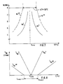
- In Figur 7 sind schematisch die Koerzitivfeldstärke Hc sowie die Kompensationstemperatur Tcomp über der Temperatur T einer bekannten magnetooptischen Schicht und einer Schicht nach der Erfindung dargestellt. Bei der Kompensationstemperatur Tcomp besitzt die Koerzitivfeldstärke Hc ein sehr ausgeprägtes Maximum. Im allgemeinen wird die Kompensationstemperatur Tcomp einer magnetooptischen Schicht bzw. Legierung durch den Schnittpunkt der beiden Geraden 1/Hc erhalten, die aus den Kurven Hc (T) beidseitig der Ordinate der maximalen Koerzitivfeldstärke bestimmt werden.
- Die Koerzitivfeldstärke für die Schicht nach der Erfindung ist mit Hc inh bezeichnet, während die Koerzitivfeldstärke für die bekannte magnetooptische Schicht Hc h lautet. Die hochgestellten Indizes "h" und "inh" stehen für homogene und inhomogene Zusammensetzung der jeweiligen legierung, wobei jedoch zu beachten ist, daß die inhomogene magnetooptische Schicht nach der Erfindung im Mittel die gleiche Zusammensetzung wie die bekannte homogene magnetooptische Schicht aufweist. Ab einer Koerzitivfeldstärke Hc gleich oder größer 8kOe wird ein Temperaturintervall
ΔT = T8kOe2 - T8kOe1 ≧ 100 °C
der Kompensationstemperaturen für die inhomogene Schichtzusammensetzung erhalten, wie anschließend anhand von Fig. 8 erläutert wird. - Aus Fig. 8 ist ersichtlich, daß das erfindungsgemäße Material eine Abhängigkeit 1/Hc inh(T) in Form zweier Strahlen aufweist, die, verglichen mit den Strahlen 1/Hc h (T) der bekannten Materialien wesentlich geringere Steigungen haben. Wird 1/Hc inh von hohen Temperaturen gegen 1/Hc inh = 0[1/k0e] extrapoliert, so ergibt sich eine Kompensationstemperatur Tcomp2, während eine Extrapolation von tiefen Temperaturen eine Kompensations temperatur Tcomp1 liefert. Bei den bekannten magnetooptischen Materialien wird für beide Extrapolationen dieselbe Kompensationstemperatur Tcomp erhalten.
- Der Unterschied ΔT = T8kOe2 - T8kOe1 beträgt bei dem erfindungsgemäßen Material gleich oder mehr als 100 °C, was gleichbedeutend damit ist, daß die Materialeigenschaften gegenüber Schwankungen in der Materialzusammensetzung weniger empfindlich sind als diejenigen von homogenen Materialien.
- Die magnetischen Eigenschaften unterscheiden sich bei der magnetooptischen Schicht nach der Erfindung erheblich von der Doppelschicht, wie sie beispielsweise anhand von Figur 3 der EP-A2 0 225 141 beschrieben ist. Die magnetooptische Schicht nach der Erfindung weist bei der Magnetisierung nur eine einzige Hystereseschleife auf, im Gegensatz zu der Doppelschicht im Stand der Technik, die zwei voneinander getrennte Hystereseschleifen zeigt, gleichzeitig sind die magnetischen Eigenschaften der erfindungsgemäßen magnetooptischen Schicht weit weniger stark von der Legierungszusammensetzung abhängig. Wird die durchschnittliche Terbiumkonzentration durch Röntgenfluoreszenzanalyse bestimmt und mit den Schreib-/Leseeigenschaften verglichen, so zeigen Schichten mit 20 Atomprozent Terbium im Rahmen der Meßgenauigkeit das gleiche Signal-zu-Rausch-Verhältnis und die gleichen Empfindlichkeitswerte wie Schichten mit 24 Atomprozent Terbium. Im Stand der Technik ist es bisher nicht bekannt, daß der Anteil des oder der Seltenerdmetalle in der Legierung in so weiten Grenzen schwanken kann, ohne daß sich dadurch die magnetischen Eigenschaften erheblich verändern.
Claims (35)
0 ≦ x ≦ 1
0,15 ≦ y ≦ 0,30
0,60 ≦ z ≦ 1.
(TbxDy1-x)y (FezCo1-z)1-y
mit
0 ≦ x ≦ 1
0,15 ≦ y ≦ 0,30
und 0,60 ≦ z ≦ 1
aufweist.
Tb0,22-0,28 Fe0,70-0,64 Co0,08
hat.
Applications Claiming Priority (2)
| Application Number | Priority Date | Filing Date | Title |
|---|---|---|---|
| DE3904611A DE3904611A1 (de) | 1989-02-16 | 1989-02-16 | Magnetooptische schicht und verfahren zu ihrer herstellung |
| DE3904611 | 1989-02-16 |
Publications (3)
| Publication Number | Publication Date |
|---|---|
| EP0383216A2 true EP0383216A2 (de) | 1990-08-22 |
| EP0383216A3 EP0383216A3 (de) | 1991-09-11 |
| EP0383216B1 EP0383216B1 (de) | 1995-11-08 |
Family
ID=6374184
Family Applications (1)
| Application Number | Title | Priority Date | Filing Date |
|---|---|---|---|
| EP90102647A Expired - Lifetime EP0383216B1 (de) | 1989-02-16 | 1990-02-10 | Magnetooptische Schicht und Verfahren zu ihrer Herstellung |
Country Status (12)
| Country | Link |
|---|---|
| US (1) | US5527605A (de) |
| EP (1) | EP0383216B1 (de) |
| JP (1) | JP2996681B2 (de) |
| AT (1) | ATE130117T1 (de) |
| AU (1) | AU630664B2 (de) |
| BR (1) | BR9000700A (de) |
| CA (1) | CA2010014A1 (de) |
| DE (2) | DE3904611A1 (de) |
| DK (1) | DK0383216T3 (de) |
| ES (1) | ES2081311T3 (de) |
| FI (1) | FI900721A7 (de) |
| ZA (1) | ZA901150B (de) |
Cited By (2)
| Publication number | Priority date | Publication date | Assignee | Title |
|---|---|---|---|---|
| EP0642126A3 (de) * | 1993-09-02 | 1995-03-15 | Fujitsu Limited | Magnetooptisches Aufzeichnungsmedium |
| EP0674310A1 (de) * | 1994-03-24 | 1995-09-27 | Sharp Kabushiki Kaisha | Magnetooptisches Aufzeichnungsmedium und Verfahren zu seiner Herstellung |
Families Citing this family (13)
| Publication number | Priority date | Publication date | Assignee | Title |
|---|---|---|---|---|
| DE69326525T2 (de) * | 1992-11-17 | 2000-01-27 | Mitsubishi Chemical Corp., Tokio/Tokyo | Magnetooptischer Aufzeichnungträger und Verfahren zur Aufzeichnung und Wiedergabe von optischer Information |
| US6342131B1 (en) * | 1998-04-17 | 2002-01-29 | Kabushiki Kaisha Toshiba | Method of depositing a multilayer thin film by means of magnetron sputtering which controls the magnetic field |
| US6328858B1 (en) * | 1998-10-01 | 2001-12-11 | Nexx Systems Packaging, Llc | Multi-layer sputter deposition apparatus |
| US6821912B2 (en) | 2000-07-27 | 2004-11-23 | Nexx Systems Packaging, Llc | Substrate processing pallet and related substrate processing method and machine |
| US6530733B2 (en) | 2000-07-27 | 2003-03-11 | Nexx Systems Packaging, Llc | Substrate processing pallet and related substrate processing method and machine |
| US6682288B2 (en) | 2000-07-27 | 2004-01-27 | Nexx Systems Packaging, Llc | Substrate processing pallet and related substrate processing method and machine |
| JP4033082B2 (ja) | 2002-11-07 | 2008-01-16 | 株式会社村田製作所 | Dc−dcコンバータ |
| US7100954B2 (en) | 2003-07-11 | 2006-09-05 | Nexx Systems, Inc. | Ultra-thin wafer handling system |
| JP5004484B2 (ja) * | 2006-03-23 | 2012-08-22 | 日本碍子株式会社 | 誘電体デバイス |
| US7687390B2 (en) * | 2006-03-28 | 2010-03-30 | Toppan Printing Co., Ltd. | Manufacturing method of a transparent conductive film, a manufacturing method of a transparent electrode of an organic electroluminescence device, an organic electroluminescence device and the manufacturing method |
| KR20090132348A (ko) * | 2008-06-20 | 2009-12-30 | 한국기계연구원 | 자성을 보유하는 사이알론 및 그 제조방법 |
| CN108863096B (zh) * | 2018-08-16 | 2021-02-26 | 重庆市渝大节能玻璃有限公司 | 玻璃镀膜用防溅射的阴极底板 |
| CN113608372B (zh) * | 2021-07-14 | 2024-03-19 | 江苏大学 | 一种pt对称耦合微腔和磁微腔复合结构及其应用 |
Family Cites Families (21)
| Publication number | Priority date | Publication date | Assignee | Title |
|---|---|---|---|---|
| US4293621A (en) * | 1978-10-12 | 1981-10-06 | Nippon Hoso Kyokai | Recording medium |
| DE3309483C3 (de) * | 1982-03-17 | 2003-02-27 | Canon Kk | Magnetooptisches Aufzeichnungsmaterial und dessen Verwendung |
| US4569881A (en) * | 1983-05-17 | 1986-02-11 | Minnesota Mining And Manufacturing Company | Multi-layer amorphous magneto optical recording medium |
| JPH0670858B2 (ja) * | 1983-05-25 | 1994-09-07 | ソニー株式会社 | 光磁気記録媒体とその製法 |
| JPS609855A (ja) * | 1983-06-28 | 1985-01-18 | Toshiba Corp | 磁性合金 |
| JPS60243844A (ja) * | 1984-05-18 | 1985-12-03 | Fujitsu Ltd | 光磁気記録媒体 |
| JPS60243840A (ja) * | 1984-05-18 | 1985-12-03 | Fujitsu Ltd | 光磁気記録体 |
| JPS6148148A (ja) * | 1984-08-13 | 1986-03-08 | Toshiba Corp | 光熱磁気記録媒体 |
| DE3536210A1 (de) * | 1984-10-11 | 1986-04-17 | Hitachi, Ltd., Tokio/Tokyo | Magnetooptisches aufzeichnungsmedium |
| JPS61144742A (ja) * | 1984-12-17 | 1986-07-02 | Sony Corp | 光磁気記録媒体 |
| KR870006535A (ko) * | 1985-02-27 | 1987-07-13 | 나가이 아쯔시 | 광자기 기록 매체 |
| JPS61255546A (ja) * | 1985-05-09 | 1986-11-13 | Kokusai Denshin Denwa Co Ltd <Kdd> | 光磁気記録媒体 |
| US4794560A (en) * | 1985-09-30 | 1988-12-27 | International Business Machines Corporation | Eraseable self biasing thermal magneto-optic medium |
| US4649519A (en) * | 1985-09-30 | 1987-03-10 | International Business Machines Corporation | Self biasing thermal magneto-optic medium |
| US4694358A (en) * | 1985-10-28 | 1987-09-15 | Kerdix, Inc. | Magneto-optic recording structure and method |
| JPH07105082B2 (ja) * | 1985-11-28 | 1995-11-13 | ソニー株式会社 | 光磁気記録媒体 |
| JPH0695404B2 (ja) * | 1985-12-27 | 1994-11-24 | ソニー株式会社 | 光磁気記録方法 |
| DE3642161A1 (de) * | 1986-12-10 | 1988-06-23 | Philips Patentverwaltung | Verfahren zur herstellung eines magneto-optischen speichers |
| JPS63184940A (ja) * | 1987-01-27 | 1988-07-30 | Sumitomo Metal Mining Co Ltd | 光磁気デイスク |
| JPS63188843A (ja) * | 1987-01-31 | 1988-08-04 | Nec Home Electronics Ltd | 光磁気デイスクの製造方法 |
| US4740430A (en) * | 1987-02-18 | 1988-04-26 | American Telephone And Telegraph Company, At&T Bell Laboratories | Magneto-optic memory |
-
1989
- 1989-02-16 DE DE3904611A patent/DE3904611A1/de not_active Withdrawn
-
1990
- 1990-02-10 DK DK90102647.6T patent/DK0383216T3/da active
- 1990-02-10 EP EP90102647A patent/EP0383216B1/de not_active Expired - Lifetime
- 1990-02-10 AT AT90102647T patent/ATE130117T1/de not_active IP Right Cessation
- 1990-02-10 DE DE59009844T patent/DE59009844D1/de not_active Expired - Fee Related
- 1990-02-10 ES ES90102647T patent/ES2081311T3/es not_active Expired - Lifetime
- 1990-02-14 FI FI900721A patent/FI900721A7/fi not_active IP Right Cessation
- 1990-02-14 CA CA002010014A patent/CA2010014A1/en not_active Abandoned
- 1990-02-14 AU AU49784/90A patent/AU630664B2/en not_active Ceased
- 1990-02-15 ZA ZA901150A patent/ZA901150B/xx unknown
- 1990-02-15 BR BR909000700A patent/BR9000700A/pt not_active Application Discontinuation
- 1990-02-15 JP JP2035039A patent/JP2996681B2/ja not_active Expired - Fee Related
-
1994
- 1994-04-07 US US08/224,190 patent/US5527605A/en not_active Expired - Fee Related
Cited By (4)
| Publication number | Priority date | Publication date | Assignee | Title |
|---|---|---|---|---|
| EP0642126A3 (de) * | 1993-09-02 | 1995-03-15 | Fujitsu Limited | Magnetooptisches Aufzeichnungsmedium |
| EP0674310A1 (de) * | 1994-03-24 | 1995-09-27 | Sharp Kabushiki Kaisha | Magnetooptisches Aufzeichnungsmedium und Verfahren zu seiner Herstellung |
| US5635309A (en) * | 1994-03-24 | 1997-06-03 | Sharp Kabushiki Kaisha | Magneto-optical recording medium |
| US5730846A (en) * | 1994-03-24 | 1998-03-24 | Sharp Kabushiki Kaisha | Method of producing a magneto-optical recording medium |
Also Published As
| Publication number | Publication date |
|---|---|
| ATE130117T1 (de) | 1995-11-15 |
| US5527605A (en) | 1996-06-18 |
| JPH02247848A (ja) | 1990-10-03 |
| DE59009844D1 (de) | 1995-12-14 |
| DE3904611A1 (de) | 1990-08-23 |
| AU630664B2 (en) | 1992-11-05 |
| EP0383216A3 (de) | 1991-09-11 |
| EP0383216B1 (de) | 1995-11-08 |
| ZA901150B (en) | 1990-10-31 |
| ES2081311T3 (es) | 1996-03-01 |
| FI900721A0 (fi) | 1990-02-14 |
| BR9000700A (pt) | 1991-01-22 |
| JP2996681B2 (ja) | 2000-01-11 |
| AU4978490A (en) | 1990-08-23 |
| FI900721A7 (fi) | 1990-08-17 |
| DK0383216T3 (da) | 1995-12-11 |
| CA2010014A1 (en) | 1990-08-16 |
Similar Documents
| Publication | Publication Date | Title |
|---|---|---|
| EP0383216B1 (de) | Magnetooptische Schicht und Verfahren zu ihrer Herstellung | |
| DE3781712T2 (de) | Magnetischer aufzeichnungstraeger. | |
| DE69112168T2 (de) | Magnetooptisches Aufzeichnungsmedium. | |
| DE2911992C2 (de) | Magnetooptisches Speicherelement, Verfahren zu seiner Herstellung und es verwendende Speichervorrichtung | |
| DE3538852A1 (de) | Senkrecht-magnet-aufzeichnungsmedium und verfahren zu seiner herstellung | |
| DE69327711T2 (de) | Magnetooptisches aufzeichnungsmedium und verfahren zu seiner herstellung | |
| DE3623285C2 (de) | ||
| DE69009467T2 (de) | Dicke, eine Kobalt-Platinschicht aufweisende Magnetfolie und Verfahren zur Herstellung derselben. | |
| EP0324123A2 (de) | Verfahren und Einrichtung zur Herstellung magnetooptischer, speicher -und/oder löschfähiger Datenträger | |
| DE69003951T2 (de) | Herstellung von vielschichtfilmen durch sputtern. | |
| DE19936378A1 (de) | Magnetowiderstands-Dünnschichtelement vom Drehventiltyp | |
| DE3409747A1 (de) | Magneto-optisches aufzeichnungsmaterial | |
| DE69323971T2 (de) | Target für magnetooptische Aufzeichnungsmedien und Verfahren zu seiner Herstellung | |
| DE19706483B4 (de) | Magnetooptischer Aufzeichnungsträger | |
| DE69020992T2 (de) | Magneto-optisches Aufzeichnungsmedium. | |
| DE3903484A1 (de) | Magnetooptischer duennschichtfilm | |
| DE1957755A1 (de) | Film zur magnetischen Datenaufzeichnung | |
| DE3803013A1 (de) | Verfahren zur herstellung eines flaechenfoermigen, mehrschichtigen, magneto-optischen aufzeichnungsmaterials | |
| DE69125919T2 (de) | Magneto-optisches Aufzeichnungsmedium | |
| DE3334324C2 (de) | ||
| DE3788069T2 (de) | Optomagnetisches speichermedium und verfahren zur herstellung. | |
| DE68921257T2 (de) | Magneto-optisches Speichergerät. | |
| DE3887589T2 (de) | Magnetooptischer Aufzeichnungsträger. | |
| DE68909520T2 (de) | Magneto-optisches Speichermedium. | |
| DE2711298C2 (de) | Magnetisches Aufzeichnungsmaterial |
Legal Events
| Date | Code | Title | Description |
|---|---|---|---|
| PUAI | Public reference made under article 153(3) epc to a published international application that has entered the european phase |
Free format text: ORIGINAL CODE: 0009012 |
|
| AK | Designated contracting states |
Kind code of ref document: A2 Designated state(s): AT BE CH DE DK ES FR GB IT LI NL SE |
|
| 17P | Request for examination filed |
Effective date: 19901130 |
|
| PUAL | Search report despatched |
Free format text: ORIGINAL CODE: 0009013 |
|
| AK | Designated contracting states |
Kind code of ref document: A3 Designated state(s): AT BE CH DE DK ES FR GB IT LI NL SE |
|
| 17Q | First examination report despatched |
Effective date: 19931227 |
|
| GRAA | (expected) grant |
Free format text: ORIGINAL CODE: 0009210 |
|
| AK | Designated contracting states |
Kind code of ref document: B1 Designated state(s): AT BE CH DE DK ES FR GB IT LI NL SE |
|
| REF | Corresponds to: |
Ref document number: 130117 Country of ref document: AT Date of ref document: 19951115 Kind code of ref document: T |
|
| REG | Reference to a national code |
Ref country code: DK Ref legal event code: T3 |
|
| REF | Corresponds to: |
Ref document number: 59009844 Country of ref document: DE Date of ref document: 19951214 |
|
| ITF | It: translation for a ep patent filed | ||
| ET | Fr: translation filed | ||
| GBT | Gb: translation of ep patent filed (gb section 77(6)(a)/1977) |
Effective date: 19960122 |
|
| REG | Reference to a national code |
Ref country code: ES Ref legal event code: FG2A Ref document number: 2081311 Country of ref document: ES Kind code of ref document: T3 |
|
| PLBE | No opposition filed within time limit |
Free format text: ORIGINAL CODE: 0009261 |
|
| STAA | Information on the status of an ep patent application or granted ep patent |
Free format text: STATUS: NO OPPOSITION FILED WITHIN TIME LIMIT |
|
| 26N | No opposition filed | ||
| REG | Reference to a national code |
Ref country code: GB Ref legal event code: IF02 |
|
| PGFP | Annual fee paid to national office [announced via postgrant information from national office to epo] |
Ref country code: FR Payment date: 20030113 Year of fee payment: 14 |
|
| PGFP | Annual fee paid to national office [announced via postgrant information from national office to epo] |
Ref country code: ES Payment date: 20030122 Year of fee payment: 14 |
|
| PGFP | Annual fee paid to national office [announced via postgrant information from national office to epo] |
Ref country code: DK Payment date: 20030123 Year of fee payment: 14 |
|
| PGFP | Annual fee paid to national office [announced via postgrant information from national office to epo] |
Ref country code: NL Payment date: 20030124 Year of fee payment: 14 Ref country code: AT Payment date: 20030124 Year of fee payment: 14 |
|
| PGFP | Annual fee paid to national office [announced via postgrant information from national office to epo] |
Ref country code: SE Payment date: 20030127 Year of fee payment: 14 Ref country code: GB Payment date: 20030127 Year of fee payment: 14 Ref country code: CH Payment date: 20030127 Year of fee payment: 14 |
|
| PGFP | Annual fee paid to national office [announced via postgrant information from national office to epo] |
Ref country code: BE Payment date: 20030203 Year of fee payment: 14 |
|
| PGFP | Annual fee paid to national office [announced via postgrant information from national office to epo] |
Ref country code: DE Payment date: 20030228 Year of fee payment: 14 |
|
| PG25 | Lapsed in a contracting state [announced via postgrant information from national office to epo] |
Ref country code: GB Free format text: LAPSE BECAUSE OF NON-PAYMENT OF DUE FEES Effective date: 20040210 Ref country code: AT Free format text: LAPSE BECAUSE OF NON-PAYMENT OF DUE FEES Effective date: 20040210 |
|
| PG25 | Lapsed in a contracting state [announced via postgrant information from national office to epo] |
Ref country code: SE Free format text: LAPSE BECAUSE OF NON-PAYMENT OF DUE FEES Effective date: 20040211 Ref country code: ES Free format text: LAPSE BECAUSE OF NON-PAYMENT OF DUE FEES Effective date: 20040211 |
|
| PG25 | Lapsed in a contracting state [announced via postgrant information from national office to epo] |
Ref country code: BE Free format text: LAPSE BECAUSE OF NON-PAYMENT OF DUE FEES Effective date: 20040228 |
|
| PG25 | Lapsed in a contracting state [announced via postgrant information from national office to epo] |
Ref country code: LI Free format text: LAPSE BECAUSE OF NON-PAYMENT OF DUE FEES Effective date: 20040229 Ref country code: CH Free format text: LAPSE BECAUSE OF NON-PAYMENT OF DUE FEES Effective date: 20040229 |
|
| PG25 | Lapsed in a contracting state [announced via postgrant information from national office to epo] |
Ref country code: DK Free format text: LAPSE BECAUSE OF NON-PAYMENT OF DUE FEES Effective date: 20040301 |
|
| BERE | Be: lapsed |
Owner name: *HOECHST A.G. Effective date: 20040228 |
|
| PG25 | Lapsed in a contracting state [announced via postgrant information from national office to epo] |
Ref country code: NL Free format text: LAPSE BECAUSE OF NON-PAYMENT OF DUE FEES Effective date: 20040901 Ref country code: DE Free format text: LAPSE BECAUSE OF NON-PAYMENT OF DUE FEES Effective date: 20040901 |
|
| REG | Reference to a national code |
Ref country code: DK Ref legal event code: EBP |
|
| EUG | Se: european patent has lapsed | ||
| GBPC | Gb: european patent ceased through non-payment of renewal fee |
Effective date: 20040210 |
|
| REG | Reference to a national code |
Ref country code: CH Ref legal event code: PL |
|
| PG25 | Lapsed in a contracting state [announced via postgrant information from national office to epo] |
Ref country code: FR Free format text: LAPSE BECAUSE OF NON-PAYMENT OF DUE FEES Effective date: 20041029 |
|
| NLV4 | Nl: lapsed or anulled due to non-payment of the annual fee |
Effective date: 20040901 |
|
| REG | Reference to a national code |
Ref country code: FR Ref legal event code: ST |
|
| PG25 | Lapsed in a contracting state [announced via postgrant information from national office to epo] |
Ref country code: IT Free format text: LAPSE BECAUSE OF NON-PAYMENT OF DUE FEES;WARNING: LAPSES OF ITALIAN PATENTS WITH EFFECTIVE DATE BEFORE 2007 MAY HAVE OCCURRED AT ANY TIME BEFORE 2007. THE CORRECT EFFECTIVE DATE MAY BE DIFFERENT FROM THE ONE RECORDED. Effective date: 20050210 |
|
| REG | Reference to a national code |
Ref country code: ES Ref legal event code: FD2A Effective date: 20040211 |