EP0372973A2 - Dispositif d'affichage à cristal liquide avec des caractéristiques d'angle de vision modifiées - Google Patents
Dispositif d'affichage à cristal liquide avec des caractéristiques d'angle de vision modifiées Download PDFInfo
- Publication number
- EP0372973A2 EP0372973A2 EP89312788A EP89312788A EP0372973A2 EP 0372973 A2 EP0372973 A2 EP 0372973A2 EP 89312788 A EP89312788 A EP 89312788A EP 89312788 A EP89312788 A EP 89312788A EP 0372973 A2 EP0372973 A2 EP 0372973A2
- Authority
- EP
- European Patent Office
- Prior art keywords
- liquid crystal
- display device
- layer
- crystal display
- cell layer
- Prior art date
- Legal status (The legal status is an assumption and is not a legal conclusion. Google has not performed a legal analysis and makes no representation as to the accuracy of the status listed.)
- Granted
Links
Images


Classifications
-
- G—PHYSICS
- G02—OPTICS
- G02F—OPTICAL DEVICES OR ARRANGEMENTS FOR THE CONTROL OF LIGHT BY MODIFICATION OF THE OPTICAL PROPERTIES OF THE MEDIA OF THE ELEMENTS INVOLVED THEREIN; NON-LINEAR OPTICS; FREQUENCY-CHANGING OF LIGHT; OPTICAL LOGIC ELEMENTS; OPTICAL ANALOGUE/DIGITAL CONVERTERS
- G02F1/00—Devices or arrangements for the control of the intensity, colour, phase, polarisation or direction of light arriving from an independent light source, e.g. switching, gating or modulating; Non-linear optics
- G02F1/01—Devices or arrangements for the control of the intensity, colour, phase, polarisation or direction of light arriving from an independent light source, e.g. switching, gating or modulating; Non-linear optics for the control of the intensity, phase, polarisation or colour
- G02F1/13—Devices or arrangements for the control of the intensity, colour, phase, polarisation or direction of light arriving from an independent light source, e.g. switching, gating or modulating; Non-linear optics for the control of the intensity, phase, polarisation or colour based on liquid crystals, e.g. single liquid crystal display cells
- G02F1/133—Constructional arrangements; Operation of liquid crystal cells; Circuit arrangements
- G02F1/1333—Constructional arrangements; Manufacturing methods
- G02F1/1347—Arrangement of liquid crystal layers or cells in which the final condition of one light beam is achieved by the addition of the effects of two or more layers or cells
- G02F1/13471—Arrangement of liquid crystal layers or cells in which the final condition of one light beam is achieved by the addition of the effects of two or more layers or cells in which all the liquid crystal cells or layers remain transparent, e.g. FLC, ECB, DAP, HAN, TN, STN, SBE-LC cells
-
- G—PHYSICS
- G02—OPTICS
- G02F—OPTICAL DEVICES OR ARRANGEMENTS FOR THE CONTROL OF LIGHT BY MODIFICATION OF THE OPTICAL PROPERTIES OF THE MEDIA OF THE ELEMENTS INVOLVED THEREIN; NON-LINEAR OPTICS; FREQUENCY-CHANGING OF LIGHT; OPTICAL LOGIC ELEMENTS; OPTICAL ANALOGUE/DIGITAL CONVERTERS
- G02F1/00—Devices or arrangements for the control of the intensity, colour, phase, polarisation or direction of light arriving from an independent light source, e.g. switching, gating or modulating; Non-linear optics
- G02F1/01—Devices or arrangements for the control of the intensity, colour, phase, polarisation or direction of light arriving from an independent light source, e.g. switching, gating or modulating; Non-linear optics for the control of the intensity, phase, polarisation or colour
- G02F1/13—Devices or arrangements for the control of the intensity, colour, phase, polarisation or direction of light arriving from an independent light source, e.g. switching, gating or modulating; Non-linear optics for the control of the intensity, phase, polarisation or colour based on liquid crystals, e.g. single liquid crystal display cells
- G02F1/133—Constructional arrangements; Operation of liquid crystal cells; Circuit arrangements
- G02F1/1333—Constructional arrangements; Manufacturing methods
- G02F1/1335—Structural association of cells with optical devices, e.g. polarisers or reflectors
- G02F1/13363—Birefringent elements, e.g. for optical compensation
- G02F1/133634—Birefringent elements, e.g. for optical compensation the refractive index Nz perpendicular to the element surface being different from in-plane refractive indices Nx and Ny, e.g. biaxial or with normal optical axis
-
- G—PHYSICS
- G02—OPTICS
- G02F—OPTICAL DEVICES OR ARRANGEMENTS FOR THE CONTROL OF LIGHT BY MODIFICATION OF THE OPTICAL PROPERTIES OF THE MEDIA OF THE ELEMENTS INVOLVED THEREIN; NON-LINEAR OPTICS; FREQUENCY-CHANGING OF LIGHT; OPTICAL LOGIC ELEMENTS; OPTICAL ANALOGUE/DIGITAL CONVERTERS
- G02F1/00—Devices or arrangements for the control of the intensity, colour, phase, polarisation or direction of light arriving from an independent light source, e.g. switching, gating or modulating; Non-linear optics
- G02F1/01—Devices or arrangements for the control of the intensity, colour, phase, polarisation or direction of light arriving from an independent light source, e.g. switching, gating or modulating; Non-linear optics for the control of the intensity, phase, polarisation or colour
- G02F1/13—Devices or arrangements for the control of the intensity, colour, phase, polarisation or direction of light arriving from an independent light source, e.g. switching, gating or modulating; Non-linear optics for the control of the intensity, phase, polarisation or colour based on liquid crystals, e.g. single liquid crystal display cells
- G02F1/137—Devices or arrangements for the control of the intensity, colour, phase, polarisation or direction of light arriving from an independent light source, e.g. switching, gating or modulating; Non-linear optics for the control of the intensity, phase, polarisation or colour based on liquid crystals, e.g. single liquid crystal display cells characterised by the electro-optical or magneto-optical effect, e.g. field-induced phase transition, orientation effect, guest-host interaction or dynamic scattering
- G02F1/139—Devices or arrangements for the control of the intensity, colour, phase, polarisation or direction of light arriving from an independent light source, e.g. switching, gating or modulating; Non-linear optics for the control of the intensity, phase, polarisation or colour based on liquid crystals, e.g. single liquid crystal display cells characterised by the electro-optical or magneto-optical effect, e.g. field-induced phase transition, orientation effect, guest-host interaction or dynamic scattering based on orientation effects in which the liquid crystal remains transparent
- G02F1/1396—Devices or arrangements for the control of the intensity, colour, phase, polarisation or direction of light arriving from an independent light source, e.g. switching, gating or modulating; Non-linear optics for the control of the intensity, phase, polarisation or colour based on liquid crystals, e.g. single liquid crystal display cells characterised by the electro-optical or magneto-optical effect, e.g. field-induced phase transition, orientation effect, guest-host interaction or dynamic scattering based on orientation effects in which the liquid crystal remains transparent the liquid crystal being selectively controlled between a twisted state and a non-twisted state, e.g. TN-LC cell
- G02F1/1397—Devices or arrangements for the control of the intensity, colour, phase, polarisation or direction of light arriving from an independent light source, e.g. switching, gating or modulating; Non-linear optics for the control of the intensity, phase, polarisation or colour based on liquid crystals, e.g. single liquid crystal display cells characterised by the electro-optical or magneto-optical effect, e.g. field-induced phase transition, orientation effect, guest-host interaction or dynamic scattering based on orientation effects in which the liquid crystal remains transparent the liquid crystal being selectively controlled between a twisted state and a non-twisted state, e.g. TN-LC cell the twist being substantially higher than 90°, e.g. STN-, SBE-, OMI-LC cells
Definitions
- the present invention relates to a liquid crystal display device, and more particularly, to a liquid crystal display device comprising improved viewing angle characteristics.
- liquid crystal display devices have been widely used in numerical segment type display devices such as displays of clocks and electronic calculating machines, so as to make the best use of features thereof such as thin configuration, lightness, low power consumption.
- liquid crystal display devices Recently, in order to display much more information thereon, a matrix type display method has been adopted in liquid crystal display devices. In a matrix type liquid crystal display device utilizing this method, respective pixels thereof are selectively driven so as to display an image on the liquid crystal device. Liquid crystal display devices of this type have been utilized as displays of office automation apparatuses such as personal computers, word processors, copying machines etc..
- the aforementioned display method (d) has such an advantage that a full color image can be displayed in a matrix form in a high contrast, and is one of the display methods to which attention is paid the most at present.
- this display method there are normally used an active drive type twisted nematic liquid crystal display method (referred to as an active drive type TN liquid display device hereinafter), and a multiplex drive type Super Twisted Nematic liquid crystal display method (referred to as a multiplex drive type STN liquid crystal display method hereinafter).
- active drive type TN liquid crystal display method active devices such as thin film transistors are formed as switching means for selecting respective pixels of the liquid crystal display device, and the liquid crystal is twisted at an angle of 90°.
- the multiplex drive type STN liquid crystal display method utilizes steepness of light transmittance characteristics on an applied voltage obtained when a twist angle of the liquid crystal is set at an angle equal to or larger than 90°.
- the active drive type TN liquid crystal display method is classified mainly into the following two methods depending on a method for arranging a pair of polarizers.
- One is a normally black method for displaying a black color image on a liquid crystal display device in an OFF state of a liquid crystal layer, namely, in such a state that no voltage is applied thereto, by arranging a pair of polarizers on both surfaces of the liquid crystal layer so that the polarization axes of the polarizers become substantially parallel to each other.
- the normally white method is superior to the normally black method in display characteristics such as a display contrast, a color reproductivity, a display characteristic depending on a viewing angle.
- the multiplex drive type STN liquid crystal display method there is mainly used an optical compensation film addition type display method utilizing light shutter effect in a white/black display having small dependency on the wavelength of light.
- the display method of this type is classified into a Double Super Twisted Nematic liquid crystal display method (referred to as a DSTN liquid crystal display method hereinafter) utilizing a liquid crystal cell as the optical compensation film wherein the liquid crystal is twisted at a twist angle in a direction opposite to that of a liquid crystal display cell, and a film addition type liquid crystal display method utilizing a film having optical anisotropy.
- a DSTN liquid crystal display method utilizing a liquid crystal cell as the optical compensation film wherein the liquid crystal is twisted at a twist angle in a direction opposite to that of a liquid crystal display cell
- a film addition type liquid crystal display method utilizing a film having optical anisotropy.
- Fig. 1 is an exploded cross sectional view showing a conventional twisted nematic type liquid crystal display device 17.
- the liquid crystal display device 17 comprises a liquid crystal cell layer 1 containing a liquid crystal layer 13 therein.
- liquid crystal molecules are arranged in a twisted nematic phase.
- the cell layer 1 has such a structure that the liquid crystal layer 13 is contained between a pair of optically transparent glass substrates 3 and 4 which oppose to each other.
- optically transparent electrode films 5 and 6 for applying a voltage to the liquid crystal layer 13 are formed on respective inner surfaces of the optically transparent substrates 3 and 4, wherein the electrode films 5 and 6 are made of Indium Tin Oxide (referred to as ITO hereinafter), which is made of indium oxide to which tin is added, and each of the electrode films 5 and 6 has patterns composed of plural strips which are parallel to each other so that each longitudinal direction of the strips of the optically transparent electrode film 5 solidly crosses that of the optically transparent electrode film 6 at right angle in the manner well known by those skilled in the art, resulting in plural pixels located at respective crossings in a matrix form.
- ITO Indium Tin Oxide
- orientation membranes 7 and 8 are formed on respective inner surfaces of the electrode films 5 and 6, wherein respective surfaces of the orientation membranes 7 and 8 are previously treated by rubbing with cloth so that the liquid crystal of the liquid crystal layer 13 is twisted at an angle of 90° between the optically transparent substrates 3 and 4, as schematically shown in Fig. 1.
- the optically transparent substrates 3 and 4 of the cell layer 1 are bonded by a sealing element (not shown) of a resin so that the liquid crystal layer 14 is sealed therein, resulting in the cell layer 1 completely constructed.
- a pair of polarizers 15 and 16 are formed so that the polarization axes of the polarizers 15 and 16 cross each other at right angle as indicated by arrows 20 and 21, respectively.
- a driving circuit (not shown) comprising a regulated voltage power source is connected to the electrode films 5 and 6, and the regulated voltage power source applies a predetermined voltage selectively to the pixels located at the crossings between respective strips of the electrode films 5 and 6 so as to change the orientation state of the liquid crystal of the liquid crystal layer 13.
- the linearly polarized light is incident onto the polarizer 16.
- the polarization direction of the polarizer 16 crosses the polarization direction 20 of the polarizer 15 at right angle, namely, it is perpendicular to the surface of Fig. 1 as indicated by the arrow 21. Therefore, the linearly polarized light having passed through the cell layer 1 passes through the polarizer 16.
- the liquid crystal of the liquid crystal layer 13 is not twisted. Therefore, the polarization direction of the light incident onto the liquid crystal layer 13 is not rotated. Then, the incident light is shaded by the polarizer 16 so as not to pass therethrough since the polarization direction of the light incident from the liquid crystal layer 13 onto the polarizer 16 is perpendicular to that of the polarizer 16 as indicated by the arrow 21.
- Fig. 2 is a perspective view for defining a viewing angle ⁇ which is used in the experiment of the conventional device 17 as described below and the experiment of a liquid crystal display device 18 of the preferred embodiment described in detail later.
- the liquid crystal display device 17 has a specific direction 22 in which the display contrast becomes a maximum value.
- a plane 24 including a normal 23 perpendicular to the surface 17a and extending from a point P defined on the surface 17a, and a line 22a on the surface 17a extending from the point P in a direction parallel to the direction 22 in which the display contrast becomes a maximum value.
- An angle at which the normal 23 crosses a line 25 of sight on the plane 24 is called a viewing angle ⁇ .
- the viewing angle ⁇ is an elevation angle at which a user watches a liquid crystal display device.
- Fig. 3 shows light transmittance characteristics on an applied voltage of the liquid crystal display device 17 shown in Fig. 1, with a parameter of the viewing angle ⁇ , which are obtained by the measurement performed by the inventors of the present invention.
- a characteristic curve l1 shows the characteristic in the case of a viewing angle of 0°
- a characteristic curve l2 shows the characteristic in the case of any viewing angle larger than 0°.
- Fig. 4 shows a relationship between the viewing angle ⁇ and the peak value T ⁇ peak of the light transmittance of the liquid crystal display device 17.
- the peak value T ⁇ peak is about zero in the case of a viewing angle of 0°, however, the peak value T ⁇ peak increases as the viewing angle ⁇ increases so as to have a positive correlation therebetween in the case of a viewing angle ⁇ > 0°. Due to this, in the case of a viewing angle ⁇ > 0° wherein the rising phenomenon of the light transmittance is caused, the gradation is inverted upon displaying an image on the conventional liquid crystal display device 17 since the peak value T ⁇ peak of the light transmittance becomes sufficiently larger than zero %.
- JP-A Japanese patent laid open publication No. 1-243019/1989.
- Fig. 5 shows a relationship between the ratios K33/K11 and K33/K22 when a composition ratio of a liquid crystal material used in a twisted nematic type liquid crystal display device is changed.
- ⁇ represents the aforementioned relationship based on the results obtained by the measurement performed by the inventors of the present invention.
- Fig. 6 is an exploded cross sectional view of a conventional STN type liquid crystal device 26 for displaying a monochromatic image composed of white and black images by utilizing a pair of optical films 28 and 29 for canceling a phase difference between respective phases of ordinary light and extraordinary light which may generate in the liquid crystal layer.
- the optical films 28 and 29 for canceling the phase difference is referred to as phase difference cancellation films hereinafter.
- the components similar to that shown in Fig. 1 are represented by the same numerical references as that shown in Fig. 1.
- optically transparent electrode films 5 and 6 of ITO having the predetermined patterns are formed on respective inner opposing surfaces of a pair of optically transparent glass substrates 3 and 4 in the manner similar to that of the conventional liquid crystal device 17 shown in Fig. 1, and orientation membranes 7a and 8a are formed on respective inner surfaces of the optically transparent electrode films 5 and 6.
- a liquid crystal layer 27 is contained between a pair of optically transparent substrates 3 and 4, and these optically transparent substrates 3 and 4 are bonded by a sealing element (not shown) of a resin so that the liquid crystal layer 27 is sealed therein.
- Respective surfaces of the orientation membranes 7a and 8a are previously treated by rubbing with cloth, so that liquid crystal of the liquid crustal layer 27 is twisted at an angle in the range between 180° and 260°, namely, liquid crystal molecules thereof is arranged in a super twisted nematic phase.
- phase difference cancellation films 28 and 29 of a uniaxially drawn polymeric film having a predetermined optical axis. Furthermore, on respective outer surfaces of the phase difference cancellation films 28 and 29, a pair of polarizers 15 and 16 are formed in the manner similar to that of the conventional liquid crystal display device 17 shown in Fig. 1, resulting in the STN liquid crystal display device 26.
- the birefringence thereof becomes relatively large by the aforementioned super twist of the liquid crystal, and incident light having passed through the liquid crystal display device is colored with a yellow green color in a so-called yellow green mode or with a blue color in a so-called blue mode.
- the STN type liquid crystal display device for displaying a monochromatic image composed of white and black images thereon by arranging a pair of optical phase difference cancellation films 28 and 29.
- the STN type liquid crystal display device 26 for displaying a monochromatic image thereon by utilizing the optical phase difference cancellation films 28 and 29 has a relatively large display capacity since it is capable of being driven using a time division method at a relatively high frequency, and also is capable of displaying a monochromatic image composed of white and black images thereon in a relatively high contrast, resulting in a distinct display. Furthermore, since the STN type liquid crystal display device 26 becomes capable of displaying a color image thereon by arranging color filter layers, it has been utilized as displays of personal computers, word processors etc..
- the STN type liquid crystal display device 26 has a relatively large dependency of light transmittance on the viewing angle ⁇ which is the elevation angle at which the user watches the liquid crystal display device 26, it has such a disadvantage that viewing angle characteristics thereof is inferior to the other type liquid crystal display devices.
- An essential object of the present invention is to provide a liquid crystal display device which is capable of displaying an image thereon in a high quality over a wide range of the viewing angle.
- Another object of the present invention is to provide a liquid crystal display device which is capable of displaying a color image thereon without inversion of the gradation.
- a liquid crystal display device comprising: a display cell layer for displaying an image thereon, said display cell layer containing a liquid crystal layer arranged between a pair of optically transparent substrates; a pair of polarizers arranged on the sides of respective outer surfaces of said display cell layer; said liquid crystal display device being characterized in that, said liquid crystal display device further comprises: retardation compensation layer having an optical birefringence for compensating a change in the retardation caused when light passes through said display cell layer so as to improve viewing angle characteristics, said retardation compensation layer being arranged on at least one side in a direction of the thickness of said display cell layer and between said polarizers; and a direction of a maximum one of principal refractive indices of said retardation compensation layer is oriented in a direction substantially parallel to a direction of the normal perpendicular to the surfaces of the transparent substrates of said display cell layer.
- a liquid crystal display device comprising: a display cell layer for displaying an image thereon, said display cell layer containing a liquid crystal layer arranged between a pair of first and second optically transparent substrates; a pair of polarizers arranged on the sides of respective outer surfaces of said display cell layer; a pair of first and second phase difference cancellation films for canceling a phase difference between ordinary light and extraordinary light generated by an optical birefringence of said display cell layer, said first phase difference cancellation film being arranged between said first optically transparent substrate and said first polarizer, said second phase difference cancellation film being arranged between said second optically transparent substrate and said second polarizer; said liquid crystal display device being characterized in that, said liquid crystal display device further comprises: retardation compensation layer having an optical birefringence for compensating a change in the retardation caused when light passes through said display cell layer so as to improve viewing angle characteristics, said retardation compensation layer being arranged on at least one side in a direction of the thickness of said display cell layer and between said
- a change in the retardation caused when light passes through the liquid crystal display cell layer is set to be substantially equal to that caused when light passes through the retardation compensation layer, over the viewing angle ⁇ giving the maximum peak value T ⁇ peak of the light transmittance.
- the change in the retardation caused in the display cell layer is substantially proportional to a phase difference between respective phases of two kinds of lights including ordinary and extraordinary lights transmitting the liquid crystal display cell layer having an optical anisotropy.
- the incident light After passing through one polarizer, the incident light becomes linearly polarized light. Thereafter, when the linearly polarized light passes through the liquid crystal layer, ordinary light and extraordinary light may generate due to the optical birefringence of the liquid crystal display layer, and the linear polarized light may become elliptically polarized light corresponding to the phase difference between respective phases of the ordinary light the extraordinary light. According to the present invention, the retardation compensation layer having the optical birefringence cancels the phase difference, so that the light having passed therethrough becomes linearly polarized light.
- the retardation for the light having passed through the display cell layer decreases as the viewing angle ⁇ increases. Therefore, the retardation compensation layer having such a characteristic that the retardation for the light passing therethrough increases as the viewing angle ⁇ increases is overlapped on the display cell layer so as to offset a change in the retardation for the light passing through the display cell layer, and to cancel the phase difference therebetween.
- the peak value T ⁇ peak of the light transmittance of the liquid crystal display device according to the present invention can be canceled over almost the whole range of the viewing angle ⁇ at which the user watches an image displayed on the liquid crystal display device, and inversion of the gradation upon displaying an image thereon can be prevented. Furthermore, particularly, when the present invention is applied to a color liquid crystal display device for displaying an image having a predetermined gradation thereon, there can be prevented inversion of the gradation, for example, such a state that predetermined colors of the image to be displayed are not displayed thereon. Therefore, according to the present invention, there is provided a liquid crystal display device capable of displaying an image thereon in an improved display quality.
- Fig. 7 is an exploded cross sectional view showing a TN type liquid crystal display device 18 of a first preferred embodiment according to the present invention.
- the components similar to that shown in Fig. 1 are indicated by the same numerical references as that shown in Fig. 1.
- the liquid crystal display device 18 has a double layered structure composed of a first cell layer 1 for displaying an image thereon and a second cell layer 2 having an optical birefringence for compensating a change in the retardation caused when light passes through the first cell layer 1.
- the first and second cell layers 1 and 2 contain liquid crystal layers 13 and 14 therein, respectively.
- liquid crystal molecules are arranged in a nematic phase.
- the first cell layer 1 has such a structure that the liquid crystal layer 13 is contained between a pair of optically transparent glass substrates 3 and 4 which oppose to each other. Further, optically transparent electrode films 5 and 6 for applying a voltage to the liquid crystal layer 13 are formed on respective inner surfaces of the optically transparent substrates 3 and 4, wherein the electrode films 5 and 6 are made of ITO, each of which has patterns composed of plural strips in the manner similar to that of the conventional device 17 shown in Fig. 1, resulting in plural pixels in a matrix form located at respective crossings between respective strips of the electrode films 5 and 6.
- orientation membranes 7 and 8 made of an organic material such as polyimide group are formed on respective inner surfaces of the electrode films 5 and 6, wherein respective surfaces of the orientation membranes 7 and 8 are previously treated by rubbing with cloth so that liquid crystal of the liquid crystal layer 13 is twisted at an angle of 90° between the optically transparent substrates 3 and 4, as schematically shown in Fig. 7.
- These optically transparent substrates 3 and 4 of the first cell layer 1 are bonded by a sealing element (not shown) of a resin so that the liquid crystal layer 13 is sealed, resulting in the first cell layer 1 completely constructed.
- the second cell layer 2 has such a structure that the liquid crystal layer 14 is contained between a pair of optically transparent glass substrates 9 and 10. Further, orientation membranes 11 and 12 made of an organic material such as silane group are formed on respective inner surfaces of the optically transparent substrates 9 and 10 so that the principal axes of the liquid crystal molecules of the liquid crystal layer 14 are substantially perpendicular to respective surfaces of the optically transparent substrates 3 and 4. Then, a direction of a maximum one of principal refractive indices of the second cell layer 2 for compensating a change in the retardation is substantially perpendicular to respective surfaces of the optically transparent substrates 9 and 10, namely, it is the direction of the principal axis of each liquid crystal molecule or the optical axis of the liquid crystal of the liquid crystal layer 14.
- the optically transparent substrates 9 and 10 of the second cell layer 2 are bonded by a sealing element (not shown) of a resin so that the liquid crystal layer 14 is sealed therein, resulting in the second cell layer 2 completely constructed.
- the first and second cell layers 1 and 2 are bonded so as to be stacked so that respective inner surfaces of the optically transparent substrates 3 and 10 are in contact with each other. Furthermore, on respective outer surfaces of the first and second cell layers 1 and 2, a pair of polarizers 16 and 15 are formed so that the polarization axes of the polarizers 16 and 15 cross each other at right angle as indicated by arrows 21 and 20, respectively, in order to attain the liquid crystal display device utilizing the aforementioned normally white display method. Furthermore, a driving circuit (not shown) comprising a regulated voltage power source for applying a predetermined direct-current voltage to the liquid crystal layer 13 of the first cell layer 1 is connected to the electrode films 5 and 6, resulting in the liquid crystal display device 18.
- a driving circuit (not shown) comprising a regulated voltage power source for applying a predetermined direct-current voltage to the liquid crystal layer 13 of the first cell layer 1 is connected to the electrode films 5 and 6, resulting in the liquid crystal display device 18.
- Each of the liquid crystal layers 13 and 14 is made of a nematic liquid crystal material having a positive dielectric anisotropy such as one or plural kinds of compounds of phenylcyclohexane group.
- the present invention is not limited to this liquid crystal material. It is to be noted that light is incident onto the outer surface of the polarizer 15 is a direction perpendicular thereto as indicated by an arrow 19. As schematically shown in Fig. 7, the liquid crystal of the liquid crystal layer 13 is twisted at an angle of 90° between the orientation membranes 7 and 8 in the OFF state thereof or at the application of no voltage thereto.
- the liquid crystal of the liquid crystal layer 14 is oriented so that the optical axis thereof is substantially perpendicular to respective surfaces of the orientation membranes 11 and 12.
- the liquid crystal display device 18 can display a white color image thereon using the normally white method in the OFF state of the liquid crystal layer 13, namely, in such a state that no voltage is applied between the electrode films 5 and 6.
- Fig. 8 shows light transmittance characteristics on a voltage applied to the first cell layer 1 of the liquid crystal display device 18 (shown in Fig. 7) constructed as described above
- Fig. 9 shows light transmittance characteristics on a voltage applied to the cell layer 1 of the conventional liquid crystal display device 17 shown in Fig. 1. These characteristics were obtained under the following conditions in the measurement performed by the inventors of the present invention.
- Fig. 10 shows contrast ratio characteristics on the viewing angle of the liquid crystal display device 18 and the conventional liquid crystal display device 17.
- Respective composition ratios of the liquid crystal layers 13 and 14 of the first and second cell layers 1 and 2 are adjusted so that the birefringence ⁇ n1 of the liquid crystal layer 13 becomes 0.10 and the birefringence ⁇ n2 of the liquid crystal layer 14 becomes 0.06 at a wavelength of 550 mms of the light incident thereonto.
- the thickness d1 of the liquid crystal layer 13 of the first cell layer 1 is set at 5.0 ⁇ ms
- the thickness d2 of the liquid crystal layer 14 of the second cell layer 2 is set at 2.0 ⁇ ms. Therefore, the retardation ⁇ n1 ⁇ dl of the first cell layer 1 becomes 0.50 ⁇ ms, and the retardation ⁇ n2 ⁇ d2 of the second cell layer 2 becomes 0.12 ⁇ ms.
- the incident light becomes linearly polarized light.
- the incident light having passed through the polarizer 15 passes through the liquid crystal layer 13
- the incident light may become elliptically polarized light corresponding to a phase difference between ordinary light and extraordinary light generated due to the birefringence of the liquid crystal of the liquid crystal layer 13.
- the second cell layer 2 for canceling the aforementioned phase difference which is constituted so as to satisfy respective aforementioned requirements, so that the light having passed through the first and second cell layers 1 and 2 becomes linearly polarized light again.
- Fig. 11 shows a retardation characteristic on the viewing angle ⁇ of the first cell layer 1
- Fig. 12 shows a retardation characteristic on the viewing angle ⁇ of the second cell layer 2.
- the liquid crystal display device 18 comprising the stacked first and second cell layers 1 and 2 can offset a change in the retardation caused when the light passes through the first cell layer, and can cancel the aforementioned phase difference.
- the linearly polarized light having the polarization direction as indicated by the arrow 20 which has passed through the polarizer 15 passes through the first and second cell layers 1 and 2, the light having passed therethrough is kept linearly polarized light. Thereafter, the linearly polarized light having the polarization direction perpendicular to the direction as indicated by the arrow 21 is incident onto the polarizer 16, and is shaded by the polarizer 16. Then, when the user watches the liquid crystal display device 18 from the lower side in Fig. 7, an image can be displayed without inversion of the gradation.
- the aforementioned viewing angle ⁇ is equal to or larger than a predetermined angle
- the incident light is totally reflected on a surface of the polarizer 16. Then, the user can not watch an image displayed on the liquid crystal display device 18 therefrom.
- the aforementioned light transmittance T ⁇ peak appears at any viewing angle ⁇ other than 0°.
- the generation of the aforementioned peak value T ⁇ peak of the light transmittance can be canceled in the vicinity of a threshold angle ⁇ c such as about 50° by enabling the incident light to be totally reflected as described above.
- the characteristic curves l4 and l5 show light transmittance characteristics on a voltage applied to the liquid crystal layer 13 of the first cell layer 1 in the cases of viewing angles of 0° and 45°, respectively, which are obtained by the measurement of the liquid crystal display 18 of the preferred embodiment according to the present invention.
- the characteristic curves l6 and l7 show light transmittance characteristics on a voltage applied to the liquid crystal layer 13 of the first cell layer 1 in the cases of viewing angles of 0° and 45°, respectively, which are obtained by the measurement of the conventional liquid crystal display device 17 shown in Fig. 1.
- the characteristic curves l4 and l6 show substantially the same tendency in the case of a viewing angle of 0°, and particularly, both the light transmittances of the liquid crystal devices 17 and 18 become about zero % at the application of a voltage equal to or larger than 4.0 V.
- the light transmittance of the liquid crystal display device 18 of the preferred embodiment shown in Fig. 7 becomes about zero % at the application of a voltage equal to or larger than 3.0 V.
- the light transmittance of the conventional liquid crystal display device 17 shown in Fig. 1 becomes about zero % at the application of a voltage of about 2.5 V, however, there is caused such a rising phenomenon that the light transmittance increases again in the range of the applied voltage from about 3.0 V to about 4.0 V.
- the aforementioned peak value T ⁇ peak of the light transmittance appearing at a viewing angle ⁇ larger then 0° in the conventional liquid crystal device 17 shown in Fig. 1 can be canceled, and a monochromatic image composed of white and black images or a color image can be displayed thereon in improved display characteristics without inversion of the gradation, resulting in a liquid crystal display device for displaying an image in a higher quality than that of the conventional liquid crystal display device.
- the viewing angle ⁇ at which the aforementioned effects can be obtained is not limited to the range between the threshold angle ⁇ c° and 0°. As described above, as far as the viewing angle ⁇ is larger than 0°, the aforementioned effects can be obtained at any viewing angle ⁇ .
- the aforementioned threshold angle ⁇ c is nothing more than an upper limit of a range in practical use when the total reflection of the incident light is taken into consideration.
- a characteristic curve l8 corresponds to the characteristic (shown in Fig. 8) of the liquid crystal display device 18 of the first preferred embodiment, wherein the contrast ratio is calculated as a ratio of a light transmittance at the application of no voltage to the peak value T ⁇ peak of the light transmittance.
- a characteristic curve l9 corresponds to the characteristic (shown in Fig. 9) of the conventional liquid crystal display device 17, and shows the same characteristic thereof.
- respective retardations ⁇ n1 ⁇ d1 and ⁇ n2 ⁇ d2 of the first and second cell layers 1 and 2 are preferably set so as to fall within the following ranges. 0.3 ⁇ ms ⁇ ⁇ n1 ⁇ d1 ⁇ 0.6 ⁇ ms (2) 0.05 ⁇ ms ⁇ ⁇ n2 ⁇ d2 ⁇ 0.3 ⁇ ms (3)
- a TN type liquid crystal device of a modification of the first preferred embodiment will be described below.
- an optical film made by shaping polymeric liquid crystal material may be used in place of the second cell layer 2 for compensating a change in the retardation.
- the optical film is made as follows.
- a polymeric liquid crystal material having a predetermined polarity is heated at a high temperature so as to melt.
- a predetermined voltage is applied to the melted polymeric liquid crystal material, and then, the liquid crystal is oriented by the polarity thereof so that the principal axes of the polymeric liquid crystal molecules thereof become substantially parallel to the direction of an electric field generated by a voltage applied thereto.
- the melted polymeric liquid crystal material is cooled so as to harden in such a state that the principal axes of the polymeric liquid crystal molecules are substantially parallel to the direction of the electric field as described above.
- the principal axes of the liquid crystal molecules in the hardened polymeric liquid crystal material are fixed so as to be substantially parallel to a predetermined direction, and the polymeric liquid crystal material made in such a manner is shaped into a film configuration, resulting in the optical film having an optical birefringence.
- the direction of the principal axis of each polymeric liquid crystal molecule or a direction of a maximum one of principal refractive indices of the optical film for compensating a change in the retardation is oriented in a direction substantially parallel to the direction in which the incident light passes through the first cell layer 1 for displaying an image thereon, namely, so as to cross the respective surfaces of each layer at an angle in the range between 80° and 90°, resulting in the TN type liquid crystal display device of the modification of the first preferred embodiment. It is confirmed by the experiment performed by the inventors of the present invention that the liquid crystal display device of the modification has an improved dependency of light transmittance on the viewing angle ⁇ similar to that of the liquid crystal display device 18 of the first preferred embodiment shown in Fig. 7.
- the optical film having an optical birefringence which is used as the second cell layer 2 for compensating a change in the retardation can be made by applying a predetermined voltage to an ionic liquid crystal material in such a melting state thereof that it is heated and cooling it so as to harden it, in the manner similar to that of the aforementioned polymeric liquid crystal material.
- the aforementioned light transmittance characteristics on the viewing angle upon displaying an image on the liquid crystal display device can be improved by using this optical film as the second cell layer 2 for compensating a change in the retardation.
- the second cell layer 2 or the optical film for compensating a change in the retardation may be arranged at any position between a pair of polarizers 15 and 16.
- a benzene ring is oriented in a direction of the thickness of the film, namely, in a direction of the normal perpendicular to the surface of the film. Therefore, a bias of the distribution density of electrons therein increases in the direction of the thickness of the film, and the refractive index in the direction of the thickness thereof becomes larger than that in the surface thereof.
- a film can be one of means for compensating a change in the retardation which has an optical birefringence wherein the direction of the maximum one of principal refractive indices thereof is substantially parallel to the direction of the normal perpendicular to the surfaces of the film.
- the light transmittance characteristics depending on the viewing angle upon displaying an image on the liquid crystal display device can be improved by arranging the polystyrene film on at least one side of the liquid crystal display layer.
- a film for compensating a change in the retardation which is constituted by the aforementioned polystyrene film has a remarkable effect for a liquid crystal display device comprising means for canceling the phase difference such as the aforementioned optical phase difference cancellation films 28 and 29.
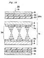
- Fig. 13 is an exploded cross sectional view of a liquid crystal display device 31 of a second preferred embodiment according to the present invention.
- the components similar to that shown in Fig. 7 are indicated by the same numerical reference as that shown in Fig. 7.
- the liquid crystal display device 31 is made as follows.
- a display cell layer 1b for displaying an image thereon is made in the manner similar to that of the first cell layer 1 of the liquid crystal display device 18 of the first preferred embodiment shown in Fig. 7, except for a liquid crystal layer 32 which is contained between a pair of optically transparent substrates 3 and 4.
- a liquid crystal material of the liquid crystal layer 32 there is used a mixed liquid crystal of a nematic liquid crystal material having positive dielectric anisotropy such as liquid crystal of phenylcyclohexane (PCH) group, to which 0.1 wt% of a chiral dopant S-811® made by Merk & Co., Inc. is added in order to regulate the twist direction thereof.
- the birefringence ⁇ n3 of the liquid crystal layer 32 is set at 0.096, and the thickness d3 thereof is set at 6.0 ⁇ ms.
- a pair of phase difference cancellation films 28 and 29 are formed on respective outer surfaces of the optically transparent substrates 3 and 4, and a pair of polarizer 15 and 16 are formed on respective outer surfaces of the phase difference cancellation films 28 and 29.
- a film 30 for compensating a change in the retardation (referred to as a retardation compensation film hereinafter) according to the present invention is further arranged between the phase difference cancellation film 29 and the polarizer 16.
- Each of the phase difference cancellation films 28 and 29 is a uniaxially drawn polycarbonate film having predetermined optical axis, and the retardation thereof is 200 nms for the light transmitting in a direction of the normal perpendicular to respective surfaces of the phase difference cancellation films 28 and 29.
- the retardation compensation film 30 is made of polystyrene, and the retardation (n a -n b ) ⁇ d5 thereof is 30 nms for the light transmitting in a direction of the normal perpendicular to the surface of the retardation compensation film 30, wherein n a and n b (n a > n b ) are two kinds of principal refractive indices in a direction parallel to the surface of the retardation compensation film 30, and d5 is the thickness thereof.
- the retardation (n c -n b ) ⁇ d5 is 70 nms for the light transmitting in the direction parallel to the surface of the retardation compensation film 30, wherein n c is another principal refractive index in the direction of the normal perpendicular to the surfaces of the retardation compensation film 30, which is a maximum one of the principal refractive indices.
- Fig. 14 shows a relationship among orientation angles of the liquid crystal of the liquid crystal layer 32, respective optical axes of the phase difference cancellation films 28 and 29, the optical axis of the retardation compensation film 30, and respective polarization axes of the polarizers 15 and 16, when seeing in the direction perpendicular to respective surfaces of the optically transparent substrates 3 and 4 of the liquid crystal display device 31 shown in Fig. 13.
- respective directions are represented by using the positions of respective hours on displayed on a clock.
- the up and down directions in Fig. 13 correspond to directions of 6 o'clock and 12 o'clock shown in Fig. 14, and the left and right directions correspond to directions of 3 o'clock and 9 o'clock shown in Fig. 14.
- Figs. 17 and 20 respective orientation angles of the components are also represented in the manner similar to that shown in Fig. 14.
- the principal axes of the liquid crystal molecules of the liquid crystal layer 32 which are arranged on the side of the optically transparent substrate 3 are parallel to a direction as indicated by an arrow a3 which is rotated by an angle of 45° from the direction of 6 o'clock toward the direction of 9 o'clock, and the principal axes thereof which are arranged on the side of the optically transparent substrate 4 are parallel to a direction as indicated by an arrow a4 which is further rotated in the clockwise direction by right angle from the direction as indicated by the arrow a3.
- Respective directions of the maximum one of the principal refractive indices or the optical axis of the phase difference cancellation films 28 and 29 coincide with the directions as indicated by the arrows a4 and a3.
- the polarization direction of the polarizer 15 is oriented in a direction as indicated by an arrow a15, which is rotated at an angle of 25° from the direction of 6 o'clock toward the direction of 3 o'clock
- the polarization direction of the polarizer 16 is oriented in a direction as indicated by an arrow a16, which is rotated by an angle of 65° from the direction of 6 o'clock toward the direction of 3 o'clock.
- the drawing direction or the direction of the aforementioned principal refractive index n a of the retardation compensation film 30 is oriented in the directions of 3 o'clock and 9 o'clock.
- the relationship among these orientation directions is suitably determined so as to enlarge the range of the viewing angle ⁇ to improve the contrast ratio upon displaying an image on the liquid crystal display device. In the cases of Figs. 17 and 20 as described later, this relationship is determined, similarly.
- Figs. 15a and 15b are graphs showing contrast ratio characteristics on the viewing angle of the liquid crystal display device 31.
- a characteristic curve l10 shows a contrast ratio characteristic on the viewing angle when seeing from a plane including the aforementioned directions of 6 o'clock and 12 o'clock perpendicular to respective surfaces of the optically transparent substrates 3 and 4 of the liquid crystal display device 31, and a characteristic curve l11 shows the same characteristic of the conventional liquid crystal display device 17 shown in Fig. 1.
- Fig. 15a characteristic curve l10 shows a contrast ratio characteristic on the viewing angle when seeing from a plane including the aforementioned directions of 6 o'clock and 12 o'clock perpendicular to respective surfaces of the optically transparent substrates 3 and 4 of the liquid crystal display device 31
- a characteristic curve l11 shows the same characteristic of the conventional liquid crystal display device 17 shown in Fig. 1.
- a characteristic curve l12 shows the same characteristic of the liquid crystal display device 31 when seeing from a plane including the aforementioned directions of 3 o'clock and 9 o'clock
- a characteristic curve l13 shows the same characteristic of the conventional liquid crystal display device 17.
- Figs. 15a and 15b it is understood that, in the case of a contrast ratio equal to or larger than five, the range of the viewing angle in the directions 6 o'clock and 12 o'clock is enlarged by an angle equal to or larger than 26°, and the range thereof in the directions of 3 o'clock and 9 o'clock is enlarged by an angle equal to or larger than 7°.
- the TN type liquid crystal display device according to the present invention is described above, however, the present invention is not limited to this.
- the present invention is applied to an STN type liquid crystal display device having a twist angle of the liquid crystal which is equal to or larger than 90°.
- Fig. 16 is an exploded cross sectional view showing a liquid crystal display device 33 of a third preferred embodiment according to the present invention.
- the components similar to that shown in Figs. 7 and 13 are indicated by the same numerical references as that shown in Figs. 7 and 13.
- the liquid crystal display device 33 is made as follows.
- a display cell layer 1c for displaying an image is made in the manner similar to that of the second preferred embodiment shown in Fig. 13, except for a pair of orientation membranes 7a and 8a and a liquid crystal layer 34. Namely, respective inner surfaces of the orientation membranes 7a and 8a are previously treated by rubbing with cloth so that the liquid crystal of the liquid crystal layer 34 is twisted at an angle of 240°.
- a pair of phase difference cancellation films 28 and 29 are formed on respective outer surfaces of the optically transparent substrates 3 and 4, and a pair of polarizers 15 and 16 are formed on respective outer surfaces of the phase difference cancellation films 28 and 29.
- a retardation compensation film 35 according to the present invention is further arranged between the phase difference cancellation film 29 and the polarizer 16.
- liquid crystal material of the liquid crystal layer 34 there is used a mixed liquid crystal of a nematic liquid crystal material having a positive dielectric anisotropy such as liquid crystal of phenylcyclohexane (PCH) group and pyrimidine group, to which 0.76 wt% of a chiral dopant S-811® made by Merk & Co., Inc. is added in order to regulate the twist direction thereof.
- the birefringence ⁇ n4 of the liquid crystal layer 34 is set at 0.123, and the thickness d4 thereof is set at 7.5 ⁇ ms.
- Each of the phase difference cancellation films 28 and 29 is a uniaxially drawn polycarbonate film having a predetermined optical axis, and the retardation thereof is 400 nms for the light transmitting in a direction of the normal perpendicular to respective surfaces of the phase difference cancellation films 28 and 29.
- the retardation compensation film 35 is made of polystyrene, and the retardation (n a -n b ) ⁇ d6 thereof is 30 nms for the light transmitting in a direction of the normal perpendicular to the surface of the retardation compensation film 35, wherein d6 is the thickness thereof.
- the retardation (n c -n b ) ⁇ d6 is 70 nms for the light transmitting in the direction parallel to the surface of the retardation compensation film 35.
- Fig. 17 shows a relationship among orientation angles of the liquid crystal of the liquid crystal layer 34, respective optical axes of the phase difference cancellation films 28 and 29, the optical axis of the retardation compensation film 35, and respective polarization axes of the polarizers 15 and 16, when seeing in the direction perpendicular to respective surfaces of the optically transparent substrates 3 and 4 of the liquid crystal display device 33 shown in Fig. 16.
- the principal axes of the liquid crystal molecules of the liquid crystal layer 34 which are arranged on the side of the optically transparent substrate 3 are parallel to a direction as indicated by an arrow a3 which is rotated at an angle of 60° from the direction of 6 o'clock toward the direction of 3 o'clock, and the principal axes thereof which are arranged on the side of the optically transparent substrate 4 are parallel to a direction as indicated by the arrow a4 which is rotated by an angle of 240° in the counterclockwise direction from the direction as indicated by the arrow a3.
- the direction of the maximum one of the principal refractive indices or the optical axis of the phase difference cancellation film 28 is oriented in a direction as indicated by an arrow a28 which is rotated by an angle of 20° from the direction of 6 o'clock toward the direction of 9 o'clock
- the direction of the maximum one of the principal refractive indices or the optical axis of the phase difference cancellation film 29 is oriented in a direction as indicated by an arrow a29 which is rotated by an angle of 20° from the direction of 6 o'clock to the direction of 3 o'clock.
- the polarization direction of the polarizer 15 is oriented in a direction as indicated by an arrow a15 which is rotated by an angle of 10° from the direction of 6 o'clock toward the direction of 3 o'clock
- the polarization direction of the polarizer 16 is oriented in a direction as indicated by an arrow a16, which is rotated by an angle of 80° from the direction of 6 o'clock toward the direction of 3 o'clock.
- the drawing direction or the direction of the aforementioned principal refractive index n a of the retardation compensation film 35 is oriented in a direction as indicated by an arrow a35 which is rotated at an angle of 65° from the direction of 6 o'clock toward the direction of 3 o'clock.
- Figs. 18a and 18b are graphs showing contrast ratio characteristics on the viewing angle of the liquid crystal display device 33.
- a characteristic curve l15 shows a contrast ratio characteristic on the viewing angle when seeing from a plane including the aforementioned directions of 6 o'clock and 12 o'clock of the liquid crystal display device 33
- a characteristic curve l14 shows the same characteristic of conventional liquid crystal display device 26 shown in Fig. 6.
- a characteristic curve l17 shows the same characteristic of the liquid crystal display device 33 when seeing from a plane including the aforementioned directions of 3 o'clock and 9 o'clock
- a characteristic curve l16 shows the same characteristic of the conventional liquid crystal display device 26.
- Fig. 19 is an exploded cross sectional view of a liquid crystal display device 36 of a fourth preferred embodiment according to the present invention.
- the components similar to that shown in Figs. 7, 13 and 16 are indicated by the same numerical references as that shown in Figs. 7, 13 and 16.
- the liquid crystal display device 36 is made as follows.
- a display cell layer 1c for displaying an image is made in the manner similar to that of the third preferred embodiment.
- a retardation compensation film 38 according to the present invention is further arranged between the phase difference film 29 and the polarizer 16.
- Each of the phase difference cancellation films 39, 40 and 29 is a uniaxially drawn polycarbonate film having a predetermined optical axis, and the retardations thereof are 200 nms, 200 nms and 400 nms, respectively, for the light transmitting in a direction of the normal perpendicular to respective surfaces of the phase difference cancellation films 39, 40 and 29.
- the retardation compensation film 38 is made of polystyrene.
- the retardation (n a -n b ) ⁇ d4 of the retardation compensation film 38 is 30 nms for the light transmitting in a direction of the normal perpendicular to the surface of the retardation compensation film 38, and the retardation (n c -n b ) ⁇ d4 thereof is 70 nms for the light transmitting in a direction parallel to the surface thereof.
- Fig. 20 shows a relationship among orientation angles of the liquid crystal of the liquid crystal layer 34, respective optical axes of the phase difference cancellation films 39, 40 and 29, the optical axis of the retardation compensation film 38, and respective polarization axes of the polarizers 15 and 16, when seeing in the direction perpendicular to respective surfaces of the optically transparent substrates 3 and 4 of the liquid crystal display device 36 shown in Fig. 19.
- the principal axes of the liquid crystal molecules of the liquid crystal layer 34 which are arranged on the side of the optically transparent substrate 4 are parallel to a direction as indicated by an arrow a4 which is rotated by an angle of 60° from the direction of 6 o'clock toward the direction of 9 o'clock, and the principal axes thereof which are arranged on the side of the optically transparent substrate 3 are parallel to a direction as indicated by an arrow a3 which is rotated at an angle of 240° from the direction as indicated by the arrow a4 in the counterclockwise direction.
- the direction of the maximum one of the principal refractive indices or the optical axis of the phase difference cancellation film 39 is oriented in a direction as indicated by an arrow a39 which is rotated by an angle of 55° from the direction of 6 o'clock toward the direction of 9 o'clock
- the direction of the maximum one of the principal refractive indices or the optical axis of the phase difference cancellation film 40 is oriented in a direction as indicated by an arrow a40 which is rotated by an angle of 25° from the direction of 6 o'clock to the direction of 9 o'clock. Therefore, the direction of the refractive indices of the phase difference films 39 and 40 cross each other at an angle of 30°.
- the direction of the maximum one of the principal refractive indices of the phase difference film 29 is oriented in a direction as indicated by an arrow a29 which is rotated by an angle of 25° from the direction of 6 o'clock toward the direction of 3 o'clock.
- the polarization direction of the polarizer 15 is oriented in a direction as indicated by an arrow a15, which is rotated by an angle of 40° from the direction of 6 o'clock toward the direction of 9 o'clock
- the polarization direction of the polarizer 16 is oriented in a direction as indicated by an arrow a16, which is rotated at an angle of 75° from the direction of 6 o'clock toward the direction of 3 o'clock.
- drawing direction or the direction of the aforementioned principal refractive index of n a of the retardation compensation film 38 is oriented in a direction as indicated by an arrow a38 which is parallel to the polarization direction a16 of the polarizer 16.
- Figs. 21a and 21b are graphs showing contrast ratio characteristics on the viewing angle of the liquid crystal display device 36.
- a characteristic curve l19 shows a contrast ratio characteristic on the viewing angle when seeing from a plane including the aforementioned directions of 6 o'clock and 12 o'clock perpendicular to respective surfaces of the optically transparent substrates 3 and 4 of the liquid crystal display device 36
- a characteristic curve l18 shows the same characteristic of the conventional liquid crystal display device 26 shown in Fig. 6.
- Fig. 21a shows a contrast ratio characteristic on the viewing angle when seeing from a plane including the aforementioned directions of 6 o'clock and 12 o'clock perpendicular to respective surfaces of the optically transparent substrates 3 and 4 of the liquid crystal display device 36
- a characteristic curve l18 shows the same characteristic of the conventional liquid crystal display device 26 shown in Fig. 6.
- a characteristic curve l21 shows the same characteristic of the liquid crystal display device 36 when seeing from a plane including the aforementioned directions of 3 o'clock and 9 o'clock
- a characteristic curve l20 shows the same characteristic of the conventional liquid crystal display device 26.
- Figs. 21a and 21b it is understood that the viewing angle characteristic in the directions of 6 o'clock and 12 o'clock is improved as compared with that of the liquid crystal display device 33 of the third preferred embodiment, and further, in the case of a contrast ratio of five, the range of the viewing angle in the directions thereof is enlarged by an angle equal to or larger than 10°, as compared with that of the conventional liquid crystal display device 26.
- the phase difference cancellation film 28a is composed of laminated plural phase difference cancellation films, the contrast ratio is heightened, resulting in a distinct monochromatic display such as a white and black display.
- the retardation compensation film having the optical birefringence wherein the direction of the maximum one of the principal refractive indices becomes substantially parallel to the direction of the normal perpendicular to respective surfaces of the optically transparent substrates of the display cell layer for displaying an image thereon, can be made of a film obtained by shaping a polymeric liquid crystal material or an ionic liquid crystal material into a film configuration, or can be made of a polymer film wherein the bias of the distribution density of electrons thereof is produced in the direction of the thickness thereof such as polystyrene.
- the retardation for the light transmitting in the direction perpendicular to respective surfaces of the substrates of the liquid crystal display cell layer or in the direction of thickness of the retardation compensation film increases as the viewing angle increases.
- the sum of a change in the retardation caused when light passes through the first cell layer 1 or the display cell layer and a change in the retardation of the second cell layer 2 or the retardation compensation film is preferably set so as not to change depending on the viewing angle.
- the peak value T ⁇ peak of the light transmittance can be canceled by arranging the second cell layer 2 for compensating a change in the retardation, the retardation compensation films 30, 35 or 38, or the like, resulting in improved viewing angle characteristics.
- the present invention can be suitably applied to an active drive type liquid crystal display device or the like for driving a liquid crystal display cell by using active devices such as Thin Film Transistors, Metal Insulator Metal devices, diodes.
Landscapes
- Physics & Mathematics (AREA)
- Nonlinear Science (AREA)
- Chemical & Material Sciences (AREA)
- Crystallography & Structural Chemistry (AREA)
- General Physics & Mathematics (AREA)
- Optics & Photonics (AREA)
- Mathematical Physics (AREA)
- Liquid Crystal (AREA)
Applications Claiming Priority (4)
| Application Number | Priority Date | Filing Date | Title |
|---|---|---|---|
| JP310893/88 | 1988-12-07 | ||
| JP31089388 | 1988-12-07 | ||
| JP267235/89 | 1989-10-13 | ||
| JP1267235A JP2675158B2 (ja) | 1988-12-07 | 1989-10-13 | 液晶表示装置 |
Publications (3)
| Publication Number | Publication Date |
|---|---|
| EP0372973A2 true EP0372973A2 (fr) | 1990-06-13 |
| EP0372973A3 EP0372973A3 (fr) | 1991-03-06 |
| EP0372973B1 EP0372973B1 (fr) | 1995-08-09 |
Family
ID=26547775
Family Applications (1)
| Application Number | Title | Priority Date | Filing Date |
|---|---|---|---|
| EP89312788A Expired - Lifetime EP0372973B1 (fr) | 1988-12-07 | 1989-12-07 | Dispositif d'affichage à cristal liquide avec des caractéristiques d'angle de vision modifiées |
Country Status (5)
| Country | Link |
|---|---|
| US (1) | US5124824A (fr) |
| EP (1) | EP0372973B1 (fr) |
| JP (1) | JP2675158B2 (fr) |
| KR (1) | KR940009075B1 (fr) |
| DE (1) | DE68923768T2 (fr) |
Cited By (8)
| Publication number | Priority date | Publication date | Assignee | Title |
|---|---|---|---|---|
| EP0412844A1 (fr) * | 1989-08-11 | 1991-02-13 | SHARP Corporation | Affichage à cristal liquide |
| EP0424951A1 (fr) * | 1989-10-27 | 1991-05-02 | Fuji Photo Film Co., Ltd. | Dispositif d'affichage à cristal liquide |
| EP0465133A2 (fr) * | 1990-06-27 | 1992-01-08 | Nippon Oil Company, Limited | Procédé de fabrication d'un compensateur pour afficheur à cristaux liquides |
| EP0478383A2 (fr) * | 1990-09-28 | 1992-04-01 | Sharp Kabushiki Kaisha | Dispositif d'affichage à cristal liquide |
| EP0479551A2 (fr) * | 1990-10-01 | 1992-04-08 | Sharp Kabushiki Kaisha | Dispositif d'affichage à cristal liquide |
| EP0487359A2 (fr) * | 1990-11-22 | 1992-05-27 | Sharp Kabushiki Kaisha | Afficheur à cristal liquide |
| EP0529813A2 (fr) * | 1991-07-29 | 1993-03-03 | Nippon Oil Co., Ltd. | Compensateur pour un afficheur à cristal liquide |
| EP0622656A1 (fr) * | 1993-04-30 | 1994-11-02 | Rockwell International Corporation | Compensateur optique pour dispositif d'affichage à cristaux liquides |
Families Citing this family (47)
| Publication number | Priority date | Publication date | Assignee | Title |
|---|---|---|---|---|
| US5189538A (en) * | 1988-11-04 | 1993-02-23 | Fuji Photo Film Co., Ltd. | Liquid crystal display having positive and negative birefringent compensator films |
| KR970009490B1 (ko) * | 1989-03-28 | 1997-06-13 | 아사히가라스 가부시끼가이샤 | 액정 디스플레이 장치 |
| US5175638A (en) * | 1989-09-12 | 1992-12-29 | Ricoh Company, Ltd. | ECB type liquid crystal display device having birefringent layer with equal refractive indexes in the thickness and plane directions |
| US5380459A (en) * | 1990-04-20 | 1995-01-10 | Ricoh Company, Ltd. | Liquid crystal display device with improved viewing angle dependence of color |
| US5184236A (en) * | 1990-08-10 | 1993-02-02 | Casio Computer Co., Ltd. | Twisted nematic liquid crystal display device with retardation plates having phase axis direction within 15° of alignment direction |
| US5237438A (en) * | 1991-05-02 | 1993-08-17 | Casio Computer Co., Ltd. | Liquid crystal display device |
| DE69228843T2 (de) * | 1991-05-27 | 1999-08-26 | Dainippon Ink And Chemicals | Flüssigkristallvorrichtung |
| JP2856942B2 (ja) * | 1991-05-28 | 1999-02-10 | 株式会社東芝 | 液晶表示素子および光学異方素子 |
| US5196953A (en) * | 1991-11-01 | 1993-03-23 | Rockwell International Corporation | Compensator for liquid crystal display, having two types of layers with different refractive indices alternating |
| JP2796210B2 (ja) * | 1992-01-30 | 1998-09-10 | シャープ株式会社 | 液晶表示装置 |
| TW229279B (fr) * | 1992-06-18 | 1994-09-01 | Casio Computer Co Ltd | |
| US5583678A (en) * | 1993-03-12 | 1996-12-10 | Casio Computer Co., Ltd. | Color liquid crystal display apparatus |
| CA2119484A1 (fr) * | 1993-03-25 | 1994-09-26 | Toshihiro Ohnishi | Materiau optiquement anisotrope, sa methode de fabrication et plaque de retardement et afficheur a cristaux liquides utilisant ce materiau |
| JP3401049B2 (ja) * | 1993-05-26 | 2003-04-28 | コーニンクレッカ フィリップス エレクトロニクス エヌ ヴィ | 階調液晶表示パネル |
| US5550661A (en) * | 1993-11-15 | 1996-08-27 | Alliedsignal Inc. | Optical phase retardation film |
| US5499126A (en) | 1993-12-02 | 1996-03-12 | Ois Optical Imaging Systems, Inc. | Liquid crystal display with patterned retardation films |
| US5570214A (en) * | 1993-12-15 | 1996-10-29 | Ois Optical Imaging Systems, Inc. | Normally white twisted nematic LCD with retardation films on opposite sides of liquid crystal material for improved viewing zone |
| US5594568A (en) * | 1993-12-15 | 1997-01-14 | Ois Optical Imaging Systems, Inc. | LCD with a pair of retardation films on one side of normally white liquid crystal layer |
| US5576861A (en) | 1993-12-15 | 1996-11-19 | Ois Optical Imaging Systems, Inc. | Liquid crystal display having a retarder with 100-200nm retardation and having high contrast viewing zone centered in positive or negative vertical region |
| US5907378A (en) * | 1993-12-15 | 1999-05-25 | Ois Optical Imaging Systems, Inc. | Normally white twisted nematic liquid crystal display including retardation films for improving viewing characteristics |
| US5657140A (en) * | 1993-12-15 | 1997-08-12 | Ois Optical Imaging Systems, Inc. | Normally white twisted nematic LCD with positive and negative retarders |
| US5724112A (en) * | 1994-03-28 | 1998-03-03 | Casio Computer Co., Ltd. | Color liquid crystal apparatus |
| US5986734A (en) * | 1994-04-04 | 1999-11-16 | Rockwell International Corporation | Organic polymer O-plate compensator for improved gray scale performance in twisted nematic liquid crystal displays |
| US5504603A (en) * | 1994-04-04 | 1996-04-02 | Rockwell International Corporation | Optical compensator for improved gray scale performance in liquid crystal display |
| US5619352A (en) * | 1994-04-04 | 1997-04-08 | Rockwell International Corporation | LCD splay/twist compensator having varying tilt and /or azimuthal angles for improved gray scale performance |
| US5680184A (en) * | 1994-04-12 | 1997-10-21 | Casio Computer Co., Ltd. | Color liquid crystal display device |
| US5638200A (en) * | 1995-02-03 | 1997-06-10 | Ois Optical Imaging Systems, Inc. | Liquid crystal display with tilted retardation film |
| US5610743A (en) * | 1995-10-30 | 1997-03-11 | United Microelectronics Corporation | Liquid crystal display including concentric shapes and radial spokes which has an improved viewing angle |
| US5870159A (en) * | 1995-10-30 | 1999-02-09 | Kaj | Switchable achromatic polarization rotator |
| JPH09292611A (ja) | 1996-04-30 | 1997-11-11 | Nec Corp | 液晶表示装置 |
| JP3032424U (ja) * | 1996-06-14 | 1996-12-24 | セイコー電子工業株式会社 | 液晶表示装置およびその液晶表示装置を備えた携帯機器 |
| GB2314640A (en) * | 1996-06-26 | 1998-01-07 | Sharp Kk | Liquid crystal devices |
| GB2314641A (en) * | 1996-06-26 | 1998-01-07 | Sharp Kk | Liquid crystal devices |
| JP3452755B2 (ja) * | 1997-04-07 | 2003-09-29 | シャープ株式会社 | 液晶表示装置 |
| US5948487A (en) * | 1997-09-05 | 1999-09-07 | 3M Innovative Properties Company | Anisotropic retardation layers for display devices |
| JP2000310774A (ja) * | 1999-04-28 | 2000-11-07 | Asahi Glass Co Ltd | カラー液晶表示装置 |
| JP2001042127A (ja) * | 1999-08-04 | 2001-02-16 | Nitto Denko Corp | 複合位相差板、光学補償偏光板及び液晶表示装置 |
| US6538714B1 (en) | 1999-10-25 | 2003-03-25 | 3M Innovative Properties Company | Dual color guest-host polarizers and devices containing guest-host polarizers |
| US6574044B1 (en) * | 1999-10-25 | 2003-06-03 | 3M Innovative Properties Company | Polarizer constructions and display devices exhibiting unique color effects |
| CN1335943B (zh) * | 1999-11-02 | 2010-05-26 | 精工爱普生株式会社 | 反射型及半透射反射型液晶装置以及电子设备 |
| US7498739B1 (en) * | 2004-09-30 | 2009-03-03 | Rockwell Collins, Inc. | Polarized light source using an organic liquid crystal |
| US20070248771A1 (en) * | 2006-04-21 | 2007-10-25 | Nitto Denko Corporation | Acenaphtho[1,2-b]quinoxaline sulfo-and carboxy-derivative, lyotropic liquid crystal system, optically anisotropic film and method thereof and laminated optical film |
| US8836879B2 (en) | 2010-06-10 | 2014-09-16 | Apple Inc. | Displays with minimized curtain mura |
| CN102411232B (zh) * | 2010-09-17 | 2015-01-21 | 上海天马微电子有限公司 | 液晶显示装置及其制造方法 |
| KR20150042607A (ko) * | 2013-10-11 | 2015-04-21 | 삼성디스플레이 주식회사 | 액정 표시 장치 |
| KR20170088596A (ko) * | 2016-01-25 | 2017-08-02 | 삼성전자주식회사 | 액정 캡슐 층을 구비한 디스플레이 장치 및 디스플레이 패널 |
| TWI797010B (zh) * | 2022-04-28 | 2023-03-21 | 大陸商業成科技(成都)有限公司 | 曲面光學結構及其製造方法 |
Citations (5)
| Publication number | Priority date | Publication date | Assignee | Title |
|---|---|---|---|---|
| JPS63271429A (ja) * | 1987-04-30 | 1988-11-09 | Seiko Epson Corp | 液晶表示装置 |
| JPS63271415A (ja) * | 1987-04-30 | 1988-11-09 | Seiko Epson Corp | 液晶表示装置 |
| EP0315484A2 (fr) * | 1987-11-04 | 1989-05-10 | Sharp Kabushiki Kaisha | Dispositif d'affichage à cristal liquide |
| JPH01219720A (ja) * | 1988-02-26 | 1989-09-01 | Seiko Epson Corp | 液晶電気光学素子 |
| JPH0247269A (ja) * | 1988-08-04 | 1990-02-16 | Kawasaki Steel Corp | 耐型かじり性にすぐれた冷延鋼板およびその製造方法 |
Family Cites Families (22)
| Publication number | Priority date | Publication date | Assignee | Title |
|---|---|---|---|---|
| GB1462978A (en) * | 1974-04-17 | 1977-01-26 | Rank Organisation Ltd | Optical apparatus |
| US4385806A (en) * | 1978-06-08 | 1983-05-31 | Fergason James L | Liquid crystal display with improved angle of view and response times |
| US4443065A (en) * | 1980-12-09 | 1984-04-17 | Sharp Kabushiki Kaisha | Interference color compensation double layered twisted nematic display |
| JPS58143305A (ja) * | 1982-02-22 | 1983-08-25 | Hitachi Ltd | 表示パネル |
| JPS5977401A (ja) * | 1982-09-22 | 1984-05-02 | Nitto Electric Ind Co Ltd | 偏光板 |
| FR2564605B1 (fr) * | 1984-05-18 | 1987-12-24 | Commissariat Energie Atomique | Cellule a cristal liquide susceptible de presenter une structure homeotrope, a birefringence compensee pour cette structure |
| GB2171549B (en) * | 1985-02-15 | 1988-05-18 | Citizen Watch Co Ltd | Liquid crystal display device |
| FR2595157B1 (fr) * | 1986-02-28 | 1988-04-29 | Commissariat Energie Atomique | Cellule a double couche de cristal liquide, utilisant l'effet de birefringence controlee electriquement et procede de fabrication d'un milieu uniaxe d'anisotropie optique negative utilisable dans cette cellule |
| FR2595156B1 (fr) * | 1986-02-28 | 1988-04-29 | Commissariat Energie Atomique | Cellule a cristal liquide utilisant l'effet de birefringence controlee electriquement et procedes de fabrication de la cellule et d'un milieu uniaxe d'anisotropie optique negative, utilisable dans celle-ci |
| EP0246842B1 (fr) * | 1986-05-19 | 1998-09-23 | Seiko Epson Corporation | Dispositif d'affichage à cristal liquide |
| US4767190A (en) * | 1986-12-04 | 1988-08-30 | Xerox Corporation | Transient state liquid crystal image bar with contrast enhancement |
| FR2613566B1 (fr) * | 1987-04-06 | 1989-06-09 | Commissariat Energie Atomique | Ecran a matrice active pour affichage en couleur d'images de television, systeme de commande et procede de fabrication dudit ecran |
| US4906073A (en) * | 1987-07-29 | 1990-03-06 | Hitachi, Ltd. | Liquid crystal display device using nematic liquid crystal having twisted helical structure and a phase correction plate |
| US4984873A (en) * | 1987-08-31 | 1991-01-15 | Ricoh Company, Ltd. | Liquid crystal display device |
| JPH01243019A (ja) * | 1988-03-24 | 1989-09-27 | Sharp Corp | カラー液晶表示装置 |
| JPH0215238A (ja) * | 1988-07-04 | 1990-01-18 | Stanley Electric Co Ltd | 異方性補償ホメオトロピック液晶表示装置 |
| JP2718078B2 (ja) * | 1988-08-09 | 1998-02-25 | セイコーエプソン株式会社 | 液晶電気光学素子 |
| US5056896A (en) * | 1988-08-29 | 1991-10-15 | Ricoh Company, Ltd. | Liquid crystal display device with dielectric anisotropy |
| JPH0273327A (ja) * | 1988-09-09 | 1990-03-13 | Ricoh Co Ltd | 液晶表示素子 |
| JP3071204B2 (ja) * | 1989-02-10 | 2000-07-31 | 株式会社リコー | 液晶表示素子 |
| JP2915430B2 (ja) * | 1989-04-27 | 1999-07-05 | 旭硝子株式会社 | 液晶表示素子 |
| JP2775827B2 (ja) * | 1989-04-06 | 1998-07-16 | 旭硝子株式会社 | 液晶表示素子 |
-
1989
- 1989-10-13 JP JP1267235A patent/JP2675158B2/ja not_active Expired - Fee Related
- 1989-12-05 US US07/446,305 patent/US5124824A/en not_active Expired - Lifetime
- 1989-12-06 KR KR1019890018047A patent/KR940009075B1/ko not_active IP Right Cessation
- 1989-12-07 EP EP89312788A patent/EP0372973B1/fr not_active Expired - Lifetime
- 1989-12-07 DE DE68923768T patent/DE68923768T2/de not_active Expired - Fee Related
Patent Citations (5)
| Publication number | Priority date | Publication date | Assignee | Title |
|---|---|---|---|---|
| JPS63271429A (ja) * | 1987-04-30 | 1988-11-09 | Seiko Epson Corp | 液晶表示装置 |
| JPS63271415A (ja) * | 1987-04-30 | 1988-11-09 | Seiko Epson Corp | 液晶表示装置 |
| EP0315484A2 (fr) * | 1987-11-04 | 1989-05-10 | Sharp Kabushiki Kaisha | Dispositif d'affichage à cristal liquide |
| JPH01219720A (ja) * | 1988-02-26 | 1989-09-01 | Seiko Epson Corp | 液晶電気光学素子 |
| JPH0247269A (ja) * | 1988-08-04 | 1990-02-16 | Kawasaki Steel Corp | 耐型かじり性にすぐれた冷延鋼板およびその製造方法 |
Non-Patent Citations (3)
| Title |
|---|
| PATENT ABSTRACTS OF JAPAN, vol. 13, no. 533 (P-967)[3381], 28th November 1989; & JP-A-1 219 720 (SEIKO EPSON CORP.) 01-09-1989 * |
| PATENT ABSTRACTS OF JAPAN, vol. 13, no. 89 (P-836)[3437], 2nd March 1989; & JP-A-63 271 415 (SEIKO EPSON CORP.) 09-11-1988 * |
| PATENT ABSTRACTS OF JAPAN, vol. 14, no. 214 (P-1044)[4157], 7th May 1990; & JP-A-2 047 269 (SEIKO EPSON CORP.) 16-02-1990 * |
Cited By (19)
| Publication number | Priority date | Publication date | Assignee | Title |
|---|---|---|---|---|
| EP0412844A1 (fr) * | 1989-08-11 | 1991-02-13 | SHARP Corporation | Affichage à cristal liquide |
| US5126866A (en) * | 1989-08-11 | 1992-06-30 | Sharp Kabushiki Kaisha | Liquid crystal display with a plurality of phase difference plates the slow axes of which form an angle of 20 to 40 degrees |
| EP0424951A1 (fr) * | 1989-10-27 | 1991-05-02 | Fuji Photo Film Co., Ltd. | Dispositif d'affichage à cristal liquide |
| US5138474A (en) * | 1989-10-27 | 1992-08-11 | Fuji Photo Film Co., Ltd. | Liquid crystal display with compensator having two films with positive and negative intrinsic birefringence, respectively |
| EP0465133A2 (fr) * | 1990-06-27 | 1992-01-08 | Nippon Oil Company, Limited | Procédé de fabrication d'un compensateur pour afficheur à cristaux liquides |
| EP0465133A3 (en) * | 1990-06-27 | 1992-06-03 | Nippon Oil Co., Ltd. | Method for producing compensator for liquid crystal display |
| EP0478383A3 (en) * | 1990-09-28 | 1992-11-25 | Sharp Kabushiki Kaisha | Liquid crystal display apparatus |
| EP0478383A2 (fr) * | 1990-09-28 | 1992-04-01 | Sharp Kabushiki Kaisha | Dispositif d'affichage à cristal liquide |
| US5235450A (en) * | 1990-09-28 | 1993-08-10 | Sharp Kabushiki Kaisha | Liquid crystal display apparatus with positive and negative phase plates with specific positions of slow axes |
| EP0479551A2 (fr) * | 1990-10-01 | 1992-04-08 | Sharp Kabushiki Kaisha | Dispositif d'affichage à cristal liquide |
| EP0479551A3 (en) * | 1990-10-01 | 1992-11-25 | Sharp Kabushiki Kaisha | Liquid crystal display device |
| US5291323A (en) * | 1990-10-01 | 1994-03-01 | Sharp Kabushiki Kaisha | Liquid crystal display device with positive and negative compensating films each with its optical axis parallel to the surface |
| EP0487359A3 (en) * | 1990-11-22 | 1992-11-25 | Sharp Kabushiki Kaisha | A liquid crystal display |
| EP0487359A2 (fr) * | 1990-11-22 | 1992-05-27 | Sharp Kabushiki Kaisha | Afficheur à cristal liquide |
| US5249071A (en) * | 1990-11-22 | 1993-09-28 | Sharp Kabushiki Kaisha | Liquid crystal display having positive and negative uniaxially oriented polymer films |
| EP0529813A2 (fr) * | 1991-07-29 | 1993-03-03 | Nippon Oil Co., Ltd. | Compensateur pour un afficheur à cristal liquide |
| EP0529813A3 (en) * | 1991-07-29 | 1993-11-03 | Nippon Oil Co Ltd | Compensator for a liquid crystal display |
| EP0622656A1 (fr) * | 1993-04-30 | 1994-11-02 | Rockwell International Corporation | Compensateur optique pour dispositif d'affichage à cristaux liquides |
| US5986733A (en) * | 1993-04-30 | 1999-11-16 | Rockwell International Corporation | Negative optical compensator tilted in respect to liquid crystal cell for liquid crystal display |
Also Published As
| Publication number | Publication date |
|---|---|
| JPH02256021A (ja) | 1990-10-16 |
| EP0372973B1 (fr) | 1995-08-09 |
| KR940009075B1 (ko) | 1994-09-29 |
| JP2675158B2 (ja) | 1997-11-12 |
| KR910012768A (ko) | 1991-08-08 |
| US5124824A (en) | 1992-06-23 |
| DE68923768D1 (de) | 1995-09-14 |
| DE68923768T2 (de) | 1996-02-22 |
| EP0372973A3 (fr) | 1991-03-06 |
Similar Documents
| Publication | Publication Date | Title |
|---|---|---|
| EP0372973B1 (fr) | Dispositif d'affichage à cristal liquide avec des caractéristiques d'angle de vision modifiées | |
| US5016988A (en) | Liquid crystal display device with a birefringent compensator | |
| EP0821261B1 (fr) | Dispositif d'affichage à cristaux liquides du type réflectif | |
| EP0539847B1 (fr) | Compensateur pour afficheur à cristal liquide | |
| EP0622656B1 (fr) | Compensateur optique pour dispositif d'affichage à cristaux liquides | |
| US5126868A (en) | Color compensated double layered liquid crystal display device | |
| US5541753A (en) | Liquid crystal display and device having a total retardance of (M+1) λ/2 and (Mλ/2) at first and second operating voltages | |
| EP0351200A2 (fr) | Dispositif d'affichage à cristaux liquides | |
| US4904058A (en) | Liquid crystal display panel | |
| JPH02124529A (ja) | 二層型液晶表示装置 | |
| JP2768319B2 (ja) | カラー液晶表示素子 | |
| JPH0222A (ja) | 液晶表示パネル | |
| JP2567129B2 (ja) | 液晶表示装置 | |
| JPH10104654A (ja) | 反射型白黒液晶表示装置 | |
| JP2775823B2 (ja) | 液晶表示素子 | |
| JPH04289818A (ja) | 液晶表示装置 | |
| JPH0311317A (ja) | 液晶表示装置 | |
| JP3643439B2 (ja) | 液晶表示素子 | |
| JP3090020B2 (ja) | 液晶表示素子 | |
| JP3188427B2 (ja) | 液晶装置 | |
| JP2947207B2 (ja) | 液晶装置 | |
| JP3896135B2 (ja) | 液晶表示素子および光学異方素子 | |
| JP2947206B2 (ja) | 液晶装置 | |
| JP2891227B2 (ja) | 液晶装置 | |
| JPH02197816A (ja) | 液晶表示装置 |
Legal Events
| Date | Code | Title | Description |
|---|---|---|---|
| PUAI | Public reference made under article 153(3) epc to a published international application that has entered the european phase |
Free format text: ORIGINAL CODE: 0009012 |
|
| AK | Designated contracting states |
Kind code of ref document: A2 Designated state(s): DE GB |
|
| PUAL | Search report despatched |
Free format text: ORIGINAL CODE: 0009013 |
|
| 17P | Request for examination filed |
Effective date: 19901214 |
|
| AK | Designated contracting states |
Kind code of ref document: A3 Designated state(s): DE GB |
|
| 17Q | First examination report despatched |
Effective date: 19930226 |
|
| GRAA | (expected) grant |
Free format text: ORIGINAL CODE: 0009210 |
|
| AK | Designated contracting states |
Kind code of ref document: B1 Designated state(s): DE GB |
|
| REF | Corresponds to: |
Ref document number: 68923768 Country of ref document: DE Date of ref document: 19950914 |
|
| PLBE | No opposition filed within time limit |
Free format text: ORIGINAL CODE: 0009261 |
|
| STAA | Information on the status of an ep patent application or granted ep patent |
Free format text: STATUS: NO OPPOSITION FILED WITHIN TIME LIMIT |
|
| 26N | No opposition filed | ||
| PGFP | Annual fee paid to national office [announced via postgrant information from national office to epo] |
Ref country code: GB Payment date: 20011205 Year of fee payment: 13 |
|
| REG | Reference to a national code |
Ref country code: GB Ref legal event code: IF02 |
|
| PGFP | Annual fee paid to national office [announced via postgrant information from national office to epo] |
Ref country code: DE Payment date: 20020109 Year of fee payment: 13 |
|
| PG25 | Lapsed in a contracting state [announced via postgrant information from national office to epo] |
Ref country code: GB Free format text: LAPSE BECAUSE OF NON-PAYMENT OF DUE FEES Effective date: 20021207 |
|
| PG25 | Lapsed in a contracting state [announced via postgrant information from national office to epo] |
Ref country code: DE Free format text: LAPSE BECAUSE OF NON-PAYMENT OF DUE FEES Effective date: 20030701 |
|
| GBPC | Gb: european patent ceased through non-payment of renewal fee |