EP0371069B1 - Procede de fabrication de microdetecteurs a traitement integre de signaux - Google Patents
Procede de fabrication de microdetecteurs a traitement integre de signaux Download PDFInfo
- Publication number
- EP0371069B1 EP0371069B1 EP88907108A EP88907108A EP0371069B1 EP 0371069 B1 EP0371069 B1 EP 0371069B1 EP 88907108 A EP88907108 A EP 88907108A EP 88907108 A EP88907108 A EP 88907108A EP 0371069 B1 EP0371069 B1 EP 0371069B1
- Authority
- EP
- European Patent Office
- Prior art keywords
- substrate
- layer
- sensor structures
- sensor
- produced
- Prior art date
- Legal status (The legal status is an assumption and is not a legal conclusion. Google has not performed a legal analysis and makes no representation as to the accuracy of the status listed.)
- Expired - Lifetime
Links
Images


Classifications
-
- G—PHYSICS
- G01—MEASURING; TESTING
- G01P—MEASURING LINEAR OR ANGULAR SPEED, ACCELERATION, DECELERATION, OR SHOCK; INDICATING PRESENCE, ABSENCE, OR DIRECTION, OF MOVEMENT
- G01P15/00—Measuring acceleration; Measuring deceleration; Measuring shock, i.e. sudden change of acceleration
- G01P15/02—Measuring acceleration; Measuring deceleration; Measuring shock, i.e. sudden change of acceleration by making use of inertia forces using solid seismic masses
- G01P15/08—Measuring acceleration; Measuring deceleration; Measuring shock, i.e. sudden change of acceleration by making use of inertia forces using solid seismic masses with conversion into electric or magnetic values
- G01P15/0802—Details
-
- C—CHEMISTRY; METALLURGY
- C25—ELECTROLYTIC OR ELECTROPHORETIC PROCESSES; APPARATUS THEREFOR
- C25D—PROCESSES FOR THE ELECTROLYTIC OR ELECTROPHORETIC PRODUCTION OF COATINGS; ELECTROFORMING; APPARATUS THEREFOR
- C25D7/00—Electroplating characterised by the article coated
- C25D7/12—Semiconductors
- C25D7/123—Semiconductors first coated with a seed layer or a conductive layer
-
- G—PHYSICS
- G01—MEASURING; TESTING
- G01P—MEASURING LINEAR OR ANGULAR SPEED, ACCELERATION, DECELERATION, OR SHOCK; INDICATING PRESENCE, ABSENCE, OR DIRECTION, OF MOVEMENT
- G01P15/00—Measuring acceleration; Measuring deceleration; Measuring shock, i.e. sudden change of acceleration
- G01P15/02—Measuring acceleration; Measuring deceleration; Measuring shock, i.e. sudden change of acceleration by making use of inertia forces using solid seismic masses
- G01P15/08—Measuring acceleration; Measuring deceleration; Measuring shock, i.e. sudden change of acceleration by making use of inertia forces using solid seismic masses with conversion into electric or magnetic values
- G01P15/125—Measuring acceleration; Measuring deceleration; Measuring shock, i.e. sudden change of acceleration by making use of inertia forces using solid seismic masses with conversion into electric or magnetic values by capacitive pick-up
-
- G—PHYSICS
- G03—PHOTOGRAPHY; CINEMATOGRAPHY; ANALOGOUS TECHNIQUES USING WAVES OTHER THAN OPTICAL WAVES; ELECTROGRAPHY; HOLOGRAPHY
- G03F—PHOTOMECHANICAL PRODUCTION OF TEXTURED OR PATTERNED SURFACES, e.g. FOR PRINTING, FOR PROCESSING OF SEMICONDUCTOR DEVICES; MATERIALS THEREFOR; ORIGINALS THEREFOR; APPARATUS SPECIALLY ADAPTED THEREFOR
- G03F7/00—Photomechanical, e.g. photolithographic, production of textured or patterned surfaces, e.g. printing surfaces; Materials therefor, e.g. comprising photoresists; Apparatus specially adapted therefor
-
- G—PHYSICS
- G01—MEASURING; TESTING
- G01P—MEASURING LINEAR OR ANGULAR SPEED, ACCELERATION, DECELERATION, OR SHOCK; INDICATING PRESENCE, ABSENCE, OR DIRECTION, OF MOVEMENT
- G01P15/00—Measuring acceleration; Measuring deceleration; Measuring shock, i.e. sudden change of acceleration
- G01P15/02—Measuring acceleration; Measuring deceleration; Measuring shock, i.e. sudden change of acceleration by making use of inertia forces using solid seismic masses
- G01P15/08—Measuring acceleration; Measuring deceleration; Measuring shock, i.e. sudden change of acceleration by making use of inertia forces using solid seismic masses with conversion into electric or magnetic values
- G01P2015/0805—Measuring acceleration; Measuring deceleration; Measuring shock, i.e. sudden change of acceleration by making use of inertia forces using solid seismic masses with conversion into electric or magnetic values being provided with a particular type of spring-mass-system for defining the displacement of a seismic mass due to an external acceleration
- G01P2015/0808—Measuring acceleration; Measuring deceleration; Measuring shock, i.e. sudden change of acceleration by making use of inertia forces using solid seismic masses with conversion into electric or magnetic values being provided with a particular type of spring-mass-system for defining the displacement of a seismic mass due to an external acceleration for defining in-plane movement of the mass, i.e. movement of the mass in the plane of the substrate
- G01P2015/0811—Measuring acceleration; Measuring deceleration; Measuring shock, i.e. sudden change of acceleration by making use of inertia forces using solid seismic masses with conversion into electric or magnetic values being provided with a particular type of spring-mass-system for defining the displacement of a seismic mass due to an external acceleration for defining in-plane movement of the mass, i.e. movement of the mass in the plane of the substrate for one single degree of freedom of movement of the mass
- G01P2015/0817—Measuring acceleration; Measuring deceleration; Measuring shock, i.e. sudden change of acceleration by making use of inertia forces using solid seismic masses with conversion into electric or magnetic values being provided with a particular type of spring-mass-system for defining the displacement of a seismic mass due to an external acceleration for defining in-plane movement of the mass, i.e. movement of the mass in the plane of the substrate for one single degree of freedom of movement of the mass for pivoting movement of the mass, e.g. in-plane pendulum
-
- Y—GENERAL TAGGING OF NEW TECHNOLOGICAL DEVELOPMENTS; GENERAL TAGGING OF CROSS-SECTIONAL TECHNOLOGIES SPANNING OVER SEVERAL SECTIONS OF THE IPC; TECHNICAL SUBJECTS COVERED BY FORMER USPC CROSS-REFERENCE ART COLLECTIONS [XRACs] AND DIGESTS
- Y10—TECHNICAL SUBJECTS COVERED BY FORMER USPC
- Y10S—TECHNICAL SUBJECTS COVERED BY FORMER USPC CROSS-REFERENCE ART COLLECTIONS [XRACs] AND DIGESTS
- Y10S438/00—Semiconductor device manufacturing: process
- Y10S438/942—Masking
- Y10S438/948—Radiation resist
Definitions
- the invention relates to a method for producing microsensors with integrated signal processing according to the preamble of patent claim 1.
- microsensors of the generic type it is known to combine methods of semiconductor technology and anisotropic silicon etching technology with one another in order to produce the electronic circuits and the sensor structures coupled to them on a silicon wafer in a production sequence.
- Such a procedure for producing a capacitive acceleration sensor is described in KE Petersen, A. Shartel and NF Raley "Micromechanical Accelerometer Integrated with MOS Detection Circuitry", IEE Transactions on Electron Devices, Vol. ED-29, No. January 1, 1982, pp. 23 to 27, described and shown.
- FIG. 1 of this publication a structured p-doped layer is first produced in the surface of a Si wafer as the electrode and etch stop layer.
- Silicon is then epitaxially deposited to a thickness corresponding to the electrode spacing and a structured silicon oxide layer is produced.
- a contact hole is made through the epitaxial silicon layer to the buried electrode through the opening in the silicon oxide layer using anisotropic etching technology.
- the source and drain regions and the electrical connection in the contact hole are produced by doping.
- the gate oxide is then generated and an etching window is exposed in the silicon oxide layer for later formation of the sensor structure in the form of a tongue.
- the electrical connections are then made and the tongue area is metallized.
- the last step is through anisotropic silicon etching a pit is formed between the buried electrode and the silicon oxide, which creates a vibratable tongue made of metallized silicon oxide.
- a disadvantage of this production sequence is that standard semiconductor processes such as, for example, oxidation and doping are used in alternating sequences with anisotropic silicon etching processes. This leads to problems in series production, since the use of alkaline etchants in anisotropic etching poses the risk that the properties of the electronic circuits are undesirably changed.
- the object of the invention is to provide a method for producing microsensors of the generic type, in which the production steps for the sensor structures have no negative effects on the electronic circuits coupled to them.
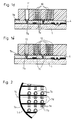
- FIG. 1 a shows schematically a section of a substrate in the form of a silicon wafer 1, on which an electronic circuit, symbolized by a MOSFET structure 2 and some conductor tracks 3, has been applied using known methods of semiconductor technology.
- the entire wafer with the circuits thereon is coated with an insulating protective layer 4 made of silicon nitride, into which, using known lithographic and etching methods of semiconductor production, contact openings 5, 6 for the connection surfaces of the sensor structure to be produced and for the external contacts of the circuit boards, over the corresponding locations of the circuits Circuits were created.
- a conductive layer of copper is sputtered onto this protective layer 4 and structured by means of lithographic and etching methods in such a way that a planarly structured electroplating electrode 7 is created in accordance with the layout of the sensor structures to be produced and the required conductor tracks and connections.
- PMMA positive X-ray resist
- the resist layer is partially irradiated with the X-rays of a synchrotron via an X-ray mask 9 (see arrows in FIG. 1c).
- X-ray mask 9 After the irradiated areas 8a have been detached, negatives 10, 11 of the sensor structures and the connection points are formed (FIG. 1d).
- the X-ray mask 9 must be adjusted so that the negatives 10, 11 that are formed are congruent with the previously structured galvanic electrode 7.
- copper is electrodeposited into the negatives 10, 11, the galvanic electrode 7 being contacted via the free annular edge 7a.
- the substrate is sawn into individual sensor chips.
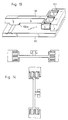
- FIG. 2 shows a top view of a section from the structured electroplating electrode 7 on the coated wafer 1, 4.
- the spiral-shaped parts 7c of the electrode 7 corresponding to the layout of the sensor structures are connected line by line to the ring-shaped edge 7a of the electroplating electrode, while the parts 7b corresponding to the outer contacts are connected to the next path.
- the existing electrical short-circuit connection between the outer connections of the circuit via the tracks 7d and the webs 7e running perpendicular thereto is interrupted (see section line 14).
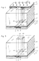
- FIG. 3 shows a perspective view and partially broken open schematically of the distance sensor thus produced with the spiral plate coil 12 as the sensor structure, the structured galvanic electrode 7 and the electronic circuits 2 covered by the insulating layer 4 on the silicon wafer 1. From the plate coil 12 with 50 turns a winding width and a winding spacing of 25 ⁇ m and a height of 250 ⁇ m, only a few turns are not shown to scale for technical reasons. The External contacting takes place via the column structures 13.
- the example shows that the method according to the invention is suitable for the mass production of sensors with inductively operating elements and with integrated signal processing.
- the geometry of the sensor structure can be freely selected in the lateral direction, considerably more complicated sensor structures can be realized than in this example, by combining characteristic dimensions in the micrometer range with a large structure height that is achieved for the sensor structures during production using the method according to the invention , the sensor structures can either be miniaturized with the same performance data or their performance data (eg the current carrying capacity) can be improved with the same geometry. Since a high precision of the geometry of the sensor structures is achieved with the method according to the invention and the problems associated with the connecting cables are eliminated due to the integrated structure, the complex adjustment and adjustment work can be omitted and the sensor element can be replaced with little effort in the event of defects.
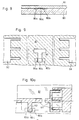
- FIG. 4 shows in perspective a section of a silicon wafer 41 on which an electronic circuit 44, the oxide layer 42 and the conductor tracks 43 have been produced using known methods of semiconductor technology.
- An insulating protective layer 45 for example made of silicon nitride, is applied to the wafer.
- the contact openings 46 for the coupling between the sensor structure and the circuit are produced by a lithography and etching step known from semiconductor technology.
- a conductive layer 47 covering the entire substrate is applied as a galvanic electrode made of, for example, nickel to the substrate provided with the protective layer 45.
- An approximately 1000 ⁇ m thick layer 48 of an X-ray resist is then applied.
- the resist layer 48 is exposed via an X-ray mask 49 with absorber structures 410 to the extremely parallel and intense radiation 411 from, for example, a synchrotron.
- the x-ray mask 49 is adjusted relative to the wafer 41 in such a way that the sensor structures to be produced are created over the corresponding contact openings 46.
- the areas 48a of the resist layer 48 which are not shadowed by the absorber structures 410 are changed by chemical radiation.
- the areas 48a of the resist layer 48 which are exposed to the radiation are detached during development, so that negatives 412 (FIG. 5) of the sensor structure are formed.
- a metal 413 e.g. Nickel, electroplated ( Figure 6).
- the remaining resist 48 is stripped and the exposed areas of the conductive layer 47 e.g. etched away dry ( Figure 7).
- the process concludes with the division of the wafer with the sensor structures applied to it into individual functional units (chips) with the help of e.g. a diamond circular saw along section line 414.
- the sensor structure manufactured in this way consists of a capacity of e.g. 1 pF, which is formed from a vibratable electrode in the form of a free-standing bar 413a with a height of approximately 1000 ⁇ m, a width of 350 ⁇ m and a thickness of 3 ⁇ m and a fixed counter electrode 413b.
- the vibratable electrode 413a is directly connected to the gate G e.g. a MOSFET circuit 44 connected.
- capacitive acceleration sensors can be produced with the method according to the invention, the sensitivity and measuring range of which can be optimally adapted to the particular use of the sensor. Due to the large selection of metals for the electrodes of the capacitance, an optimal adaptation of the vibration behavior (frequency range) to the respective application of the sensor is also possible.
- a capacitive acceleration sensor is described below, which is particularly well suited for measuring small accelerations.
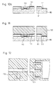
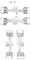
- the manufacture is based on a substrate 80 provided with an electronic circuit according to FIG. For reasons of better clarity, the further elements of the circuit and the connection contacts have been omitted.
- a polyimide layer 81 is applied to the substrate 80, which later serves as a removable intermediate layer between part of the sensor structures to be produced and the substrate.
- This layer 81 is structured using lithographic and etching methods in such a way that a T-shaped opening 90 is formed above the gate 80c of the MOS transistor and in a region adjoining it (FIG. 9). Further openings 91, 92 are structured so that they correspond to the outline of the comb-shaped counter electrodes of the sensor structure to be built.
- the intermediate polyimide layer 81 shown in FIG. 8 has not yet been removed.
- the depressions created in this way above the ground plan 111 are then galvanically filled with nickel, as a result of which the sensor structure embedded in the resist is formed in the form of electrodes 130, 131 which intermesh in a comb-like manner (FIG. 13).
- the substrate on which a multiplicity of such sensor structures are simultaneously built, is divided into individual chips.
- the remaining resist 120 (FIG. 12) is then removed and the polyimide intermediate layer 81 is chemically removed by means of an oxygen low-pressure plasma.
- one electrode 130 of the sensor structure has the shape of a bending beam with comb-shaped ends, the symmetrical construction of the bending beam only being firmly connected to the substrate 80 in its central region 130a, while the other regions are not touch and are therefore freely deflectable in the substrate plane.
- the counter electrode 131 is firmly connected to the substrate 80.
- the combs intertwine asymmetrically.
- the sensor arrangement described with a symmetrical bending beam has the advantage that very small translational accelerations can be measured independently of superimposed angular accelerations, the size of the angular acceleration can be of the same order of magnitude as the linear acceleration.
- the simultaneous measurement of linear and angular accelerations is also possible by producing two sensor arrangements parallel to one another on a common chip.
- the asymmetrical position of the combs with respect to one another is such that the arrangement 150 only responds to linear accelerations and is insensitive to angular accelerations.
- arrangement 151 it is the reverse, i.e. Angular accelerations are displayed, while with linear accelerations the changes in capacitance on the left and right side of the bending beam compensate for each other, i.e. they do not result in any display.
- the sensor structures can be constructed not only on the same side as the circuits, as described above, but also on the other side of the substrate. In the case of complex arrangements, both sides of the substrate can also be provided with sensor arrangements. In these cases, too, the spatially immediately adjacent manufacture of the sensor structures and the associated microcircuits coupled to them for integrated signal processing are realized.
- the resist material can be removed before or after dicing the substrate. Removal after cutting has the advantage that the sensitive sensor structures are embedded in the resist material and thus protected, and sawing is made easier.
Landscapes
- Physics & Mathematics (AREA)
- General Physics & Mathematics (AREA)
- Chemical & Material Sciences (AREA)
- Engineering & Computer Science (AREA)
- Chemical Kinetics & Catalysis (AREA)
- Electrochemistry (AREA)
- Materials Engineering (AREA)
- Metallurgy (AREA)
- Organic Chemistry (AREA)
- Pressure Sensors (AREA)
- Semiconductor Integrated Circuits (AREA)
- Measurement Of Radiation (AREA)
Abstract
Claims (5)
Priority Applications (1)
| Application Number | Priority Date | Filing Date | Title |
|---|---|---|---|
| AT88907108T ATE76199T1 (de) | 1987-08-14 | 1988-08-08 | Verfahren zur herstellung von mikrosensoren mit integrierter signalverarbeitung. |
Applications Claiming Priority (2)
| Application Number | Priority Date | Filing Date | Title |
|---|---|---|---|
| DE3727142A DE3727142C2 (de) | 1987-08-14 | 1987-08-14 | Verfahren zur Herstellung von Mikrosensoren mit integrierter Signalverarbeitung |
| DE3727142 | 1987-08-14 |
Publications (2)
| Publication Number | Publication Date |
|---|---|
| EP0371069A1 EP0371069A1 (fr) | 1990-06-06 |
| EP0371069B1 true EP0371069B1 (fr) | 1992-05-13 |
Family
ID=6333768
Family Applications (1)
| Application Number | Title | Priority Date | Filing Date |
|---|---|---|---|
| EP88907108A Expired - Lifetime EP0371069B1 (fr) | 1987-08-14 | 1988-08-08 | Procede de fabrication de microdetecteurs a traitement integre de signaux |
Country Status (5)
| Country | Link |
|---|---|
| US (1) | US5194402A (fr) |
| EP (1) | EP0371069B1 (fr) |
| JP (1) | JPH0693513B2 (fr) |
| DE (1) | DE3727142C2 (fr) |
| WO (1) | WO1989001632A1 (fr) |
Families Citing this family (39)
| Publication number | Priority date | Publication date | Assignee | Title |
|---|---|---|---|---|
| FI893874A7 (fi) * | 1989-08-17 | 1991-02-18 | Vaisala Oy | Kontaktfoersedd givare med skiktstruktur samt foerfarande foer utfoerande av kontakteringen. |
| DE3939112A1 (de) * | 1989-11-25 | 1991-05-29 | Kernforschungsz Karlsruhe | Vorrichtung zum positionieren von lichtleitfasern in verbindungselementen |
| DE4001399C1 (en) * | 1990-01-19 | 1991-07-25 | Kernforschungszentrum Karlsruhe Gmbh, 7500 Karlsruhe, De | Metallic microstructures - formed on substrates, by putting poly:methyl methacrylate] between moulding tool and silicon substrate |
| DE4024275A1 (de) * | 1990-07-31 | 1992-02-06 | Kernforschungsz Karlsruhe | Verfahren zur herstellung von mikrostrukturen mit bereichsweise unterschiedlicher strukturhoehe |
| DE4027732A1 (de) * | 1990-09-01 | 1992-03-05 | Thiedig Ullrich | Kamerachip fuer eine punktfoermige ereignisse erfassende und auswertende kamera |
| JPH04268725A (ja) * | 1991-02-25 | 1992-09-24 | Canon Inc | 力学量検出センサおよびその製造方法 |
| DE4126107C2 (de) * | 1991-08-07 | 1993-12-16 | Bosch Gmbh Robert | Beschleunigungssensor und Verfahren zur Herstellung |
| US6903084B2 (en) | 1991-08-28 | 2005-06-07 | Sterix Limited | Steroid sulphatase inhibitors |
| DE4226430C2 (de) * | 1992-08-10 | 1996-02-22 | Karlsruhe Forschzent | Kapazitiver Beschleunigungssensor |
| DE4304424C2 (de) * | 1993-02-13 | 1995-03-30 | Kernforschungsz Karlsruhe | Verfahren zum Herstellen von Mikrostrukturelementen auf einem Substrat, welche mit integrierten Schaltkreisen elektromechanisch, optisch oder elektrisch zusammenwirken |
| DE4310037C1 (de) * | 1993-03-27 | 1993-12-09 | Beermann Kg Martor Argentax | Messer mit verschiebbarer Messerklinge |
| US5616514A (en) * | 1993-06-03 | 1997-04-01 | Robert Bosch Gmbh | Method of fabricating a micromechanical sensor |
| DE4406342C1 (de) * | 1994-02-26 | 1995-03-09 | Kernforschungsz Karlsruhe | Sensor und Verfahren zu dessen Herstellung |
| DE4411130A1 (de) * | 1994-03-30 | 1995-10-05 | Siemens Ag | Sensoreinheit mit mindestens einem Beschleunigungssensor, z. B. zur Kfz-Airbagauslösung, und Verfahren zu seiner Herstellung |
| DE4418163B4 (de) * | 1994-05-25 | 2007-04-05 | Robert Bosch Gmbh | Verfahren zur Herstellung von mikromechanischen Strukturen |
| US5646348A (en) | 1994-08-29 | 1997-07-08 | The Charles Stark Draper Laboratory, Inc. | Micromechanical sensor with a guard band electrode and fabrication technique therefor |
| US5581035A (en) | 1994-08-29 | 1996-12-03 | The Charles Stark Draper Laboratory, Inc. | Micromechanical sensor with a guard band electrode |
| US5504026A (en) * | 1995-04-14 | 1996-04-02 | Analog Devices, Inc. | Methods for planarization and encapsulation of micromechanical devices in semiconductor processes |
| DE19522004A1 (de) * | 1995-06-21 | 1997-01-02 | Inst Mikrotechnik Mainz Gmbh | Herstellungsverfahren von teilbeweglichen Mikrostrukturen auf der Basis einer trockenchemisch geätzten Opferschicht |
| JPH09135032A (ja) * | 1995-11-08 | 1997-05-20 | Mitsubishi Electric Corp | 加速度検出用混成集積回路装置 |
| EP0822415B1 (fr) * | 1996-07-31 | 2003-03-26 | STMicroelectronics S.r.l. | Capteur d'accélération capacitif à semi-conducteur intégré et procédé pour sa fabrication |
| DE19641531A1 (de) * | 1996-10-09 | 1998-04-16 | Bosch Gmbh Robert | Mikromechanisches Bauelement und ein Verfahren zu dessen Herstellung |
| US5874356A (en) * | 1997-02-28 | 1999-02-23 | Taiwan Semiconductor Manufacturing Co. Ltd. | Method for forming zig-zag bordered openings in semiconductor structures |
| JP3187754B2 (ja) * | 1997-09-26 | 2001-07-11 | 富士電機株式会社 | 半導体センサおよびその製造方法 |
| DE19732250A1 (de) * | 1997-07-26 | 1999-01-28 | Bosch Gmbh Robert | Verfahren zur Herstellung metallischer Mikrostrukturen |
| KR100276387B1 (ko) * | 1998-01-08 | 2000-12-15 | 윤종용 | 반도체 장치의 자기정렬 콘택 형성 방법 |
| EP0969512B1 (fr) * | 1998-06-30 | 2009-05-13 | Asulab S.A. | Capteur inductif |
| DE59914876D1 (de) * | 1998-07-08 | 2008-11-06 | Infineon Technologies Ag | Verfahren zur herstellung einer integrierten schaltungsanordnung umfassend einen hohlraum in einer materialschicht, sowie eine durch das verfahren erzeugte integrierte schaltungsanordnung |
| DE19832905C2 (de) * | 1998-07-22 | 2000-06-29 | Karlsruhe Forschzent | Kapazitiver Beschleunigungssensor |
| US6278186B1 (en) | 1998-08-26 | 2001-08-21 | Intersil Corporation | Parasitic current barriers |
| JP2001005942A (ja) * | 1999-06-24 | 2001-01-12 | Shinko Electric Ind Co Ltd | Icカード及びその製造方法並びにアンテナ付き半導体装置及びその製造方法 |
| US6262463B1 (en) * | 1999-07-08 | 2001-07-17 | Integrated Micromachines, Inc. | Micromachined acceleration activated mechanical switch and electromagnetic sensor |
| DE19955975A1 (de) | 1999-11-19 | 2001-05-23 | Inst Mikrotechnik Mainz Gmbh | Lithographisches Verfahren zur Herstellung von Mikrobauteilen |
| US6720635B1 (en) | 1999-12-17 | 2004-04-13 | Motorola, Inc. | Electronic component |
| US7335650B2 (en) * | 2000-01-14 | 2008-02-26 | Sterix Limited | Composition |
| KR100543291B1 (ko) * | 2001-12-03 | 2006-01-20 | 주식회사 포스코 | 백업롤용 백업롤핀 |
| DE10161492C5 (de) * | 2001-12-14 | 2007-05-10 | Micromotion Gmbh | Verfahren zur Herstellung und Magazinierung von Mikrobauteilen, Magazin und Montageverfahren für Mikrobauteile |
| AU2002258715A1 (en) * | 2002-04-04 | 2003-10-20 | Illusion Technologies, Llc | Miniature/micro scale power generation system |
| DE10247487A1 (de) * | 2002-10-11 | 2004-05-06 | Infineon Technologies Ag | Membran und Verfahren zu deren Herstellung |
Family Cites Families (8)
| Publication number | Priority date | Publication date | Assignee | Title |
|---|---|---|---|---|
| DE2028819C3 (de) * | 1970-06-11 | 1980-05-29 | Siemens Ag, 1000 Berlin Und 8000 Muenchen | Verfahren zum Herstellen eines Metallkontakts mit einer Kontakthöhe > 10 µ m |
| US4078963A (en) * | 1973-12-10 | 1978-03-14 | U.S. Philips Corporation | Method of manufacturing a semiconductor device, having a pattern of conductors on a supporting body |
| US3993515A (en) * | 1975-03-31 | 1976-11-23 | Rca Corporation | Method of forming raised electrical contacts on a semiconductor device |
| US4436766A (en) * | 1981-05-15 | 1984-03-13 | The United States Of America As Represented By The Secretary Of The Navy | Plated bridge step-over connection for monolithic devices and method for making thereof |
| DE3204425A1 (de) * | 1982-02-09 | 1983-08-25 | Siemens AG, 1000 Berlin und 8000 München | Verfahren zur herstellung freitragender metallgitterstrukturen |
| DE3328899C2 (de) * | 1983-08-10 | 1985-07-11 | Nukem Gmbh, 6450 Hanau | Photovoltaische Zelle |
| JPH02277242A (ja) * | 1989-04-18 | 1990-11-13 | Nec Corp | 半導体装置の製造方法 |
| US4943539A (en) * | 1989-05-09 | 1990-07-24 | Motorola, Inc. | Process for making a multilayer metallization structure |
-
1987
- 1987-08-14 DE DE3727142A patent/DE3727142C2/de not_active Expired - Fee Related
-
1988
- 1988-08-08 JP JP63506552A patent/JPH0693513B2/ja not_active Expired - Lifetime
- 1988-08-08 US US07/340,175 patent/US5194402A/en not_active Expired - Lifetime
- 1988-08-08 WO PCT/DE1988/000488 patent/WO1989001632A1/fr not_active Ceased
- 1988-08-08 EP EP88907108A patent/EP0371069B1/fr not_active Expired - Lifetime
Non-Patent Citations (2)
| Title |
|---|
| Technische Rundschau, vol. 78, No. 35, August 1986, (Bern, CH), H. Benninghof: "Mikrostrukturtechnologie für innovative Produkte", pages 32-37 see pages 34-35, chapter: "Mikrofertigung nach dem LIGA-Verfahren"; pages 35-36, chapter: "Mikromechanik und siliziumtechnologie" * |
| Technische Rundschau, vol. 79, no. 13, 27 March 1987, (Bern, CH), E.-K. Aschmoneit: "LIGA: Mikrostrukturen, lithographisch hergestellt", pages 54-57 * |
Also Published As
| Publication number | Publication date |
|---|---|
| WO1989001632A1 (fr) | 1989-02-23 |
| JPH02500475A (ja) | 1990-02-15 |
| US5194402A (en) | 1993-03-16 |
| DE3727142A1 (de) | 1989-02-23 |
| EP0371069A1 (fr) | 1990-06-06 |
| JPH0693513B2 (ja) | 1994-11-16 |
| DE3727142C2 (de) | 1994-02-24 |
Similar Documents
| Publication | Publication Date | Title |
|---|---|---|
| EP0371069B1 (fr) | Procede de fabrication de microdetecteurs a traitement integre de signaux | |
| DE19619921B4 (de) | Verfahren zum Herstellen einer Halbleitervorrichtung mit Funktionselement und Schutzkappe | |
| EP0002185B1 (fr) | Procédé pour interconnecter deux conducteurs croisés se trouvant au-dessus de la surface d'un substrat | |
| DE68929150T2 (de) | Verfahren zur Herstellung einer Halbleitervorrichtung | |
| EP0721587B1 (fr) | Dispositif micromecanique et son procede de fabrication | |
| DE69305955T2 (de) | Beschleunigungssensor und seine herstellung | |
| DE3335772C2 (de) | Meßwandler und Verfahren zum Herstellen eines Meßwandlers, der auf Piezo-Widerstandsbasis arbeitet | |
| DE3343035C2 (de) | Verfahren zur Herstellung eines Magnetmeßfühlers mit mindestens zwei Elementen mit magnetischer Widerstandsänderung | |
| DE3900654C2 (de) | Drucksensoranordnung und Verfahren zu deren Herstellung | |
| EP0494143B1 (fr) | Dispositif pour mesurer des forces mecaniques et des effets dynamiques | |
| DE19719601A1 (de) | Beschleunigungssensor | |
| DE102012100007A1 (de) | Halbleitervorrichtungen mit Isoliersubstraten und Verfahren zur Bildung derselben | |
| DE102005005320A1 (de) | Magnetisches Sensorgerät und dessen Herstellungsverfahren | |
| DE102008007170A1 (de) | Beschleunigungssensor und Herstellungsverfahren desselben | |
| DE2315710B2 (de) | Verfahren zum Herstellen einer Halbleiteranordnung | |
| DE69514343T2 (de) | Halbleitereinrichtung mit einer mikrokomponente, die eine starre und eine bewegliche elektrode aufweist | |
| EP0167732B1 (fr) | Procédé pour la fabrication d'un matériau de base pour un circuit hybride | |
| EP0342274B1 (fr) | Agencement pour réduire des effets piézo dans un matériel semi-conducteur comportant au moins un dispositif électrique à effet piézo et son procédé de fabrication | |
| DE19819456B4 (de) | Verfahren zur Herstellung eines mikromechanischen Bauelements | |
| DE60025214T2 (de) | Mikrodeckelgehäuse auf Scheibenebene | |
| DE10019408C2 (de) | Feldeffekttransistor, insbesondere zur Verwendung als Sensorelement oder Beschleunigungssensor, und Verfahren zu dessen Herstellung | |
| DE2458410A1 (de) | Herstellungsverfahren fuer einen leistungshalbleiter mit presskontakten | |
| EP1522095A2 (fr) | Procede de production d'un composant a surfaces de connexion profondes | |
| EP2943988B1 (fr) | Procédé et dispositif de fabrication d'un système d'électrode multicouche | |
| EP1238311B1 (fr) | Bobine plate et procede lithographique pour produire des microcomposants |
Legal Events
| Date | Code | Title | Description |
|---|---|---|---|
| PUAI | Public reference made under article 153(3) epc to a published international application that has entered the european phase |
Free format text: ORIGINAL CODE: 0009012 |
|
| 17P | Request for examination filed |
Effective date: 19890519 |
|
| AK | Designated contracting states |
Kind code of ref document: A1 Designated state(s): AT BE CH DE FR GB IT LI LU NL SE |
|
| RBV | Designated contracting states (corrected) |
Designated state(s): AT CH FR GB IT LI NL SE |
|
| REG | Reference to a national code |
Ref country code: DE Ref legal event code: 8566 |
|
| 17Q | First examination report despatched |
Effective date: 19910926 |
|
| ITF | It: translation for a ep patent filed | ||
| GRAA | (expected) grant |
Free format text: ORIGINAL CODE: 0009210 |
|
| AK | Designated contracting states |
Kind code of ref document: B1 Designated state(s): AT CH FR GB IT LI NL SE |
|
| REF | Corresponds to: |
Ref document number: 76199 Country of ref document: AT Date of ref document: 19920515 Kind code of ref document: T |
|
| ET | Fr: translation filed | ||
| GBT | Gb: translation of ep patent filed (gb section 77(6)(a)/1977) | ||
| PLBE | No opposition filed within time limit |
Free format text: ORIGINAL CODE: 0009261 |
|
| STAA | Information on the status of an ep patent application or granted ep patent |
Free format text: STATUS: NO OPPOSITION FILED WITHIN TIME LIMIT |
|
| 26N | No opposition filed | ||
| EAL | Se: european patent in force in sweden |
Ref document number: 88907108.0 |
|
| PGFP | Annual fee paid to national office [announced via postgrant information from national office to epo] |
Ref country code: SE Payment date: 19970818 Year of fee payment: 10 |
|
| PGFP | Annual fee paid to national office [announced via postgrant information from national office to epo] |
Ref country code: AT Payment date: 19970826 Year of fee payment: 10 |
|
| PGFP | Annual fee paid to national office [announced via postgrant information from national office to epo] |
Ref country code: NL Payment date: 19970828 Year of fee payment: 10 |
|
| PGFP | Annual fee paid to national office [announced via postgrant information from national office to epo] |
Ref country code: FR Payment date: 19970829 Year of fee payment: 10 |
|
| PG25 | Lapsed in a contracting state [announced via postgrant information from national office to epo] |
Ref country code: AT Free format text: LAPSE BECAUSE OF NON-PAYMENT OF DUE FEES Effective date: 19980808 |
|
| PG25 | Lapsed in a contracting state [announced via postgrant information from national office to epo] |
Ref country code: SE Free format text: LAPSE BECAUSE OF NON-PAYMENT OF DUE FEES Effective date: 19980809 |
|
| PG25 | Lapsed in a contracting state [announced via postgrant information from national office to epo] |
Ref country code: NL Free format text: LAPSE BECAUSE OF NON-PAYMENT OF DUE FEES Effective date: 19990301 |
|
| PG25 | Lapsed in a contracting state [announced via postgrant information from national office to epo] |
Ref country code: FR Free format text: LAPSE BECAUSE OF NON-PAYMENT OF DUE FEES Effective date: 19990430 |
|
| EUG | Se: european patent has lapsed |
Ref document number: 88907108.0 |
|
| NLV4 | Nl: lapsed or anulled due to non-payment of the annual fee |
Effective date: 19990301 |
|
| REG | Reference to a national code |
Ref country code: FR Ref legal event code: ST |
|
| REG | Reference to a national code |
Ref country code: GB Ref legal event code: IF02 |
|
| PGFP | Annual fee paid to national office [announced via postgrant information from national office to epo] |
Ref country code: GB Payment date: 20050627 Year of fee payment: 18 |
|
| PGFP | Annual fee paid to national office [announced via postgrant information from national office to epo] |
Ref country code: CH Payment date: 20050722 Year of fee payment: 18 |
|
| PG25 | Lapsed in a contracting state [announced via postgrant information from national office to epo] |
Ref country code: IT Free format text: LAPSE BECAUSE OF NON-PAYMENT OF DUE FEES;WARNING: LAPSES OF ITALIAN PATENTS WITH EFFECTIVE DATE BEFORE 2007 MAY HAVE OCCURRED AT ANY TIME BEFORE 2007. THE CORRECT EFFECTIVE DATE MAY BE DIFFERENT FROM THE ONE RECORDED. Effective date: 20050808 |
|
| PG25 | Lapsed in a contracting state [announced via postgrant information from national office to epo] |
Ref country code: LI Free format text: LAPSE BECAUSE OF NON-PAYMENT OF DUE FEES Effective date: 20060831 Ref country code: CH Free format text: LAPSE BECAUSE OF NON-PAYMENT OF DUE FEES Effective date: 20060831 |
|
| REG | Reference to a national code |
Ref country code: CH Ref legal event code: PL |
|
| GBPC | Gb: european patent ceased through non-payment of renewal fee |
Effective date: 20060808 |
|
| PG25 | Lapsed in a contracting state [announced via postgrant information from national office to epo] |
Ref country code: GB Free format text: LAPSE BECAUSE OF NON-PAYMENT OF DUE FEES Effective date: 20060808 |