EP0371069B1 - Process for manufacturing microsensors with integrated signal processing - Google Patents
Process for manufacturing microsensors with integrated signal processing Download PDFInfo
- Publication number
- EP0371069B1 EP0371069B1 EP88907108A EP88907108A EP0371069B1 EP 0371069 B1 EP0371069 B1 EP 0371069B1 EP 88907108 A EP88907108 A EP 88907108A EP 88907108 A EP88907108 A EP 88907108A EP 0371069 B1 EP0371069 B1 EP 0371069B1
- Authority
- EP
- European Patent Office
- Prior art keywords
- substrate
- layer
- sensor structures
- sensor
- produced
- Prior art date
- Legal status (The legal status is an assumption and is not a legal conclusion. Google has not performed a legal analysis and makes no representation as to the accuracy of the status listed.)
- Expired - Lifetime
Links
Images


Classifications
-
- G—PHYSICS
- G01—MEASURING; TESTING
- G01P—MEASURING LINEAR OR ANGULAR SPEED, ACCELERATION, DECELERATION, OR SHOCK; INDICATING PRESENCE, ABSENCE, OR DIRECTION, OF MOVEMENT
- G01P15/00—Measuring acceleration; Measuring deceleration; Measuring shock, i.e. sudden change of acceleration
- G01P15/02—Measuring acceleration; Measuring deceleration; Measuring shock, i.e. sudden change of acceleration by making use of inertia forces using solid seismic masses
- G01P15/08—Measuring acceleration; Measuring deceleration; Measuring shock, i.e. sudden change of acceleration by making use of inertia forces using solid seismic masses with conversion into electric or magnetic values
- G01P15/0802—Details
-
- C—CHEMISTRY; METALLURGY
- C25—ELECTROLYTIC OR ELECTROPHORETIC PROCESSES; APPARATUS THEREFOR
- C25D—PROCESSES FOR THE ELECTROLYTIC OR ELECTROPHORETIC PRODUCTION OF COATINGS; ELECTROFORMING; APPARATUS THEREFOR
- C25D7/00—Electroplating characterised by the article coated
- C25D7/12—Semiconductors
- C25D7/123—Semiconductors first coated with a seed layer or a conductive layer
-
- G—PHYSICS
- G01—MEASURING; TESTING
- G01P—MEASURING LINEAR OR ANGULAR SPEED, ACCELERATION, DECELERATION, OR SHOCK; INDICATING PRESENCE, ABSENCE, OR DIRECTION, OF MOVEMENT
- G01P15/00—Measuring acceleration; Measuring deceleration; Measuring shock, i.e. sudden change of acceleration
- G01P15/02—Measuring acceleration; Measuring deceleration; Measuring shock, i.e. sudden change of acceleration by making use of inertia forces using solid seismic masses
- G01P15/08—Measuring acceleration; Measuring deceleration; Measuring shock, i.e. sudden change of acceleration by making use of inertia forces using solid seismic masses with conversion into electric or magnetic values
- G01P15/125—Measuring acceleration; Measuring deceleration; Measuring shock, i.e. sudden change of acceleration by making use of inertia forces using solid seismic masses with conversion into electric or magnetic values by capacitive pick-up
-
- G—PHYSICS
- G03—PHOTOGRAPHY; CINEMATOGRAPHY; ANALOGOUS TECHNIQUES USING WAVES OTHER THAN OPTICAL WAVES; ELECTROGRAPHY; HOLOGRAPHY
- G03F—PHOTOMECHANICAL PRODUCTION OF TEXTURED OR PATTERNED SURFACES, e.g. FOR PRINTING, FOR PROCESSING OF SEMICONDUCTOR DEVICES; MATERIALS THEREFOR; ORIGINALS THEREFOR; APPARATUS SPECIALLY ADAPTED THEREFOR
- G03F7/00—Photomechanical, e.g. photolithographic, production of textured or patterned surfaces, e.g. printing surfaces; Materials therefor, e.g. comprising photoresists; Apparatus specially adapted therefor
-
- G—PHYSICS
- G01—MEASURING; TESTING
- G01P—MEASURING LINEAR OR ANGULAR SPEED, ACCELERATION, DECELERATION, OR SHOCK; INDICATING PRESENCE, ABSENCE, OR DIRECTION, OF MOVEMENT
- G01P15/00—Measuring acceleration; Measuring deceleration; Measuring shock, i.e. sudden change of acceleration
- G01P15/02—Measuring acceleration; Measuring deceleration; Measuring shock, i.e. sudden change of acceleration by making use of inertia forces using solid seismic masses
- G01P15/08—Measuring acceleration; Measuring deceleration; Measuring shock, i.e. sudden change of acceleration by making use of inertia forces using solid seismic masses with conversion into electric or magnetic values
- G01P2015/0805—Measuring acceleration; Measuring deceleration; Measuring shock, i.e. sudden change of acceleration by making use of inertia forces using solid seismic masses with conversion into electric or magnetic values being provided with a particular type of spring-mass-system for defining the displacement of a seismic mass due to an external acceleration
- G01P2015/0808—Measuring acceleration; Measuring deceleration; Measuring shock, i.e. sudden change of acceleration by making use of inertia forces using solid seismic masses with conversion into electric or magnetic values being provided with a particular type of spring-mass-system for defining the displacement of a seismic mass due to an external acceleration for defining in-plane movement of the mass, i.e. movement of the mass in the plane of the substrate
- G01P2015/0811—Measuring acceleration; Measuring deceleration; Measuring shock, i.e. sudden change of acceleration by making use of inertia forces using solid seismic masses with conversion into electric or magnetic values being provided with a particular type of spring-mass-system for defining the displacement of a seismic mass due to an external acceleration for defining in-plane movement of the mass, i.e. movement of the mass in the plane of the substrate for one single degree of freedom of movement of the mass
- G01P2015/0817—Measuring acceleration; Measuring deceleration; Measuring shock, i.e. sudden change of acceleration by making use of inertia forces using solid seismic masses with conversion into electric or magnetic values being provided with a particular type of spring-mass-system for defining the displacement of a seismic mass due to an external acceleration for defining in-plane movement of the mass, i.e. movement of the mass in the plane of the substrate for one single degree of freedom of movement of the mass for pivoting movement of the mass, e.g. in-plane pendulum
-
- Y—GENERAL TAGGING OF NEW TECHNOLOGICAL DEVELOPMENTS; GENERAL TAGGING OF CROSS-SECTIONAL TECHNOLOGIES SPANNING OVER SEVERAL SECTIONS OF THE IPC; TECHNICAL SUBJECTS COVERED BY FORMER USPC CROSS-REFERENCE ART COLLECTIONS [XRACs] AND DIGESTS
- Y10—TECHNICAL SUBJECTS COVERED BY FORMER USPC
- Y10S—TECHNICAL SUBJECTS COVERED BY FORMER USPC CROSS-REFERENCE ART COLLECTIONS [XRACs] AND DIGESTS
- Y10S438/00—Semiconductor device manufacturing: process
- Y10S438/942—Masking
- Y10S438/948—Radiation resist
Definitions
- the invention relates to a method for producing microsensors with integrated signal processing according to the preamble of patent claim 1.
- microsensors of the generic type it is known to combine methods of semiconductor technology and anisotropic silicon etching technology with one another in order to produce the electronic circuits and the sensor structures coupled to them on a silicon wafer in a production sequence.
- Such a procedure for producing a capacitive acceleration sensor is described in KE Petersen, A. Shartel and NF Raley "Micromechanical Accelerometer Integrated with MOS Detection Circuitry", IEE Transactions on Electron Devices, Vol. ED-29, No. January 1, 1982, pp. 23 to 27, described and shown.
- FIG. 1 of this publication a structured p-doped layer is first produced in the surface of a Si wafer as the electrode and etch stop layer.
- Silicon is then epitaxially deposited to a thickness corresponding to the electrode spacing and a structured silicon oxide layer is produced.
- a contact hole is made through the epitaxial silicon layer to the buried electrode through the opening in the silicon oxide layer using anisotropic etching technology.
- the source and drain regions and the electrical connection in the contact hole are produced by doping.
- the gate oxide is then generated and an etching window is exposed in the silicon oxide layer for later formation of the sensor structure in the form of a tongue.
- the electrical connections are then made and the tongue area is metallized.
- the last step is through anisotropic silicon etching a pit is formed between the buried electrode and the silicon oxide, which creates a vibratable tongue made of metallized silicon oxide.
- a disadvantage of this production sequence is that standard semiconductor processes such as, for example, oxidation and doping are used in alternating sequences with anisotropic silicon etching processes. This leads to problems in series production, since the use of alkaline etchants in anisotropic etching poses the risk that the properties of the electronic circuits are undesirably changed.
- the object of the invention is to provide a method for producing microsensors of the generic type, in which the production steps for the sensor structures have no negative effects on the electronic circuits coupled to them.
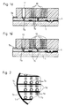
- FIG. 1 a shows schematically a section of a substrate in the form of a silicon wafer 1, on which an electronic circuit, symbolized by a MOSFET structure 2 and some conductor tracks 3, has been applied using known methods of semiconductor technology.
- the entire wafer with the circuits thereon is coated with an insulating protective layer 4 made of silicon nitride, into which, using known lithographic and etching methods of semiconductor production, contact openings 5, 6 for the connection surfaces of the sensor structure to be produced and for the external contacts of the circuit boards, over the corresponding locations of the circuits Circuits were created.
- a conductive layer of copper is sputtered onto this protective layer 4 and structured by means of lithographic and etching methods in such a way that a planarly structured electroplating electrode 7 is created in accordance with the layout of the sensor structures to be produced and the required conductor tracks and connections.
- PMMA positive X-ray resist
- the resist layer is partially irradiated with the X-rays of a synchrotron via an X-ray mask 9 (see arrows in FIG. 1c).
- X-ray mask 9 After the irradiated areas 8a have been detached, negatives 10, 11 of the sensor structures and the connection points are formed (FIG. 1d).
- the X-ray mask 9 must be adjusted so that the negatives 10, 11 that are formed are congruent with the previously structured galvanic electrode 7.
- copper is electrodeposited into the negatives 10, 11, the galvanic electrode 7 being contacted via the free annular edge 7a.
- the substrate is sawn into individual sensor chips.
- FIG. 2 shows a top view of a section from the structured electroplating electrode 7 on the coated wafer 1, 4.
- the spiral-shaped parts 7c of the electrode 7 corresponding to the layout of the sensor structures are connected line by line to the ring-shaped edge 7a of the electroplating electrode, while the parts 7b corresponding to the outer contacts are connected to the next path.
- the existing electrical short-circuit connection between the outer connections of the circuit via the tracks 7d and the webs 7e running perpendicular thereto is interrupted (see section line 14).
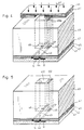
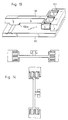
- FIG. 3 shows a perspective view and partially broken open schematically of the distance sensor thus produced with the spiral plate coil 12 as the sensor structure, the structured galvanic electrode 7 and the electronic circuits 2 covered by the insulating layer 4 on the silicon wafer 1. From the plate coil 12 with 50 turns a winding width and a winding spacing of 25 ⁇ m and a height of 250 ⁇ m, only a few turns are not shown to scale for technical reasons. The External contacting takes place via the column structures 13.
- the example shows that the method according to the invention is suitable for the mass production of sensors with inductively operating elements and with integrated signal processing.
- the geometry of the sensor structure can be freely selected in the lateral direction, considerably more complicated sensor structures can be realized than in this example, by combining characteristic dimensions in the micrometer range with a large structure height that is achieved for the sensor structures during production using the method according to the invention , the sensor structures can either be miniaturized with the same performance data or their performance data (eg the current carrying capacity) can be improved with the same geometry. Since a high precision of the geometry of the sensor structures is achieved with the method according to the invention and the problems associated with the connecting cables are eliminated due to the integrated structure, the complex adjustment and adjustment work can be omitted and the sensor element can be replaced with little effort in the event of defects.
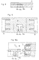
- FIG. 4 shows in perspective a section of a silicon wafer 41 on which an electronic circuit 44, the oxide layer 42 and the conductor tracks 43 have been produced using known methods of semiconductor technology.
- An insulating protective layer 45 for example made of silicon nitride, is applied to the wafer.
- the contact openings 46 for the coupling between the sensor structure and the circuit are produced by a lithography and etching step known from semiconductor technology.
- a conductive layer 47 covering the entire substrate is applied as a galvanic electrode made of, for example, nickel to the substrate provided with the protective layer 45.
- An approximately 1000 ⁇ m thick layer 48 of an X-ray resist is then applied.
- the resist layer 48 is exposed via an X-ray mask 49 with absorber structures 410 to the extremely parallel and intense radiation 411 from, for example, a synchrotron.
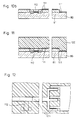
- the x-ray mask 49 is adjusted relative to the wafer 41 in such a way that the sensor structures to be produced are created over the corresponding contact openings 46.
- the areas 48a of the resist layer 48 which are not shadowed by the absorber structures 410 are changed by chemical radiation.
- the areas 48a of the resist layer 48 which are exposed to the radiation are detached during development, so that negatives 412 (FIG. 5) of the sensor structure are formed.
- a metal 413 e.g. Nickel, electroplated ( Figure 6).
- the remaining resist 48 is stripped and the exposed areas of the conductive layer 47 e.g. etched away dry ( Figure 7).
- the process concludes with the division of the wafer with the sensor structures applied to it into individual functional units (chips) with the help of e.g. a diamond circular saw along section line 414.
- the sensor structure manufactured in this way consists of a capacity of e.g. 1 pF, which is formed from a vibratable electrode in the form of a free-standing bar 413a with a height of approximately 1000 ⁇ m, a width of 350 ⁇ m and a thickness of 3 ⁇ m and a fixed counter electrode 413b.
- the vibratable electrode 413a is directly connected to the gate G e.g. a MOSFET circuit 44 connected.
- capacitive acceleration sensors can be produced with the method according to the invention, the sensitivity and measuring range of which can be optimally adapted to the particular use of the sensor. Due to the large selection of metals for the electrodes of the capacitance, an optimal adaptation of the vibration behavior (frequency range) to the respective application of the sensor is also possible.
- a capacitive acceleration sensor is described below, which is particularly well suited for measuring small accelerations.
- the manufacture is based on a substrate 80 provided with an electronic circuit according to FIG. For reasons of better clarity, the further elements of the circuit and the connection contacts have been omitted.
- a polyimide layer 81 is applied to the substrate 80, which later serves as a removable intermediate layer between part of the sensor structures to be produced and the substrate.
- This layer 81 is structured using lithographic and etching methods in such a way that a T-shaped opening 90 is formed above the gate 80c of the MOS transistor and in a region adjoining it (FIG. 9). Further openings 91, 92 are structured so that they correspond to the outline of the comb-shaped counter electrodes of the sensor structure to be built.
- the intermediate polyimide layer 81 shown in FIG. 8 has not yet been removed.
- the depressions created in this way above the ground plan 111 are then galvanically filled with nickel, as a result of which the sensor structure embedded in the resist is formed in the form of electrodes 130, 131 which intermesh in a comb-like manner (FIG. 13).
- the substrate on which a multiplicity of such sensor structures are simultaneously built, is divided into individual chips.
- the remaining resist 120 (FIG. 12) is then removed and the polyimide intermediate layer 81 is chemically removed by means of an oxygen low-pressure plasma.
- one electrode 130 of the sensor structure has the shape of a bending beam with comb-shaped ends, the symmetrical construction of the bending beam only being firmly connected to the substrate 80 in its central region 130a, while the other regions are not touch and are therefore freely deflectable in the substrate plane.
- the counter electrode 131 is firmly connected to the substrate 80.
- the combs intertwine asymmetrically.
- the sensor arrangement described with a symmetrical bending beam has the advantage that very small translational accelerations can be measured independently of superimposed angular accelerations, the size of the angular acceleration can be of the same order of magnitude as the linear acceleration.
- the simultaneous measurement of linear and angular accelerations is also possible by producing two sensor arrangements parallel to one another on a common chip.
- the asymmetrical position of the combs with respect to one another is such that the arrangement 150 only responds to linear accelerations and is insensitive to angular accelerations.
- arrangement 151 it is the reverse, i.e. Angular accelerations are displayed, while with linear accelerations the changes in capacitance on the left and right side of the bending beam compensate for each other, i.e. they do not result in any display.
- the sensor structures can be constructed not only on the same side as the circuits, as described above, but also on the other side of the substrate. In the case of complex arrangements, both sides of the substrate can also be provided with sensor arrangements. In these cases, too, the spatially immediately adjacent manufacture of the sensor structures and the associated microcircuits coupled to them for integrated signal processing are realized.
- the resist material can be removed before or after dicing the substrate. Removal after cutting has the advantage that the sensitive sensor structures are embedded in the resist material and thus protected, and sawing is made easier.
Landscapes
- Physics & Mathematics (AREA)
- General Physics & Mathematics (AREA)
- Chemical & Material Sciences (AREA)
- Engineering & Computer Science (AREA)
- Chemical Kinetics & Catalysis (AREA)
- Electrochemistry (AREA)
- Materials Engineering (AREA)
- Metallurgy (AREA)
- Organic Chemistry (AREA)
- Pressure Sensors (AREA)
- Semiconductor Integrated Circuits (AREA)
- Measurement Of Radiation (AREA)
Abstract
Description
Die Erfindung betrifft ein Verfahren zur Herstellung von Mikrosensoren mit integrierter Signalverarbeitung gemäß dem Oberbegriff von Patentanspruch 1.The invention relates to a method for producing microsensors with integrated signal processing according to the preamble of
Zur Herstellung von Mikrosensoren gattungsgemäßen Art ist es bekanntt, Methoden der Halbleitertechnik und der anisotropen Siliziumätztechnik miteinander zu kombinieren, um in einer Fertigungsfolge die elektronischen Schaltkreise und die damit gekoppelten Sensorstrukturen auf einem Siliziumwafer herzustellen. Eine derartige Vorgehensweise zur Herstellung eines kapazitiven Beschleunigungssensors ist in K.E. Petersen, A. Shartel and N.F. Raley "Micromechanical Accelerometer Integrated with MOS Detection Circuitry", IEE Transactions on Electron Devices, Vol. ED-29, No. 1, January 1982, pp. 23 to 27, beschrieben und dargestellt. Gemäß Figur 1 dieser Veröffentlichung wird zunächst als Elektrode und Ätzstoppschicht eine strukturierte p-dotierte Schicht in der Oberfläche eines Si-Wafers erzeugt. Sodann wird epitaktisch Silizium in einer dem Elektrodenabstand entsprechenden Dicke abgeschieden und eine strukturierte Siliziumoxidschicht erzeugt. Durch die Öffnung in der Siliziumoxidschicht wird mittels anisotroper Ätztechnik ein Kontaktloch durch die epitaktische Siliziumschicht zur vergrabenen Elektrode hergestellt. Durch Dotieren werden Source- und Drainbereich und die elektrische Verbindung im Kontaktloch erzeugt. Danach wird das Gateoxid erzeugt und ein Ätzfenster in der Siliziumoxidschicht zur späteren Bildung der Sensorstruktur in Form einer Zunge freigelegt. Sodann werden die elektrischen Verbindungen erzeugt und der Zungenbereich metallisiert. Als letzter Schritt wird durch anisotropes Siliziumätzen eine Grube zwischen der vergrabenen Elektrode und dem Siliziumoxid gebildet, wodurch eine schwingfähige Zunge aus metallisiertem Siliziumoxid entsteht. Nachteilig bei dieser Fertigungsfolge wirkt sich aus, daß Standardhalbbleiterprozesse wie z.B. das Oxidieren und das Dotieren in wechselnder Folge mit anisotropen Siliziumätzprozessen angewendet werden. Dies führt zu Problemen bei der Serienfertigung, da durch die Verwendung alkalischer Ätzmittel beim anisotropen Ätzen die Gefahr besteht, daß die Eigenschaften der elektronischen Schaltkreise in unerwünschter Weise verändert werden.For the production of microsensors of the generic type, it is known to combine methods of semiconductor technology and anisotropic silicon etching technology with one another in order to produce the electronic circuits and the sensor structures coupled to them on a silicon wafer in a production sequence. Such a procedure for producing a capacitive acceleration sensor is described in KE Petersen, A. Shartel and NF Raley "Micromechanical Accelerometer Integrated with MOS Detection Circuitry", IEE Transactions on Electron Devices, Vol. ED-29, No. January 1, 1982, pp. 23 to 27, described and shown. According to FIG. 1 of this publication, a structured p-doped layer is first produced in the surface of a Si wafer as the electrode and etch stop layer. Silicon is then epitaxially deposited to a thickness corresponding to the electrode spacing and a structured silicon oxide layer is produced. A contact hole is made through the epitaxial silicon layer to the buried electrode through the opening in the silicon oxide layer using anisotropic etching technology. The source and drain regions and the electrical connection in the contact hole are produced by doping. The gate oxide is then generated and an etching window is exposed in the silicon oxide layer for later formation of the sensor structure in the form of a tongue. The electrical connections are then made and the tongue area is metallized. The last step is through anisotropic silicon etching a pit is formed between the buried electrode and the silicon oxide, which creates a vibratable tongue made of metallized silicon oxide. A disadvantage of this production sequence is that standard semiconductor processes such as, for example, oxidation and doping are used in alternating sequences with anisotropic silicon etching processes. This leads to problems in series production, since the use of alkaline etchants in anisotropic etching poses the risk that the properties of the electronic circuits are undesirably changed.
Die Erfindung hat zur Aufgabe, ein Verfahren zur Herstellung von Mikrosensoren der gattungsgemäßen Art zur Verfügung zu stellen, bei dem die Herstellungsschritte für die Sensorstrukturen keine negativen Auswirkungen auf die damit gekoppelten elektronischen Schaltkreise haben.The object of the invention is to provide a method for producing microsensors of the generic type, in which the production steps for the sensor structures have no negative effects on the electronic circuits coupled to them.
Zur Lösung dieser Aufgabe werden die im Kennzeichen von Anspruch 1 enthaltenen Verfahrensschritte vorgeschlagen. Die hierauf bezogenen Unteransprüche beinhalten vorteilhafte Ausgestaltungen dieser Lösung.To achieve this object, the method steps contained in the characterizing part of
Die Herstellung von Mikrostrukturen auf röntgenlithographischem Wege (LIGA-Verfahren) ist in der Zeitschrift "Technische Rundschau" (T.R.) 78, 1986, No. 35, Seiten 34, 35 undT.R. 79 (1987), No. 13, Seiten 54 bis 57 beschrieben. In T.R.78 (1986), No. 35, Seite 34 wird u.a. auf die Anwendungsmöglichkeit des LIGA-Verfahrens bei der Sensortechnik hingewiesen. Die Gesamtkombination der Verfahrensschritte von Anspruch 1 zur Herstellung gattungsgemäßer Mikrosensoren mit integrierter Signalverarbeitung ist aus diesen Veröffentlichungen jedoch nicht herleitbar.The production of microstructures by X-ray lithography (LIGA method) is described in the journal "Technische Rundschau" (T.R.) 78, 1986, No. 35, pages 34, 35 and T.R. 79 (1987), No. 13, pages 54 to 57. In T.R.78 (1986), No. 35, page 34 includes pointed out the possibility of using the LIGA method in sensor technology. However, the total combination of the method steps of
Das erfindungsgemäße Verfahren hat den Vorteil, daß die Herstellung der Sensorstrukturen unabhängig von der Herstellung der elektronischen Schaltkreise ist und letztere nicht beinflußt. Ausführungsbeispiele der Erfindung werden im folgenden anhand der Zeichnungen erläutert:
Figuren 1 bis 3 zeigen die Herstellung eines induktiven Abstandssensors nach dem erfindungsgemäßen Verfahren,Figuren 4 bis 7 zeigen die Herstellung eines kapazitiven Beschleunigungssensors,Figuren 8 bis 15 zeigen die Herstellung eines kapazitiven Beschleunigungssensors für die Messung sehr kleiner Beschleunigungen.
- FIGS. 1 to 3 show the manufacture of an inductive distance sensor using the method according to the invention,
- FIGS. 4 to 7 show the production of a capacitive acceleration sensor,
- FIGS. 8 to 15 show the production of a capacitive acceleration sensor for measuring very small accelerations.
Figur 1a zeigt schematisch einen Ausschnitt eines Substrats in Form eines Siliziumwafers 1, auf dem ein elektronischer Schaltkreis, symbolisiert durch eine MOSFET-Struktur 2 und einige Leiterbahnen 3, nach bekannten Methoden der Halbleitertechnik aufgebracht wurde.FIG. 1 a shows schematically a section of a substrate in the form of a
Der gesamte Wafer mit darauf befindlichen Schaltkreisen wird mit einer isolierenden Schutzschicht 4 aus Siliziumnitrid überzogen, in die unter Anwendung bekannter lithographischer und ätztechnischer Methoden der Halbleiterfertigung über den entsprechenden Stellen der Schaltkreise Kontaktöffnungen 5,6 für die Anschlußflächen der herzustellenden Sensorstruktur und für die externen Kontakte der Schaltkreise erzeugt wurden.The entire wafer with the circuits thereon is coated with an insulating
Gemäß Figur 1b wird auf diese Schutzschicht 4 eine leitfähige Schicht aus Kupfer aufgesputtert und mittels lithographischer und ätztechnischer Methoden so strukturiert, daß nach Maßgabe des Grundrisses der herzustellenden Sensorstrukturen sowie der erforderlichen Leiterbahnen und Anschlüsse eine flächenhaft strukturierte Galvanikelektrode 7 entsteht.According to FIG. 1b, a conductive layer of copper is sputtered onto this
Sodann wird der gesamte Wafer 1 mit Ausnahme des verkupferten ringförmigen Randes 7a mit einer 300 µm dicken Schicht 8 eines Positiv-Röntgenresists (PMMA) beschichtet.Then the
Über eine Röntgenmaske 9 wird die Resistschicht mit der Röntgenstrahlung eines Synchrotrons partiell bestrahlt (s.Pfeile in Figur 1c). Nach dem Herauslösen der bestrahlten Bereiche 8a entstehen Negative 10, 11 der Sensorstrukturen und der Anschlußpunkte (Figur 1d). Hierzu muß die Röntgenmaske 9 so justiert werden, daß die entstehenden Negative 10, 11 kongruent zur zuvor strukturierten Galvanikelektrode 7 sind. Hierauf wird in die Negative 10, 11 galvanisch Kupfer abgeschieden, wobei die Galvanikelektrode 7 über dem freigehaltenen ringförmigen Rand 7a kontaktiert wird. Nach Überfräsen des Resists mit den darin eingebetteten Kupferstrukturen 12, 13 (Figur 1e) auf eine Solldicke von 250 µm wird das Substrat in einzelne Sensorchips zersägt.The resist layer is partially irradiated with the X-rays of a synchrotron via an X-ray mask 9 (see arrows in FIG. 1c). After the
In der Figur 2 ist in der Draufsicht ein Ausschnitt aus der strukturierten Galvanikelektrode 7 auf dem beschichteten Wafer 1,4 gezeigt. Die dem Grundriß der Sensorstrukturen entsprechenden spiralförmigen Teile 7c der Elektrode 7 sind über Bahnen 7d zeilenweise mit dem ringförmigen Rand 7a der Galvanikelektrode verbunden, während die den äußeren Kontakten entsprechenden Teile 7b mit der jeweils nächsten Bahn verbunden sind. Beim Aufteilen in die einzelnen Chips wird die über die Bahnen 7d und die hierzu senkrecht verlaufenden Stege 7e bestehende elektrische Kurzschlußverbindung zwischen den äußeren Anschlüssen der Schaltung unterbrochen (s. Schnittlinie 14).FIG. 2 shows a top view of a section from the structured
Die Figur 3 zeigt in perspektivischer Ansicht und teilweise aufgerissen schematisch den so hergestellten Abstandssensor mit der spiralförmigen Tellerspule 12 als Sensorstruktur, der strukturierten Galvanikelektrode 7 und die von der Isolierschicht 4 überdeckten elektronischen Schaltkreise 2 auf dem Siliziumwafer 1. Von der Tellerspule 12 mit 50 Windungen mit einer Windungsbreite und einem Windungsabstand von je 25 µm und einer Höhe von 250 µm sind aus darstellungstechnischen Gründen nur wenige Windungen nicht maßstabsgemäß gezeigt. Die externe Kontaktierung erfolgt über die Säulenstrukturen 13. Das Beispiel zeigt, daß das erfindungsgemäße Verfahren zur Massenfertigung von Sensoren mit induktiv arbeitenden Elementen und mit integrierter Signalverarbeitung geeignet ist. Da die Geometrie der Sensorstruktur in lateraler Richtung frei wählbar ist, lassen sich auch erheblich kompliziertere Sensorstrukturen als in diesem Beispiel realisieren.Durch die Kombination von charakteristischen Abmessungen im Mikrometerbereich mit einer großen Strukturhöhe, die bei der Fertigung nach dem erfindungsgemäßen Verfahren für die Sensorstrukturen erreicht wird, können die Sensorstrukturen entweder bei gleichen Leistungsdaten miniaturisiert oder bei gleicher Geometrie in ihren Leistungsdaten (z.B. der Strombelastbarkeit) verbessert werden. Da mit dem erfindungsgemäßen Verfahren eine hohe Präzision der Geometrie der Sensorstrukturen erreicht wird und durch den integrierten Aufbau die mit den Anschlußkabeln verbundene Problematik entfällt, können die aufwendigen Abgleichsund Justierarbeiten entfallen, und das Sensorelement kann bei Defekten mit geringem Aufwand ausgetauscht werden.FIG. 3 shows a perspective view and partially broken open schematically of the distance sensor thus produced with the
Die Figur 4 zeigt perspektivisch einen Ausschnitt eines Siliziumwafers 41, auf dem nach bekannten Methoden der Halbleitertechnik ein elektronischer Schaltkreis 44, die Oxidschicht 42 und die Leiterbahnen 43 gefertigt wurden. Auf den Wafer wird eine isolierende Schutzschicht 45, z.B. aus Siliziumnitrid, aufgebracht. Durch einen aus der Halbleitertechnik bekannten Lithographie- und Ätzschritt werden die Kontaktöffnungen 46 für die Kopplung zwischen Sensorstruktur und Schaltkreis erzeugt. Nunmehr wird z.B. durch Aufdampfen eine das gesamte Substrat überdeckende Leitschicht 47 als Galvanikelektrode aus z.B. Nickel auf das mit der Schutzschicht 45 versehene Substrat aufgebracht. Sodann erfolgt das Aufbringen einer etwa 1000 µm dicken Schicht 48 eines Röntgenresists. Die Resistschicht 48 wird über eine Röntgenmaske 49 mit Absorberstrukturen 410 mit der extrem parallelen und intensiven Strahlung 411 aus z.B. einem Synchrotron belichtet.FIG. 4 shows in perspective a section of a
Die Röntgenmaske 49 wird dabei so zum Wafer 41 justiert, daß die herzustellenden Sensorstrukturen über den entsprechenden Kontaktöffnungen 46 entstehen. Bei der Bestrahlung werden die Bereiche 48a der Resistschicht 48, die nicht von den Absorberstrukturen 410 abgeschattet werden, strahlenchemisch verändert. Nach der Bestrahlung werden beim Entwickeln die der Strahlung ausgesetzten Bereiche 48a der Resistschicht 48 herausgelöst, so daß Negative 412 (Figur 5) der Sensorstruktur entstehen. In diese Negative 412 wird unter Verwendung der Leitschicht 47 als Galvanikelektrode ein Metall 413, z.B. Nickel, galvanisch abgeschieden (Figur 6). Nach der Herstellung der metallischen Sensorstrukturen 413 werden der restliche Resist 48 gestrippt und die freigelegten Bereiche der Leitschicht 47 z.B. trocken weggeätzt (Figur 7). Der Prozeß schließt mit dem Aufteilen des Wafers mit den darauf aufgebrachten Sensorstrukturen in einzelne Funktionseinheiten (Chips) mit Hilfe z.B. einer Diamantkreissäge entlang der Schnittlinie 414.The
Die so gefertigte Sensorstruktur besteht aus einer Kapazität von z.B. 1 pF, die aus einer schwingfähigen Elektrode in Form eines freistehenden Balkens 413a mit einer Höhe von etwa 1000 µm, einer Breite von 350 µm und einer Dicke von 3 µm sowie einer feststehenden Gegenelektrode 413b gebildet wir413ad. Die schwingfähige Elektrode 413a ist direkt mit dem Gate G z.B. eines MOSFET-Schaltkreises 44 verbunden.The sensor structure manufactured in this way consists of a capacity of e.g. 1 pF, which is formed from a vibratable electrode in the form of a free-standing
Durch die frei wählbare Geometrie der Sensorstrukturen in lateraler Richtung und Variation der Strukturhöhe bis zu maximal ca. 1000 µm können mit dem erfindungsgemäßen Verfahren kapazitive Beschleunigungssensoren hergestellt werden, deren Empfindlichkeit und Meßbereich optimal an den jeweiligen Einsatz des Sensors angepaßt werden können. Durch die große Auswahl von Metallen für die Elektroden der Kapazität ist ebenfalls eine optimale Anpassung des Schwingverhaltens (Frequenzbereich) an den jeweiligen Einsatz des Sensors möglich.Due to the freely selectable geometry of the sensor structures in the lateral direction and variation of the structure height up to a maximum of approximately 1000 μm, capacitive acceleration sensors can be produced with the method according to the invention, the sensitivity and measuring range of which can be optimally adapted to the particular use of the sensor. Due to the large selection of metals for the electrodes of the capacitance, an optimal adaptation of the vibration behavior (frequency range) to the respective application of the sensor is also possible.
Durch die Verwendung einer zweiten Gegenelektrode auf der anderen Seite des Balkens ist eine einfache Kompensation der Temperaturfehler durch thermische Ausdehnung der Elektroden und des Wafers möglich. Durch den gleichzeitigen Aufbau von zwei in einem Winkel zueinander angeordneten beschleunigungsempfindlichen Strukturen auf einem Chip kann ein 2-Achsen-Beschleunigungssensor mit integrierter Signalverarbeitung hergestellt werden (nicht dargestellt).The use of a second counterelectrode on the other side of the bar enables simple compensation of the temperature errors due to thermal expansion of the electrodes and the wafer. By simultaneously building two acceleration-sensitive structures arranged at an angle to one another on a chip, a 2-axis acceleration sensor with integrated signal processing can be produced (not shown).
Im folgenden wird die Herstellung eines kapazitiven Beschleunigungssensors beschrieben, der besonders gut für die Messung kleiner Beschleunigungen geeignet ist. Die Herstellung geht gemäß Figur 8 aus von einem mit einem elektronischen Schaltkreis versehenen Substrat 80. Als Verbindungsglied zwischen diesem Schaltkreis und der zu fertigenden mikromechanischen Sensorstruktur dient ein MOS-Transistor, der schematisch mit Source 80a, Drain 80b und Gate einschließlich Gateoxid 80c gezeichnet ist. Aus Gründen der besseren Übersichtlichkeit sind die weiteren Elemente des Schaltkreises und die Anschlußkontakte weggelassen. Auf das Substrat 80 wird eine Polyimidschicht 81 aufgebracht, die später als wieder entfernbare Zwischenschicht zwischen einem Teil der herzustellenden Sensorstrukturen und dem Substrat dient. Diese Schicht 81 wird mit lithographischen und ätztechnischen Methoden so strukturiert, daß über dem Gate 80c des MOS-Transistors und in einem sich daran anschließenden Bereich ein T-förmiger Durchbruch 90 entsteht (Figur 9). Weitere Durchbrüche 91, 92 sind so strukturiert, daß siee dem Grundriß der kammförmigen Gegenelektroden der aufzubauenden Sensorstruktur entsprechen.The production of a capacitive acceleration sensor is described below, which is particularly well suited for measuring small accelerations. The manufacture is based on a
Hierauf erfolgt eine Metallisierung der Oberfläche mit anschließender lithographischer und ätztechnischer Strukturierung in der Weise, daß eine als Galvanikelektrode verwendbare Struktur verbleibt, die zum einen dem Grundriß 111 der Sensorstruktur entspricht und zum anderen eine elektrisch leitende Verbindung 112 zum Gate 80c des MOS-Transistors herstellt (Figur 10a, 10b). Nun wird auf die Oberfläche eine dicke Schicht 120 (Figur 11) eines Positiv-Röntgenresists aufgebracht, der so über eine Röntgenmaske in Teilbereichen mit Synchrotronstrahlung bestrahlt wird, daß nach dem Weglösen der bestrahlten Bereiche ein Negativ 121 der Sensorstrukturen entsteht, woGrundrissesbei die herausgelösten Bereiche dem Grundriß 111 der Sensorstrukturen entsprechen (Figur 12).This is followed by a metallization of the surface with subsequent lithographic and etching structuring in such a way that there remains a structure that can be used as a galvanic electrode, which on the one hand corresponds to the
Dabei wird die in Figur 8 dargestellte Polyimidzwischenschicht 81 noch nicht weggelöst.The
Die so geschaffenen Vertiefungen über dem Grundriß 111 werden sodann galvanisch mit Nickel aufgefüllt, wodurch die in den Resist eingebettete Sensorstruktur in Form kammförmig ineinander greifender Elektroden 130, 131 gebildet wird (Figur 13). Als nächster Schritt wird, ggf. nach vorhergehendem Einebnen der Oberfläche, das Substrat, auf dem gleichzeitig eine Vielzahl derartiger Sensorstrukturen aufgebaut werden, in einzelne Chips aufgeteilt. Sodann werden der restliche Resist 120 (Figur 12) weggelöst und die Polyimidzwischenschicht 81 mittels eines Sauerstoff-Niederdruckplasmas chemisch entfernt.The depressions created in this way above the
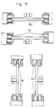
Wie aus Figur 13 zu ersehen ist, hat die eine Elektrode 130 der Sensorstruktur die Gestalt eines Biegebalkens mit kammförmigen Enden, wobei bei symmetrischem Aufbau der Biegebalken nur in seinem mittleren Bereich 130a mit dem Substrat 80 fest verbunden ist, während die übrigen Bereiche das Substrat nicht berühren und daher in der Substratebene frei auslenkbar sind. Die Gegenelektrode 131 hingegen ist fest mit dem Substrat 80 verbunden. Die Kämme greifen hierbei assymmetrisch ineinander.As can be seen from FIG. 13, one
Die beschriebene Sensoranodnung mit einem symmetrischen Biegebalken hat den Vorteil, daß sehr geringe Translationsbeschleunigungen unabhängig von überlagerten Winkelbeschleunigungen gemessen werden können, wobei die Größe der Winkelbeschleunigung in gleicher Größenordnung wie die Linearbeschleunigung liegen kann. Durch die gleichzeitige Herstellung zweier solcher Beschleunigungssensoren in senkrechtem Winkel zueinander auf demselben Chip gemäß Figur 14 ist damit eine winkelbeschleunigungsfreie Messung der Linearbeschleunigung in zwei Raumrichtungen möglich ohne zusätzliche Justierung.The sensor arrangement described with a symmetrical bending beam has the advantage that very small translational accelerations can be measured independently of superimposed angular accelerations, the size of the angular acceleration can be of the same order of magnitude as the linear acceleration. By simultaneously producing two such acceleration sensors at a perpendicular angle to one another on the same chip according to FIG. 14, an angular acceleration-free measurement of the linear acceleration in two spatial directions is possible without additional adjustment.
Mit einer leicht modifizierten Ausführung gemäß Figur 15 ist darüber hinaus die gleichzeitige Messung von Linear- und Winkelbeschleunigungen möglich, indem zwei Sensoranordnungen parallel zueinander auf einem gemeinsamen Chip hergestellt werden. Die assymmetrische Lage der Kämme zueinander ist hierbei so getroffen, daß die Anordnung 150 nur auf Linearbeschleunigungen anspricht und gegenüber Winkelbeschleunigungen unempfindlich ist. Bei der Anordnung 151 ist es umgekehrt, d.h. Winkelbeschleunigungen werden angezeigt, während bei Linearbeschleunigungen die Kapazitätsänderungen auf der linken und der rechten Seite des Biegebalkens sich kompensieren, also zu keiner Anzeige führen.With a slightly modified embodiment according to FIG. 15, the simultaneous measurement of linear and angular accelerations is also possible by producing two sensor arrangements parallel to one another on a common chip. The asymmetrical position of the combs with respect to one another is such that the
Die Sensorstrukturen können nicht nur, wie vorstehend beschrieben, auf der selben Seite wie die Schaltkreise, sondern auch auf der anderen Seite des Substrats aufgebaut werden. Bei komplexen Anordnungen können auch beide Seiten des Substrats mit Sensoranordnungen versehen werden. Auch in diesen Fällen wird die räumlich unmittelbar benachbarte Fertigung der Sensorstrukturen und der jeweils zugehörigen mit diesen gekoppelten Mikro-Schaltkreise zur integrierten Signalverarbeitung realisiert.The sensor structures can be constructed not only on the same side as the circuits, as described above, but also on the other side of the substrate. In the case of complex arrangements, both sides of the substrate can also be provided with sensor arrangements. In these cases, too, the spatially immediately adjacent manufacture of the sensor structures and the associated microcircuits coupled to them for integrated signal processing are realized.
Das Resistmaterial kann vor oder nach dem Zerteilen des Substrats entfernt werden. Das Entfernen nach dem Zerteilen hat den Vorteil, daß die empfindlichen Sensorstrukturen im Resistmaterial eingebettet und damit geschützt sind und das Zersägen erleichtert wird.The resist material can be removed before or after dicing the substrate. Removal after cutting has the advantage that the sensitive sensor structures are embedded in the resist material and thus protected, and sawing is made easier.
Claims (5)
Priority Applications (1)
| Application Number | Priority Date | Filing Date | Title |
|---|---|---|---|
| AT88907108T ATE76199T1 (en) | 1987-08-14 | 1988-08-08 | PROCESS FOR MANUFACTURING MICROSENSORS WITH INTEGRATED SIGNAL PROCESSING. |
Applications Claiming Priority (2)
| Application Number | Priority Date | Filing Date | Title |
|---|---|---|---|
| DE3727142 | 1987-08-14 | ||
| DE3727142A DE3727142C2 (en) | 1987-08-14 | 1987-08-14 | Process for the production of microsensors with integrated signal processing |
Publications (2)
| Publication Number | Publication Date |
|---|---|
| EP0371069A1 EP0371069A1 (en) | 1990-06-06 |
| EP0371069B1 true EP0371069B1 (en) | 1992-05-13 |
Family
ID=6333768
Family Applications (1)
| Application Number | Title | Priority Date | Filing Date |
|---|---|---|---|
| EP88907108A Expired - Lifetime EP0371069B1 (en) | 1987-08-14 | 1988-08-08 | Process for manufacturing microsensors with integrated signal processing |
Country Status (5)
| Country | Link |
|---|---|
| US (1) | US5194402A (en) |
| EP (1) | EP0371069B1 (en) |
| JP (1) | JPH0693513B2 (en) |
| DE (1) | DE3727142C2 (en) |
| WO (1) | WO1989001632A1 (en) |
Families Citing this family (39)
| Publication number | Priority date | Publication date | Assignee | Title |
|---|---|---|---|---|
| FI893874A7 (en) * | 1989-08-17 | 1991-02-18 | Vaisala Oy | KONTAKTFOERSEDD GIVARE MED SKIKTSTRUKTUR SAMT FOERFARANDE FOER UTFOERANDE AV KONTATERINGEN. |
| DE3939112A1 (en) * | 1989-11-25 | 1991-05-29 | Kernforschungsz Karlsruhe | DEVICE FOR POSITIONING OPTICAL FIBERS IN CONNECTING ELEMENTS |
| DE4001399C1 (en) * | 1990-01-19 | 1991-07-25 | Kernforschungszentrum Karlsruhe Gmbh, 7500 Karlsruhe, De | Metallic microstructures - formed on substrates, by putting poly:methyl methacrylate] between moulding tool and silicon substrate |
| DE4024275A1 (en) * | 1990-07-31 | 1992-02-06 | Kernforschungsz Karlsruhe | METHOD FOR THE PRODUCTION OF MICROSTRUCTURES WITH AREAS OF DIFFERENT STRUCTURAL HEIGHT |
| DE4027732A1 (en) * | 1990-09-01 | 1992-03-05 | Thiedig Ullrich | CAMERA CHIP FOR A CAMERA DETECTING AND EVALUATING DOTS |
| JPH04268725A (en) * | 1991-02-25 | 1992-09-24 | Canon Inc | Mechanical quantity detection sensor and its manufacturing method |
| DE4126107C2 (en) * | 1991-08-07 | 1993-12-16 | Bosch Gmbh Robert | Accelerometer and manufacturing method |
| US6903084B2 (en) | 1991-08-28 | 2005-06-07 | Sterix Limited | Steroid sulphatase inhibitors |
| DE4226430C2 (en) * | 1992-08-10 | 1996-02-22 | Karlsruhe Forschzent | Capacitive acceleration sensor |
| DE4304424C2 (en) * | 1993-02-13 | 1995-03-30 | Kernforschungsz Karlsruhe | Process for the production of microstructure elements on a substrate, which interact electromechanically, optically or electrically with integrated circuits |
| DE4310037C1 (en) * | 1993-03-27 | 1993-12-09 | Beermann Kg Martor Argentax | Knife with automatically retractable blade - has capacitive acceleration sensor in hollow handle coupled to electromagnetic lock for unlatching spring returned blade when translatory or angular acceleration exceeds threshold. |
| US5616514A (en) * | 1993-06-03 | 1997-04-01 | Robert Bosch Gmbh | Method of fabricating a micromechanical sensor |
| DE4406342C1 (en) * | 1994-02-26 | 1995-03-09 | Kernforschungsz Karlsruhe | Sensor and method for producing it |
| DE4411130A1 (en) * | 1994-03-30 | 1995-10-05 | Siemens Ag | Sensor unit with at least one acceleration sensor, e.g. B. for automotive airbag deployment, and methods for its manufacture |
| DE4418163B4 (en) * | 1994-05-25 | 2007-04-05 | Robert Bosch Gmbh | Process for the production of micromechanical structures |
| US5581035A (en) | 1994-08-29 | 1996-12-03 | The Charles Stark Draper Laboratory, Inc. | Micromechanical sensor with a guard band electrode |
| US5646348A (en) | 1994-08-29 | 1997-07-08 | The Charles Stark Draper Laboratory, Inc. | Micromechanical sensor with a guard band electrode and fabrication technique therefor |
| US5504026A (en) * | 1995-04-14 | 1996-04-02 | Analog Devices, Inc. | Methods for planarization and encapsulation of micromechanical devices in semiconductor processes |
| DE19522004A1 (en) * | 1995-06-21 | 1997-01-02 | Inst Mikrotechnik Mainz Gmbh | Method for producing partly movable micro structure(s) |
| JPH09135032A (en) * | 1995-11-08 | 1997-05-20 | Mitsubishi Electric Corp | Hybrid integrated circuit device for acceleration detection |
| EP0822415B1 (en) * | 1996-07-31 | 2003-03-26 | STMicroelectronics S.r.l. | Semiconductor integrated capacitive acceleration sensor and relative fabrication method |
| DE19641531A1 (en) * | 1996-10-09 | 1998-04-16 | Bosch Gmbh Robert | Micromechanical component and a method for its production |
| US5874356A (en) * | 1997-02-28 | 1999-02-23 | Taiwan Semiconductor Manufacturing Co. Ltd. | Method for forming zig-zag bordered openings in semiconductor structures |
| JP3187754B2 (en) * | 1997-09-26 | 2001-07-11 | 富士電機株式会社 | Semiconductor sensor and method of manufacturing the same |
| DE19732250A1 (en) * | 1997-07-26 | 1999-01-28 | Bosch Gmbh Robert | Process for the production of metallic microstructures |
| KR100276387B1 (en) * | 1998-01-08 | 2000-12-15 | 윤종용 | A method for forming self-aligned contact of semiconductor device |
| EP0969512B1 (en) * | 1998-06-30 | 2009-05-13 | Asulab S.A. | Inductive sensor |
| DE59914876D1 (en) * | 1998-07-08 | 2008-11-06 | Infineon Technologies Ag | METHOD FOR PRODUCING AN INTEGRATED CIRCUIT ARRANGEMENT COMPRISING A CAVITY IN A MATERIAL LAYER, AND AN INTEGRATED CIRCUIT ARRANGED BY THE PROCESS |
| DE19832905C2 (en) * | 1998-07-22 | 2000-06-29 | Karlsruhe Forschzent | Capacitive acceleration sensor |
| US6278186B1 (en) | 1998-08-26 | 2001-08-21 | Intersil Corporation | Parasitic current barriers |
| JP2001005942A (en) * | 1999-06-24 | 2001-01-12 | Shinko Electric Ind Co Ltd | IC card, method of manufacturing the same, semiconductor device with antenna and method of manufacturing the same |
| US6262463B1 (en) * | 1999-07-08 | 2001-07-17 | Integrated Micromachines, Inc. | Micromachined acceleration activated mechanical switch and electromagnetic sensor |
| DE19955975A1 (en) * | 1999-11-19 | 2001-05-23 | Inst Mikrotechnik Mainz Gmbh | Lithographic process for the production of micro components |
| US6720635B1 (en) | 1999-12-17 | 2004-04-13 | Motorola, Inc. | Electronic component |
| US7335650B2 (en) * | 2000-01-14 | 2008-02-26 | Sterix Limited | Composition |
| KR100543291B1 (en) * | 2001-12-03 | 2006-01-20 | 주식회사 포스코 | Backup roll pin for backup roll |
| DE10161492C5 (en) * | 2001-12-14 | 2007-05-10 | Micromotion Gmbh | Method for producing and storing microcomponents, magazine and assembly method for microcomponents |
| US20050180845A1 (en) * | 2002-04-04 | 2005-08-18 | Vreeke Mark S. | Miniature/micro-scale power generation system |
| DE10247487A1 (en) * | 2002-10-11 | 2004-05-06 | Infineon Technologies Ag | Membrane and process for its manufacture |
Family Cites Families (8)
| Publication number | Priority date | Publication date | Assignee | Title |
|---|---|---|---|---|
| DE2028819C3 (en) * | 1970-06-11 | 1980-05-29 | Siemens Ag, 1000 Berlin Und 8000 Muenchen | Process for producing a metal contact with a contact height> 10 µm |
| US4078963A (en) * | 1973-12-10 | 1978-03-14 | U.S. Philips Corporation | Method of manufacturing a semiconductor device, having a pattern of conductors on a supporting body |
| US3993515A (en) * | 1975-03-31 | 1976-11-23 | Rca Corporation | Method of forming raised electrical contacts on a semiconductor device |
| US4436766A (en) * | 1981-05-15 | 1984-03-13 | The United States Of America As Represented By The Secretary Of The Navy | Plated bridge step-over connection for monolithic devices and method for making thereof |
| DE3204425A1 (en) * | 1982-02-09 | 1983-08-25 | Siemens AG, 1000 Berlin und 8000 München | METHOD FOR PRODUCING SUPPORTING METAL GRID STRUCTURES |
| DE3328899C2 (en) * | 1983-08-10 | 1985-07-11 | Nukem Gmbh, 6450 Hanau | Photovoltaic cell |
| JPH02277242A (en) * | 1989-04-18 | 1990-11-13 | Nec Corp | Manufacture of semiconductor device |
| US4943539A (en) * | 1989-05-09 | 1990-07-24 | Motorola, Inc. | Process for making a multilayer metallization structure |
-
1987
- 1987-08-14 DE DE3727142A patent/DE3727142C2/en not_active Expired - Fee Related
-
1988
- 1988-08-08 US US07/340,175 patent/US5194402A/en not_active Expired - Lifetime
- 1988-08-08 JP JP63506552A patent/JPH0693513B2/en not_active Expired - Lifetime
- 1988-08-08 WO PCT/DE1988/000488 patent/WO1989001632A1/en not_active Ceased
- 1988-08-08 EP EP88907108A patent/EP0371069B1/en not_active Expired - Lifetime
Non-Patent Citations (2)
| Title |
|---|
| Technische Rundschau, vol. 78, No. 35, August 1986, (Bern, CH), H. Benninghof: "Mikrostrukturtechnologie für innovative Produkte", pages 32-37 see pages 34-35, chapter: "Mikrofertigung nach dem LIGA-Verfahren"; pages 35-36, chapter: "Mikromechanik und siliziumtechnologie" * |
| Technische Rundschau, vol. 79, no. 13, 27 March 1987, (Bern, CH), E.-K. Aschmoneit: "LIGA: Mikrostrukturen, lithographisch hergestellt", pages 54-57 * |
Also Published As
| Publication number | Publication date |
|---|---|
| DE3727142A1 (en) | 1989-02-23 |
| JPH0693513B2 (en) | 1994-11-16 |
| WO1989001632A1 (en) | 1989-02-23 |
| JPH02500475A (en) | 1990-02-15 |
| DE3727142C2 (en) | 1994-02-24 |
| US5194402A (en) | 1993-03-16 |
| EP0371069A1 (en) | 1990-06-06 |
Similar Documents
| Publication | Publication Date | Title |
|---|---|---|
| EP0371069B1 (en) | Process for manufacturing microsensors with integrated signal processing | |
| DE19619921B4 (en) | Method for producing a semiconductor device with functional element and protective cap | |
| EP0002185B1 (en) | Process for interconnecting two crossed conducting metal lines deposited on a substrate | |
| DE68929150T2 (en) | Method of manufacturing a semiconductor device | |
| EP0721587B1 (en) | Micromechanical device and process for producing the same | |
| DE69305955T2 (en) | ACCELERATION SENSOR AND ITS PRODUCTION | |
| DE3335772C2 (en) | Transducer and method for producing a transducer that operates on a piezoresistance basis | |
| DE3343035C2 (en) | Method for producing a magnetic sensor with at least two elements with magnetic resistance change | |
| DE3900654C2 (en) | Pressure sensor arrangement and method for its production | |
| EP0494143B1 (en) | Device for measuring mechanical forces and dynamic effects | |
| DE19719601A1 (en) | Acceleration sensor with spring-mounted seismic mass | |
| DE102012100007A1 (en) | Semiconductor devices with insulating substrates and methods of forming the same | |
| WO2000031796A1 (en) | Method for producing an integrated circuit processed on both sides | |
| DE102005005320A1 (en) | Magnetic sensor device and its manufacturing method | |
| DE102008007170A1 (en) | Acceleration sensor and manufacturing method of the same | |
| DE2315710B2 (en) | Method for manufacturing a semiconductor device | |
| DE69514343T2 (en) | SEMICONDUCTOR DEVICE WITH A MICRO COMPONENT THAT HAS A RIGID AND A MOVING ELECTRODE | |
| EP0167732B1 (en) | Method for producing a basic material for a hybrid circuit | |
| EP0342274B1 (en) | Arrangement for reducing the piezo effects in a semiconductor material that contains at least one piezo effect-sensitive electric device, and method of making the same | |
| DE19819456B4 (en) | Method for producing a micromechanical component | |
| EP1522095B1 (en) | Method for producing a component having submerged connecting areas | |
| DE60025214T2 (en) | Micro cover housing on disc level | |
| DE10019408C2 (en) | Field effect transistor, in particular for use as a sensor element or acceleration sensor, and method for its production | |
| DE2458410A1 (en) | MANUFACTURING PROCESS FOR A POWER SEMI-CONDUCTOR WITH PRESS CONTACTS | |
| EP1238311B1 (en) | Flat coil and lithographic method for producing microcomponents |
Legal Events
| Date | Code | Title | Description |
|---|---|---|---|
| PUAI | Public reference made under article 153(3) epc to a published international application that has entered the european phase |
Free format text: ORIGINAL CODE: 0009012 |
|
| 17P | Request for examination filed |
Effective date: 19890519 |
|
| AK | Designated contracting states |
Kind code of ref document: A1 Designated state(s): AT BE CH DE FR GB IT LI LU NL SE |
|
| RBV | Designated contracting states (corrected) |
Designated state(s): AT CH FR GB IT LI NL SE |
|
| REG | Reference to a national code |
Ref country code: DE Ref legal event code: 8566 |
|
| 17Q | First examination report despatched |
Effective date: 19910926 |
|
| ITF | It: translation for a ep patent filed | ||
| GRAA | (expected) grant |
Free format text: ORIGINAL CODE: 0009210 |
|
| AK | Designated contracting states |
Kind code of ref document: B1 Designated state(s): AT CH FR GB IT LI NL SE |
|
| REF | Corresponds to: |
Ref document number: 76199 Country of ref document: AT Date of ref document: 19920515 Kind code of ref document: T |
|
| ET | Fr: translation filed | ||
| GBT | Gb: translation of ep patent filed (gb section 77(6)(a)/1977) | ||
| PLBE | No opposition filed within time limit |
Free format text: ORIGINAL CODE: 0009261 |
|
| STAA | Information on the status of an ep patent application or granted ep patent |
Free format text: STATUS: NO OPPOSITION FILED WITHIN TIME LIMIT |
|
| 26N | No opposition filed | ||
| EAL | Se: european patent in force in sweden |
Ref document number: 88907108.0 |
|
| PGFP | Annual fee paid to national office [announced via postgrant information from national office to epo] |
Ref country code: SE Payment date: 19970818 Year of fee payment: 10 |
|
| PGFP | Annual fee paid to national office [announced via postgrant information from national office to epo] |
Ref country code: AT Payment date: 19970826 Year of fee payment: 10 |
|
| PGFP | Annual fee paid to national office [announced via postgrant information from national office to epo] |
Ref country code: NL Payment date: 19970828 Year of fee payment: 10 |
|
| PGFP | Annual fee paid to national office [announced via postgrant information from national office to epo] |
Ref country code: FR Payment date: 19970829 Year of fee payment: 10 |
|
| PG25 | Lapsed in a contracting state [announced via postgrant information from national office to epo] |
Ref country code: AT Free format text: LAPSE BECAUSE OF NON-PAYMENT OF DUE FEES Effective date: 19980808 |
|
| PG25 | Lapsed in a contracting state [announced via postgrant information from national office to epo] |
Ref country code: SE Free format text: LAPSE BECAUSE OF NON-PAYMENT OF DUE FEES Effective date: 19980809 |
|
| PG25 | Lapsed in a contracting state [announced via postgrant information from national office to epo] |
Ref country code: NL Free format text: LAPSE BECAUSE OF NON-PAYMENT OF DUE FEES Effective date: 19990301 |
|
| PG25 | Lapsed in a contracting state [announced via postgrant information from national office to epo] |
Ref country code: FR Free format text: LAPSE BECAUSE OF NON-PAYMENT OF DUE FEES Effective date: 19990430 |
|
| EUG | Se: european patent has lapsed |
Ref document number: 88907108.0 |
|
| NLV4 | Nl: lapsed or anulled due to non-payment of the annual fee |
Effective date: 19990301 |
|
| REG | Reference to a national code |
Ref country code: FR Ref legal event code: ST |
|
| REG | Reference to a national code |
Ref country code: GB Ref legal event code: IF02 |
|
| PGFP | Annual fee paid to national office [announced via postgrant information from national office to epo] |
Ref country code: GB Payment date: 20050627 Year of fee payment: 18 |
|
| PGFP | Annual fee paid to national office [announced via postgrant information from national office to epo] |
Ref country code: CH Payment date: 20050722 Year of fee payment: 18 |
|
| PG25 | Lapsed in a contracting state [announced via postgrant information from national office to epo] |
Ref country code: IT Free format text: LAPSE BECAUSE OF NON-PAYMENT OF DUE FEES;WARNING: LAPSES OF ITALIAN PATENTS WITH EFFECTIVE DATE BEFORE 2007 MAY HAVE OCCURRED AT ANY TIME BEFORE 2007. THE CORRECT EFFECTIVE DATE MAY BE DIFFERENT FROM THE ONE RECORDED. Effective date: 20050808 |
|
| PG25 | Lapsed in a contracting state [announced via postgrant information from national office to epo] |
Ref country code: LI Free format text: LAPSE BECAUSE OF NON-PAYMENT OF DUE FEES Effective date: 20060831 Ref country code: CH Free format text: LAPSE BECAUSE OF NON-PAYMENT OF DUE FEES Effective date: 20060831 |
|
| REG | Reference to a national code |
Ref country code: CH Ref legal event code: PL |
|
| GBPC | Gb: european patent ceased through non-payment of renewal fee |
Effective date: 20060808 |
|
| PG25 | Lapsed in a contracting state [announced via postgrant information from national office to epo] |
Ref country code: GB Free format text: LAPSE BECAUSE OF NON-PAYMENT OF DUE FEES Effective date: 20060808 |