EP0002185B1 - Process for interconnecting two crossed conducting metal lines deposited on a substrate - Google Patents
Process for interconnecting two crossed conducting metal lines deposited on a substrate Download PDFInfo
- Publication number
- EP0002185B1 EP0002185B1 EP78101133A EP78101133A EP0002185B1 EP 0002185 B1 EP0002185 B1 EP 0002185B1 EP 78101133 A EP78101133 A EP 78101133A EP 78101133 A EP78101133 A EP 78101133A EP 0002185 B1 EP0002185 B1 EP 0002185B1
- Authority
- EP
- European Patent Office
- Prior art keywords
- layer
- metal layer
- lines
- level
- metallization
- Prior art date
- Legal status (The legal status is an assumption and is not a legal conclusion. Google has not performed a legal analysis and makes no representation as to the accuracy of the status listed.)
- Expired
Links
Images


Classifications
-
- H—ELECTRICITY
- H01—ELECTRIC ELEMENTS
- H01L—SEMICONDUCTOR DEVICES NOT COVERED BY CLASS H10
- H01L21/00—Processes or apparatus adapted for the manufacture or treatment of semiconductor or solid state devices or of parts thereof
- H01L21/70—Manufacture or treatment of devices consisting of a plurality of solid state components formed in or on a common substrate or of parts thereof; Manufacture of integrated circuit devices or of parts thereof
- H01L21/71—Manufacture of specific parts of devices defined in group H01L21/70
- H01L21/768—Applying interconnections to be used for carrying current between separate components within a device comprising conductors and dielectrics
- H01L21/76838—Applying interconnections to be used for carrying current between separate components within a device comprising conductors and dielectrics characterised by the formation and the after-treatment of the conductors
- H01L21/76841—Barrier, adhesion or liner layers
- H01L21/7685—Barrier, adhesion or liner layers the layer covering a conductive structure
-
- H—ELECTRICITY
- H01—ELECTRIC ELEMENTS
- H01L—SEMICONDUCTOR DEVICES NOT COVERED BY CLASS H10
- H01L21/00—Processes or apparatus adapted for the manufacture or treatment of semiconductor or solid state devices or of parts thereof
- H01L21/02—Manufacture or treatment of semiconductor devices or of parts thereof
- H01L21/04—Manufacture or treatment of semiconductor devices or of parts thereof the devices having at least one potential-jump barrier or surface barrier, e.g. PN junction, depletion layer or carrier concentration layer
- H01L21/18—Manufacture or treatment of semiconductor devices or of parts thereof the devices having at least one potential-jump barrier or surface barrier, e.g. PN junction, depletion layer or carrier concentration layer the devices having semiconductor bodies comprising elements of Group IV of the Periodic System or AIIIBV compounds with or without impurities, e.g. doping materials
- H01L21/30—Treatment of semiconductor bodies using processes or apparatus not provided for in groups H01L21/20 - H01L21/26
- H01L21/31—Treatment of semiconductor bodies using processes or apparatus not provided for in groups H01L21/20 - H01L21/26 to form insulating layers thereon, e.g. for masking or by using photolithographic techniques; After treatment of these layers; Selection of materials for these layers
- H01L21/3205—Deposition of non-insulating-, e.g. conductive- or resistive-, layers on insulating layers; After-treatment of these layers
- H01L21/321—After treatment
- H01L21/3213—Physical or chemical etching of the layers, e.g. to produce a patterned layer from a pre-deposited extensive layer
- H01L21/32133—Physical or chemical etching of the layers, e.g. to produce a patterned layer from a pre-deposited extensive layer by chemical means only
- H01L21/32134—Physical or chemical etching of the layers, e.g. to produce a patterned layer from a pre-deposited extensive layer by chemical means only by liquid etching only
-
- H—ELECTRICITY
- H01—ELECTRIC ELEMENTS
- H01L—SEMICONDUCTOR DEVICES NOT COVERED BY CLASS H10
- H01L21/00—Processes or apparatus adapted for the manufacture or treatment of semiconductor or solid state devices or of parts thereof
- H01L21/02—Manufacture or treatment of semiconductor devices or of parts thereof
- H01L21/04—Manufacture or treatment of semiconductor devices or of parts thereof the devices having at least one potential-jump barrier or surface barrier, e.g. PN junction, depletion layer or carrier concentration layer
- H01L21/18—Manufacture or treatment of semiconductor devices or of parts thereof the devices having at least one potential-jump barrier or surface barrier, e.g. PN junction, depletion layer or carrier concentration layer the devices having semiconductor bodies comprising elements of Group IV of the Periodic System or AIIIBV compounds with or without impurities, e.g. doping materials
- H01L21/30—Treatment of semiconductor bodies using processes or apparatus not provided for in groups H01L21/20 - H01L21/26
- H01L21/31—Treatment of semiconductor bodies using processes or apparatus not provided for in groups H01L21/20 - H01L21/26 to form insulating layers thereon, e.g. for masking or by using photolithographic techniques; After treatment of these layers; Selection of materials for these layers
- H01L21/3205—Deposition of non-insulating-, e.g. conductive- or resistive-, layers on insulating layers; After-treatment of these layers
- H01L21/321—After treatment
- H01L21/3213—Physical or chemical etching of the layers, e.g. to produce a patterned layer from a pre-deposited extensive layer
- H01L21/32133—Physical or chemical etching of the layers, e.g. to produce a patterned layer from a pre-deposited extensive layer by chemical means only
- H01L21/32135—Physical or chemical etching of the layers, e.g. to produce a patterned layer from a pre-deposited extensive layer by chemical means only by vapour etching only
- H01L21/32136—Physical or chemical etching of the layers, e.g. to produce a patterned layer from a pre-deposited extensive layer by chemical means only by vapour etching only using plasmas
-
- H—ELECTRICITY
- H01—ELECTRIC ELEMENTS
- H01L—SEMICONDUCTOR DEVICES NOT COVERED BY CLASS H10
- H01L21/00—Processes or apparatus adapted for the manufacture or treatment of semiconductor or solid state devices or of parts thereof
- H01L21/70—Manufacture or treatment of devices consisting of a plurality of solid state components formed in or on a common substrate or of parts thereof; Manufacture of integrated circuit devices or of parts thereof
- H01L21/71—Manufacture of specific parts of devices defined in group H01L21/70
- H01L21/768—Applying interconnections to be used for carrying current between separate components within a device comprising conductors and dielectrics
- H01L21/76838—Applying interconnections to be used for carrying current between separate components within a device comprising conductors and dielectrics characterised by the formation and the after-treatment of the conductors
- H01L21/76885—By forming conductive members before deposition of protective insulating material, e.g. pillars, studs
-
- H—ELECTRICITY
- H01—ELECTRIC ELEMENTS
- H01L—SEMICONDUCTOR DEVICES NOT COVERED BY CLASS H10
- H01L23/00—Details of semiconductor or other solid state devices
- H01L23/52—Arrangements for conducting electric current within the device in operation from one component to another, i.e. interconnections, e.g. wires, lead frames
- H01L23/522—Arrangements for conducting electric current within the device in operation from one component to another, i.e. interconnections, e.g. wires, lead frames including external interconnections consisting of a multilayer structure of conductive and insulating layers inseparably formed on the semiconductor body
- H01L23/5226—Via connections in a multilevel interconnection structure
-
- H—ELECTRICITY
- H01—ELECTRIC ELEMENTS
- H01L—SEMICONDUCTOR DEVICES NOT COVERED BY CLASS H10
- H01L2924/00—Indexing scheme for arrangements or methods for connecting or disconnecting semiconductor or solid-state bodies as covered by H01L24/00
- H01L2924/0001—Technical content checked by a classifier
- H01L2924/0002—Not covered by any one of groups H01L24/00, H01L24/00 and H01L2224/00
Definitions
- the invention relates to a method for producing a connection between two intersecting first and second conductor runs running on the surface of a substrate, in which a first metal layer is applied to the surface of the substrate covered with an insulating layer, and using this metal layer the a first level of first conductor tracks are generated, an insulating layer containing connection openings is applied to these conductor tracks and the second conductor tracks lying in a second level are formed on this insulating layer from a second metal layer filling the connection openings.
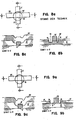
- FIGs. 8a to 8c show a connection point between a conductor run 6 'in a first metallization level and a conductor run 20' in a second metallization level. The connection was established through an opening in the insulating layer 12 separating the conductor tracks.
- a first metal layer 6 made of an alloy of aluminum, copper and silicon is first applied to a silicon substrate 2 or a silicon dioxide layer 4 covering it.
- the arrangement of the conductor tracks of the first metallization level obtained in this way is then covered with a quartz layer 12, which is applied, for example, by sputtering.
- This layer serves as an insulating layer between the conductor tracks of the first and the second metallization level.
- a connection opening is formed in the quartz layer 12 in a region of a conductor line 6 * of the first metallization level, in which an electrical connection between the first metallization level and the conductor lines of the second metallization level is provided.
- One of the conductor tracks 20 ′ of the second metallization level formed by photolithographic methods lies above the connection opening and establishes the desired electrical contact with the conductor track of the first metallization level.
- it is desirable that the conductor tracks of the second metallization level are so narrow that they do not completely cover the connection opening. This requirement would mean that the second conductor tracks are considerably wider than the connection opening in order to be able to compensate for alignment errors and other process tolerances.
- Either a wet chemical etching process with the aid of phosphoric acid or a reactive ion etching process with carbon tetrachloride is usually used to form the conductor tracks of the second metallization level.
- the problem with these manufacturing methods is that there is no reliable way to protect the conductor tracks 6 'of the first metallization level when etching the metal layer 20 of the second metallization level. Due to fluctuations in the thickness of the metal layer 20 of the second level of metallization within its tolerances and fluctuations in the orientation and width of the conductor tracks, it is necessary to set the parameters of the method in such a way that even a conductor tongue of the greatest thickness that is likely to occur is etched becomes. As a result, it cannot be avoided that, in the case of thin layers of the second metallization level, the conductor tracks 6 'of the first metallization level are overetched, as shown in FIGS. 8 to 26 and 26', for example.
- the conductor tracks 6 ' By overetching the conductor tracks 6 ', they have a smaller cross section at the crossing points and thus a higher current density. This contributes to excessive heat generation, electromigration and higher contact resistance due to higher current density. All of these things help reduce the reliability and quality of the resulting integrated circuit.
- an improvement in the connection to be established is sought by first planarizing the insulating layer covering the conductor tracks of the first metallization level in the region of the contact points. This is to prevent the side edges of the conductor tracks from being overetched during the production of the connection holes.
- the conductor tracks of the first metallization level are interrupted at the contact points in order to increase the insulating layer to avoid the contact points and thereby prevent overetching during the production of the connection holes.
- the interruption of the conductor tracks is later filled up again by the application of the metal layer of the second metallization level.
- the object of the invention is seen in specifying a method by means of which the conductor tracks of the first metallization level are prevented from being overetched when forming the conductor tracks of the second metallization level. In this way, especially in the case of structures with conductor tracks of the second metallization level that are narrow compared to the diameter of the connection holes, reliable connections are established.
- this object is achieved in that a further metal layer is applied to the first metal layer, that the first conductor tracks are formed from these two metal layers, the parts of the first produced from the further metal layer Conductor tracks serve as an etching barrier in the etching of the first metal layer and that the second metal layer is etched to form the second conductor tracks using an etching process in which the insulating layer separating the first and second conductor tracks is not significantly attacked and in which the parts formed from the further metal layer of the first conductor tracks serve as an etch stop for the parts of the first conductor tracks formed from the first metal layer.
- a chrome layer is advantageously applied to the metal layer of the first metallization level as an etching barrier.
- a quartz layer is applied as the insulating layer between the metallization levels, and the conductor tracks of the second metallization level are etched by reactive ion etching, preferably with a carbon tetrachloride-argon mixture at a temperature of at least 180 ° C.
- the etching of the conductor tracks of the second metallization level can also be carried out by wet chemical etching, preferably by means of a mixture of phosphoric acid and nitric acid. Silicon is added to the substances for forming the metallic layer of the first metallization level, while no silicon is added to the substances for forming the metallic layer of the second metallization level.
- the chrome layer applied as an etching barrier serves as a diffusion barrier.
- the advantage achieved by the invention essentially consists in the fact that with the help of the chrome layer serving as an etching barrier, overetching of the conductor tracks of the first metallization level is avoided, and better connections can thereby be made.
- the advantage is also achieved that the chromium layer serves as a diffusion barrier for the silicon which, in order to prevent the Si from diffusing out of the substrate, must be added to the metal in the first metallization level, but is undesirable in the second metallization level.
- FIGs. 1a to 7a a top view of an intersection of a conductor run of a first metallization level with a conductor run of a second metallization level is shown in different stages of the manufacturing process.
- the figures 1b to 7b represent the structures of FIGS. 1a to 7a corresponding cross sections along the line A-A '.
- non-overlapping arrangement of a through opening means in the case of a two-layer metallization structure that a conductor strip is used in the second metallization level, the width of which is less than or equal to the diameter of the opening which it has to penetrate in order to make contact with the first metallization level.
- Such a structure achieves a higher packing density of the metallic conductor tracks in the case of highly integrated, micro-miniaturized circuits.
- Figs. 1a and 1b show the first stage of the formation of an electrical connection between two metallization levels.
- a Si 2 layer 4 with a thickness of 0.2 to 0.5 ⁇ m is applied to the surface of a silicon substrate 2. Subsequently, in the first metallization plane, a 0.8 I Lm thick metal layer 6, for example, 95% aluminum, 4% copper and 1% silicon is evaporated.
- An essential component of the process described here is the vapor deposition of a 0.2 ⁇ m thick chrome layer 8, which serves as a barrier for the etching and protects the metal layer 6 during the subsequent process steps.
- a photoresist layer 10 is applied in the form of a pattern, by means of which the lines of the metal layer of the first level in layer 8 are determined.
- the next stage in the formation of the electrical connection between the two metallization. benen is in the Figs. 2a and 2b.
- a plasma etching chamber in which a plasma consisting of CF 4 + 10% O 2 is maintained at a pressure of approximately 1.33 mbar, a chrome strip 8 ', which has the shape of the conductor strip, is etched out of the chrome layer 8 .
- the layer 6 formed from an aluminum-copper-silicon alloy is etched to fix the course of the conductor track 6 'in the first metallization level. This is done by reactive ion etching using carbon tetrachloride + argon (40-60 mixture) at a temperature above 180 ° C, the workpiece being kept at a potential of - 200 V. Then the patterned photoresist layer 10 is removed in an ashing process using a high-frequency plasma of 20% O 2 and 80% N 2 at a pressure of 1.33 mbar.
- a 2.2 ⁇ m thick, flat quartz layer 12 is applied over and around the conductor strip of the first metallization level consisting of the strips 6 'and 8'. This is followed by the formation of a photoresist layer 14 which, according to the predetermined pattern, has an opening 16 at the location above the conductor 6 'at which the electrical through connection is to be made.
- a depression 18 is made in the quartz layer 12 and extends into the underlying layer (FIGS. 5a and 5b). This is done by plasma etching with a mixture of carbon tetrafluoride CF 4 and 8% oxygen at a pressure of approximately 1.33 mbar. The photoresist layer 14 is then removed.
- a layer 20 of an alloy of 95% aluminum and approximately 5% copper is applied to a thickness of 1.0 to 1.2 ⁇ m on the surface of the structured quartz layer 12 '.
- the layer 20 follows the surface of the quartz layer in the opening 18 and forms a recessed area 24.
- the metal layer 20 is the second layer of the metallization from which the upper conductor tracks of the double-layer structure are obtained.
- a photoresist layer 22 is applied in a pattern to its surface. This delimits a conductor line 20 'of the second detachment layer which intersects the conductor line 6' of the first metallization level in the opening 18.
- the method step 20 'of the second metallization level is etched by reactive ion etching with a carbon tetrachloride-argon mixture at a temperature of at least 180 ° C.
- the area 24 'of the conductor line 20' which passes through the opening 18 represents an electrical and mechanical contact with the conductor line 6 ', 8' of the first metallization level
- Aluminum-copper-silicon alloy existing conductor line 6 'of the first metallization level prevents over-etching of the conductor line 6' in the case of reactive ion etching, since the etching rate for chromium is only 1/6 of the etching rate for the Al-Cu-Si alloy.
- the etching rate for quartz is approximately 1/10 that of the Al-Cu-Si alloy.
- the conductor layer 6 ' is protected against attack during reactive ion etching by the chrome layer 8', and the exposed quartz layer 12 'is only negligibly affected.
- the conductor track 6 'thus formed does not suffer from overetched areas with reduced cross sections, which lead to a deterioration in the reliability and the electrical properties.
- the reactive ion etching of the conductor track 20 ' can be replaced by a wet etching process.
- a wet etching process For example, a mixture of phosphoric acid and nitric acid can be used to etch the aluminum-copper layer 20 '. This acid has a significantly reduced etching rate with chromium.
- the chromium protective layer 8 ' acts as an etching barrier, which protects the layer 6' underneath during the etching.
- the use of a wet etching process has the disadvantage that it tends to undercut the aluminum-copper-silicon metal of the conductor strip 6 'under the protective chrome layer 8', as a result of which the current-conducting cross section of the conductor strip is reduced. In cases where such a reduced cross-section can be tolerated in the first metallization level, the use of a wet etching process can be recommended.
- the els etching barrier for the conductor track 6 acting chrome layer 8 also has the advantage that it defines the width of the conductor track with greater reliability.
- the chrome layer forms a mask with a stable transverse dimension during the etching of the metallization in the first level.
- a photoresist mask is used to determine the shape of the conductor tracks in the first metallization level.
- the. Mask the tendency to melt away during reactive ion etching. This creates a bevelled course of the etched side edges of the conductor tracks. This problem is avoided by the mechanical stability of the chromium layer 8 'as a mask during the ion etching.
- the layer 8 acting as an etching barrier can also consist of other metals which are difficult to melt, such as Ti, Zr, V, Nb, Ta, W, Mo, Pt, Pd and Ni.
- the first metallization layer 6 is saturated with silicon in order to prevent silicon atoms from diffusing out of the substrate at the contact points with the metallization 6, as can occur with Schottky blocking diode contacts or with flat emitter contacts.
- the second metallization 20 which consists of an alloy not saturated with silicon, is brought into contact with the first metallization, a diffusion of the silicon atoms from the first metallization 6 into the second metallization 20 can be induced in the subsequent process steps at elevated temperature . This reduces the silicon concentration in the metal layer 6 and causes an undesired diffusion of silicon atoms from the substrate into the metal layer 26.
- FIGS. 9a nis 9c based on the representation of the prior art in FIGS. 8a to 8c again shown in a top view and in two mutually perpendicular cross sections along the lines A-A 'and B-B'.
Description
Die Erfindung bezieht sich auf ein Verfahren zum Herstellen einer Verbindung zwischen zwei sich kreuzenden, auf der Oberfläche eines Substrats verlaufenden ersten und zweiten Leiterzügen, bei welchem auf die mit einer Isolierschicht bedeckte Oberfläche des Substrats eine erste Metallschicht aufgebracht wird und unter Verwendung dieser Metallschicht die in einer ersten Ebene liegenden ersten Leiterzüge erzeugt werden, auf diese Leiterzüge eine Verbindungsöffnungen enthaltende Isolierschicht aufgebracht und auf dieser Isolierschicht aus einer zweiten, die Verbindungsöffnungen ausfüllenden Metallschicht die in einer zweiten Ebene liegenden zweiten Leiterzüge gebildet werden.The invention relates to a method for producing a connection between two intersecting first and second conductor runs running on the surface of a substrate, in which a first metal layer is applied to the surface of the substrate covered with an insulating layer, and using this metal layer the a first level of first conductor tracks are generated, an insulating layer containing connection openings is applied to these conductor tracks and the second conductor tracks lying in a second level are formed on this insulating layer from a second metal layer filling the connection openings.
Mit der Zunahme der Packungsdichte von integrierten Schaltungen wurde es notwendig, die Verbindungsleiterzüge zwischen den einzelnen Transistorstrukturen auf einem Halbleiterplättchen in mehr als einer Ebene anzuordnen. In den Fign. 8a bis 8c ist ein Verbindungspunkt zwischen einem Leiterzug 6' in einer ersten Metallisierungsebene und einem Leiterzug 20' in einer zweiten Metallisierungsebene dargestellt. Die Verbindung wurde durch eine Öffnung in der die Leiterzüge trennenden Isolierschicht 12 hergestellt.With the increase in the packing density of integrated circuits, it became necessary to arrange the connecting conductor tracks between the individual transistor structures on a semiconductor die in more than one plane. In Figs. 8a to 8c show a connection point between a conductor run 6 'in a first metallization level and a conductor run 20' in a second metallization level. The connection was established through an opening in the
Bei den üblichen Verfahren zur Herstellung dieser Struktur wird zunächst auf ein Siliciumsubstrat 2 oder eine dieses bedeckende Siliciumdioxid-Schicht 4 eine erste Metallschicht 6 aus einer Legierung aus Aluminium, Kupfer und Silicium aufgebracht. Die metallischen Leiterzüge 6' werden sodann durch photolithographische Verfahren abgegrenzt. Die so erhaltene Anordnung der Leiterzüge der ersten Metallisierungsebene wird sodann mit einer Quarzschicht 12, die beispielsweise durch Kathodenzerstäubung aufgebracht wird, bedeckt. Diese Schicht dient als Isolierschicht zwischen den Leiterzügen der ersten und der zweiten Metallisierungsebene. Dannach wird in einem Bereich eines Leiterzuges 6* der ersten Metallisierungsebene, in welchem eine elektrische Verbindung zwischen der ersten Metallisierungsebene und den Leiterzügen der zweiten Metallisierungsebene vorgesehen ist, in der Quarzschicht 12 eine Verbindungsöffnung gebildet. Diesem folgt die Aufbringung einer Metallschicht 20 in der zweiten Metallisierungsebene. Einer der durch photolithographische Verfahren gebildeten Leiterzüge 20' der zweiten Metallisierungsebene liegt über der Verbindungsöffnung und stellt den gewünschten elektrischen Kontakt mit dem Leiterzug der ersten Metallisierungsebene her. Um eine hohe Packungsdichte zu erreichen, ist es erwünscht, daß die Leiterzüge der zweiten Metallisierungsebene so schmal sind, daß sie die Verbindungsöffnung nicht ganz überdecken. Dieses Erfordernis würde bedeuten, daß die zweiten Leiterzüge wesentlich breiter sind als die Verbindungsöffnung, um Ausricht- - fehler und andere Verfahrenstoleranzen ausgleichen zu können. Zur Bildung der Leiterzüge der zweiten Metallisierungsebene wird üblicherweise entweder ein naßchemisches Ätzverfahren unter Zuhilfenahme von Phosphorsäure oder ein reaktives lonenätzverfahren mit Kohlenstofftetrachlorid verwendet.In the usual methods for producing this structure, a
Bei diesen Herstellungsverfahren besteht jedoch das Problem, daß es keinen zuverläßigen Weg gibt, um die Leiterzüge 6' der ersten Metallisierungsebene beim Ätzen der Metallschicht 20 der zweiten Metallisierungsebene zu schützen. Infolge von Schwankungen in der Dicke der Metallschicht 20 der zweiten Metallisierungsebene innerhalb ihrer Toleranzen und von Schwankungen in der Ausrichtung und der Breite der Leiterzüge zwingen dazu, die Parameter des Verfahrens so festzusetzen, daß auch noch ein Leiterzung der größten Dicke, die wahrscheinlichauftreten wird, geätzt wird. Dadurch läßt es sich nicht vermeiden, daß bei dünnen Schichten der zweiten Metallisierungsebene die Leiterzüge 6' der ersten Metallisierungsebene überätzt werden, dargestellt in Fig..-8 beispielsweise bei 26 und 26'. Durch das Überätzen der Leiterzüge 6' erhalten diese an den Kreuzungspunkten einen geringeren Querschnitt und damit eine höhere Stromdichte. Hieraus entsteht ein Beitrag zu übermäßiger Wärmeerzeugung, Elektromigration und höherem Kontaktwiderstand infolge höherer Stromdichte. Alle diese Dinge tragen dazu bei, die Zuverlässigkeit und die Qualität der resultierenden integrierten Schaltung herabzusetzen.However, the problem with these manufacturing methods is that there is no reliable way to protect the conductor tracks 6 'of the first metallization level when etching the
Bei einem bekannten Verfahren dieser Art, daß in der DOS 24 30 692 beschrieben ist, wird eine Verbesserung der herzustellenden Verbindung dadurch angestrebt, daß zunächst die Leiterzüge der ersten Metallisierungsebene bedeckende Isolierschicht im Bereich der Kontaktstellen planarisiert wird. Dadurch soll ein Überätzen der Seitenkanten der Leiterzüge bei der Herstellung der Verbindunglöcher verhindert werden.In a known method of this type, which is described in DOS 24 30 692, an improvement in the connection to be established is sought by first planarizing the insulating layer covering the conductor tracks of the first metallization level in the region of the contact points. This is to prevent the side edges of the conductor tracks from being overetched during the production of the connection holes.
Bei einem anderen bekannten Verfahren dieser Art, das im IBM Technical Disclosure Bulletin, Vol. 19, Nr. 11, April 1977, Seiten 4152, 4153 beschrieben ist, werden die Leiterzüge der ersten Metallisierungsebene an den Kontaktstellen unterbrochen, um eine Erhöhung der Isolierschicht an den Kontaktstellen zu vermeiden und dadurch ein Überätzen bei der Herstellung der Verbindungslöcher zu unterbinden. Die Unterbrechung der Leiterzüge wird später durch das Aufbringen der Metallschicht der zweiten Metallisierungsebene wieder aufgefüllt.In another known method of this type, which is described in the IBM Technical Disclosure Bulletin, Vol. 19, No. 11, April 1977, pages 4152, 4153, the conductor tracks of the first metallization level are interrupted at the contact points in order to increase the insulating layer to avoid the contact points and thereby prevent overetching during the production of the connection holes. The interruption of the conductor tracks is later filled up again by the application of the metal layer of the second metallization level.
Demgegenüber wird die Aufgabe der Erfindung darin gesehen, ein Verfahren anzugeben, durch welches beim Bilden der Leiterzüge der zweiten Metallisierungsebene ein Überätzen der Leiterzüge der ersten Metallisierungsebene verhindert wird. Auf diese Weise sollen dadurch, insbesondere bei Strukturen mit gegenüber dem Durchmesser der Verbindungslöcher schmalen Leiterzügen der zweiten Metallisierungsebene, zuverlässige Verbindungen hergestellt werden.In contrast, the object of the invention is seen in specifying a method by means of which the conductor tracks of the first metallization level are prevented from being overetched when forming the conductor tracks of the second metallization level. In this way, especially in the case of structures with conductor tracks of the second metallization level that are narrow compared to the diameter of the connection holes, reliable connections are established.
Gemäß der Erfindung, wie sie in den Ansprüchen gekennzeichnet ist, wird diese Aufgabe dadurch gelöst, daß auf die erste Metallschicht eine weitere Metallschicht aufgebracht wird, daß aus diesen beiden Metallschichten die ersten Leiterzüge gebildet werden, wobei die aus der weiteren Metallschicht erzeugten Teile der ersten Leiterzüge beim Ätzen der ersten Metallschicht als Ätzsperre dienen und daß die zweite Metallschicht zur Bildung der zweiten Leiterzüge unter Verwendung eines Ätzverfahrens geätzt wird, bei dem die die ersten und zweiten Leiterzüge trennende Isolierschicht nicht wesentlich angegriffen wird und bei dem die aus der weiteren Metallschicht gebildeten Teile der ersten Leiterzüge als Ätzsperre für die aus der ersten Metallischicht gebildeten Teile der ersten Leiterzüge dienen.According to the invention, as characterized in the claims, this object is achieved in that a further metal layer is applied to the first metal layer, that the first conductor tracks are formed from these two metal layers, the parts of the first produced from the further metal layer Conductor tracks serve as an etching barrier in the etching of the first metal layer and that the second metal layer is etched to form the second conductor tracks using an etching process in which the insulating layer separating the first and second conductor tracks is not significantly attacked and in which the parts formed from the further metal layer of the first conductor tracks serve as an etch stop for the parts of the first conductor tracks formed from the first metal layer.
In vorteilhafter Weise wird auf die Metallschicht der ersten Metallisierungsebene als Ätzsperre eine Chromschicht aufgebracht. Als Isolierschicht zwischen den Metallisierungsebenen wird eine Quartzschicht aufgebracht, und das Ätzen der Leiterzüge der zweiten Metallisierungsebene erfolgt durch reaktives Ionenätzen, vorzugsweise mit einem Kohlenstofftetrachlorid-Argon-Gemisch bei einer Temperatur von mindestens 180°C.A chrome layer is advantageously applied to the metal layer of the first metallization level as an etching barrier. A quartz layer is applied as the insulating layer between the metallization levels, and the conductor tracks of the second metallization level are etched by reactive ion etching, preferably with a carbon tetrachloride-argon mixture at a temperature of at least 180 ° C.
Das Ätzen der Leiterzüge der zweiten Metallisierungsebene kann auch durch naßchemisches Ätzen, vorzugsweise mittels einer Mischung aus Phosphorsäure und Salpetersäure durchgeführt werden. Den Stoffen zur Bildung der metallischen-Schicht der ersten Metallisierungsebene wird Silicium beigegeben, während den Stoffen zur Bildung der metallischen Schicht der zweiten Metallisierungsebene kein Silicium beigegeben wird. Dabei dient die als Ätzschranke aufgebrachte Chromschicht als Diffusionssperre.The etching of the conductor tracks of the second metallization level can also be carried out by wet chemical etching, preferably by means of a mixture of phosphoric acid and nitric acid. Silicon is added to the substances for forming the metallic layer of the first metallization level, while no silicon is added to the substances for forming the metallic layer of the second metallization level. The chrome layer applied as an etching barrier serves as a diffusion barrier.
Der durch die Erfindung erreichte Vorteil besteht im wesentlichen darin, daß mit Hilfe der als Ätzschranke dienenden Chromschicht ein Überätzen der Leiterzüge der ersten Metallisierungsebene vermieden wird, und dadurch bessere Verbindungen hergestellt werden können. Gleichzeitig wird auch der Vorteil erreicht, daß die Chromschicht als Diffusionssperre für das Silicium dient, das, um ein Ausdiffundieren des Si aus dem Substrat zu verhindern, dem Metall der ersten Metallisierungsebene zugegeben werden muß, in der zweiten Metallisierungsebene dagegen unerwünscht ist.The advantage achieved by the invention essentially consists in the fact that with the help of the chrome layer serving as an etching barrier, overetching of the conductor tracks of the first metallization level is avoided, and better connections can thereby be made. At the same time, the advantage is also achieved that the chromium layer serves as a diffusion barrier for the silicon which, in order to prevent the Si from diffusing out of the substrate, must be added to the metal in the first metallization level, but is undesirable in the second metallization level.
Die Erfindung wird anhand eines durch die Zeichnungen erläuterten Ausführungsbeispieles beschrieben.The invention will be described with reference to an embodiment illustrated by the drawings.
Es zeigen :
- Fign. 1a bis 7a jeweils in Draufsicht, verschiedene Verfahrensstufen bei der Herstellung einer elektrischen Verbindung zwischen den Leiterzügen zweier Metallisierungsebenen,
- Fign. 1b bis 7b die den Fign. 1a bis 7a entsprechenden Querschnitte entlang der Linie A-A',
- Fign. 8a bis 8c eine nach bekanntem Verfahren hergestellte Struktur dieser Art, in Draufsicht und in Querschnitten entlang den Linien A-A' und B-B', und
- Fign. 9a bis 9c in Anlehnung an die Darstellung der Fig..B, eine nach den in den Fign. 1 bis 7 dargestellten Verfahren entstandene Struktur, in Draufsicht und in Querschnitten entlang den Linien A-N und B-B'.
- Fig. 1a to 7a each in plan view, different process stages in the production of an electrical connection between the conductor tracks of two metallization levels,
- Fig. 1b to 7b which the FIGS. 1a to 7a corresponding cross sections along the line A-A ',
- Fig. 8a to 8c show a structure of this type produced by a known method, in plan view and in cross sections along the lines AA 'and B-B', and
- Fig. 9a to 9c based on the illustration of FIG. B, one according to the in FIGS. 1 to 7 illustrated process structure, in plan view and in cross sections along the lines AN and B-B '.
In den Fign. 1a bis 7a ist in Draufsicht eine Kreuzungstelle eines Leiterzuges einer ersten Metallisierungsebene mit einem Leiterzug einer zweiten Metallisierungsebene in verschiedenen Stufen des Herstellungsverfahrens dargestellt. Die Fign. 1b bis 7b stellen die den Strukturen der Fign. 1a bis 7a entsprechenden Querschnitte entlang der Linie A-A' dar.In Figs. 1a to 7a a top view of an intersection of a conductor run of a first metallization level with a conductor run of a second metallization level is shown in different stages of the manufacturing process. The figures 1b to 7b represent the structures of FIGS. 1a to 7a corresponding cross sections along the line A-A '.
Die Bezeichnung « nicht überlappende Anordnung einer Durchgangsöffnung » bedeutet bei einer zweilagigen Metallisierungsstruktur, daß in der zweiten Metallisierungsebene ein Leiterzug benutzt wird, dessen Breite kleiner oder gleich dem Durchmesser der Öffnung ist, welche er durchdringen muß, um Kontakt mit der ersten Metallisierungsebene herzustellen. Durch eine solche Struktur wird eine höhere Packungsdichte der metallischen Leiterzüge bei hochintegrierten, mikrominiaturisierten Schaltungen erreicht.The term "non-overlapping arrangement of a through opening" means in the case of a two-layer metallization structure that a conductor strip is used in the second metallization level, the width of which is less than or equal to the diameter of the opening which it has to penetrate in order to make contact with the first metallization level. Such a structure achieves a higher packing density of the metallic conductor tracks in the case of highly integrated, micro-miniaturized circuits.
In den Fign. 1a und 1b ist die erste Stufe der Bildung einer elektrischen Verbindung zwischen zwei Metallisierungsebenen dargestellt. Auf der Oberfläche eines Siliciumsubstrats 2 ist eine Si- ®2-Schicht 4 mit einer Dicke von 0,2 bis 0,5 µm aufgebracht. Anschließend wird in der ersten Metallisierungsebene eine 0,8 ILm dicke Metallschicht 6, beispielsweise aus 95 % Aluminium, 4 % Kupfer und 1 % Silicium, aufgedampft.In Figs. 1a and 1b show the first stage of the formation of an electrical connection between two metallization levels. A Si 2 layer 4 with a thickness of 0.2 to 0.5 μm is applied to the surface of a
Einen wesentlichen Bestandteil des hier beschriebenen Verfahrens bildet das Aufdampfen einer 0,2 µm dicken Chromschicht 8, die als Schranke für das Ätzen dient und die Metallschicht 6 während der nachfolgenden Verfahrenschritte schützt.An essential component of the process described here is the vapor deposition of a 0.2 μm
Dannach wird eine Photolackschicht 10 in Form eines Musters aufgebracht, durch welche die Linienführung der Metallschicht der ersten Ebene in der Schicht 8 festgelegt wird. Die nächste Stufe bei der Bildung der elektrischen Verbindung zwischen den Beiden Metallisierungse- . benen ist in den Fign. 2a und 2b dargestellt. Dabei wird in einer Plasma-Ätzkammer, in welcher bei einem Druck von ungefähr 1,33 mbar ein aus CF4 + 10 % O2 bestehendes Plasma aufrechterhalten wird, aus der Chromschicht 8 ein Chromstreifen 8', der die Form des Leiterzuges besitzt, herausgeätzt.Then a
In der nächsten Stufe, die in den Fign. 3a und 3b dargestellt ist, wird die aus einer Aluminium-Kupfer-Silicium-Legierung gebildete Schicht 6 zur Festlegung des Verlaufs des Leiterzuges 6' in der ersten Metallisierungsebene geätzt. Dies geschieht durch reaktives lonenätzen unter Verwendung von Kohlenstofftetrachlorid + Argon (40-60 Mischung) bei einer über 180 °C liegenden Temperatur, wobei das Werkstück auf einem Potential von - 200 V gehalten wird. Dannach wird in einem Veraschungsverfahren unter Verwendung eines Hochfrequenzplasmas von 20 % O2 und 80 % N2 bei einem Druck von 1,33 mbar die gemusterte Photolackschicht 10 entfernt.In the next stage, which is shown in FIGS. 3a and 3b, the
Im nächsten Schritt, der in den Fign. 4a und 4b dargestellt ist, wird eine 2,2 µm dicke, ebene Quarzschicht 12 über dem aus den Streifen 6' und 8' bestehenden Leiterzug der ersten Metallisierungsebene und um diesen herum aufgebracht. Darauf folgt die Bildung einer Photolackschicht 14, die nach dem vorgegebenen Muster eine Öffnung 16 an der Stelle über dem Leiterzug 6' aufweist, an der die elektrische Durchgangsverbindung hergestellt werden soll.In the next step, which is shown in FIGS. 4a and 4b, a 2.2 μm thick,
Als nächstes wird in die Quarzschicht 12 eine bis in die darunterliegende Schicht durchgehende Vertiefung 18 eingebracht (Fign. 5a und 5b). Dies geschieht durch Plasmaätzen mit einer Mischung aus Kohlenstofftetrafluorid CF4 und 8% Sauerstoff bei einem Druck von ungefähr, 1,33 mbar. Dannach wird die Photolackschicht 14 entfernt.Next, a
In der nächsten, in den Fign. 6a und 6b dargestellten Stufe wird eine Schicht 20 aus einer Legierung von 95 % Aluminium und ungefähr 5 % Kupfer bis zu einer Dicke von 1,0 bis 1,2 µm auf der Oberfläche der strukturierten Quarzschicht 12' aufgebracht. Die Schicht 20 folgt dabei der Oberfläche der Quarzschicht in der Öffnung 18 und bildet einen vertieften Bereich 24. Die Metallschicht 20 ist die zweite Lage der Metallisierung, aus der die oberen Leiterzüge der doppellagigen Struktur gewonnen werden. Auf ihrer Oberfläche wird eine Photolackschicht 22 in einem Muster aufgebracht. Dadurch wird ein Leiterzug 20' der zweiten detallisierungslage abgegrenzt, der den Leiterzug 6' der ersten Metallisierungsebene in der Öffnung 18 schneidet.In the next one, in Figs. 6a and 6b, a
Im nächsten, in den Fign. 7a und 7b dargestellten Verfahrensschritt wird der Leiterzug 20' der zweiten Metallisierungsebene durch reaktives lonenätzen mit einem Kohlenstofftetrachlorid-Argon-Gemisch bei einer Temperatur von mindestens 180 °C geätzt. Der Bereich 24' des Leiterzuges 20', der durch die Öffnung 18 hindurchgeht, stellt einen elektrischen und mechanischen Kontakt mit dem Leiterzug 6', 8' der ersten Metallisierungsebene dar. Unter der abdeckenden Wirkung der als Ätzsperre dienenden Chromschicht 8' über dem aus einer Aluminium-Kupfer-Silicium-Legierung bestehenden Leiterzug 6' der ersten Metallisierungsebene wird ein Überätzen des Leiterzuges 6' beim reaktiven lonenätzen vermieden, da die Ätzgeschwindigkeiten bei Chrom nur 1/6 der Ätzgeschwindigkeit bei der AI-Cu-Si-Legierung beträgt. Außerdem ist bei diesem Verfahren die Ätzgeschwindigkeit bei Quarz ungefähr 1/10 derjenigen bei der AI-Cu-Si-Legierung. Durch die Anprdnung der Chromschicht 8' wird der Leiterzug 6' vor einem Angriff beim reaktiven lonenätzen geschützt, und die exponierte Quarzschicht 12' wird nur vernächlässigbar engegriffen. Der gebildete Leiterzug 6' leidet damit nicht unter überäzten Bereichen mit verringerten Querschnitten, die zu einer Verschlechterung der Zuverlässigkeit und der elektrischen Eigenschaften führen.In the next, in Figs. 7a and 7b, the
In einer anderen Ausführungsform kann das reaktive lonenätzen des Leiterzuges 20' (Fign. 7a, 7b) durch ein Naßätzverfahren ersetzt werden. Beispielsweise kann zum Ätzen der Aluminium-Kupfer-Schicht 20' eine Mischung aus Phosphorsäure und Salpetersäure verwendet werden. Diese Säure hat eine wesentlich reduzierte Ätzgeschwindigkeit bei Chrom. Somit wirkt auch bei diesem Naßätzen die Chromschutzschicht 8' als Ätzsperre, die die darunterliegende Schicht 6' beim Ätzen schützt.In another embodiment, the reactive ion etching of the
Die Verwendung eines Naßätzverfahrens hat jedoch den Nachteil, daß dieses dazu neigt, das Aluminium-Kupfer-Silicium-Metall des Leiterzuges 6' unter der schützenden Chromschicht 8' zu unterschneiden, wodurch der- stromleitende Querschnitt des Leiterzuges reduziert wird. In den Fällen, in denen ein derartig reduzierter Querschnitt in der ersten Metallisierungsebene toleriert werden kann, kann jedoch die Verwendung eines Naßätzverfahrens empfohlen werden.However, the use of a wet etching process has the disadvantage that it tends to undercut the aluminum-copper-silicon metal of the conductor strip 6 'under the
Es wird darauf hingewiesen, daß die els Ätzsperre für den Leiterzug 6 wirkende Chromschicht 8' zusätzlich den Vorteil bietet, daß durch sie die Breite des Leiterzuges mit größerer Zuverlässigkeit definiert wird. Die Chromschicht bildet eine Maske mit einer stabilen Querdimension während des Ätzens der Metallisierung in der ersten Ebene. Bei bekannten Verfahren, bei denen eine Photolackmaske zur Feststellung der Gestalt der Leiterzüge in der ersten Metallisierungsebene verwendet wird, hat die. Maske die Tendenz, während des reaktiven Ionenätzens wegzuschmelzen. Dadurch entsteht ein abgeschrägter Verlauf der geätzten Seitenkanten der Leiterzüge. Dieses Problem wird durch die mechanische Stabilität der Chromschicht 8' als Maske bei der lonenätzung vermieden.It is pointed out that the els etching barrier for the
Die als Ätzsperre wirkende Schicht 8 kann außer Chrom auch aus anderen schwer schmelzbaren Metallen, wie Ti, Zr, V, Nb, Ta, W, Mo, Pt, Pd und Ni bestehen.In addition to chromium, the
Wie bereits erwähnt, ist die erste Metallisierungschicht 6 mit Silicium gesättigt, um zu verhindern, daß Siliciumatome an den Kontaktstellen mit der Metallisierung 6 aus dem Substrat herausdiffundieren, wie es bei Schottky-Sperrdiodenkontakten oder bei flächen Emitterkontakten vorkommen kann. Wenn nun die zweite Metallisierung 20, die aus einer nicht mit Silicium gesättigten Legierung besteht, mit der ersten Metallisierung in Kontakt gebracht wird, kann bei den nachfolgenden Verfahrensschritten bei erhöhter Temperatur eine Diffusion der Siliciumatome aus der ersten Metallisierung 6 in die zweite Metallisierung 20 induziert werden. Dadurch wird die Silicium-Konzentration in der Metallschicht 6 reduziert und eine unerwünschte Diffusion von Silicium-Atomen aus dem Substrat in die Metallschicht 26 verursacht. Durch das Aufbringen der Chromschicht 8 entsprechend dem beschriebenen Verfahren, wird eine Diffusionsschranke erzeugt, die die unerwünschte Diffusion von Silicium-Atomen aus der Metallisierung 6 verhindert:As already mentioned, the
Die nunmehr entstandene Struktur ist in den Fign. 9a nis 9c in Anlehnung an die Darstellung des Standes der Technik in den Fign. 8a bis 8c nochmals, in einer Draufsicht und in zwei zueinander senkrechten Querschnitten entlang den Linien A-A' und B-B' dargestellt.The structure that has now emerged is shown in FIGS. 9a nis 9c based on the representation of the prior art in FIGS. 8a to 8c again shown in a top view and in two mutually perpendicular cross sections along the lines A-A 'and B-B'.
Claims (6)
Applications Claiming Priority (2)
| Application Number | Priority Date | Filing Date | Title |
|---|---|---|---|
| US05/843,901 US4172004A (en) | 1977-10-20 | 1977-10-20 | Method for forming dense dry etched multi-level metallurgy with non-overlapped vias |
| US843901 | 1977-10-20 |
Publications (2)
| Publication Number | Publication Date |
|---|---|
| EP0002185A1 EP0002185A1 (en) | 1979-06-13 |
| EP0002185B1 true EP0002185B1 (en) | 1981-12-02 |
Family
ID=25291286
Family Applications (1)
| Application Number | Title | Priority Date | Filing Date |
|---|---|---|---|
| EP78101133A Expired EP0002185B1 (en) | 1977-10-20 | 1978-10-13 | Process for interconnecting two crossed conducting metal lines deposited on a substrate |
Country Status (4)
| Country | Link |
|---|---|
| US (1) | US4172004A (en) |
| EP (1) | EP0002185B1 (en) |
| JP (1) | JPS5462788A (en) |
| DE (1) | DE2861415D1 (en) |
Cited By (1)
| Publication number | Priority date | Publication date | Assignee | Title |
|---|---|---|---|---|
| US9918494B2 (en) | 2012-12-21 | 2018-03-20 | Philip Morris Products S.A. | Smoking article comprising an airflow directing element |
Families Citing this family (40)
| Publication number | Priority date | Publication date | Assignee | Title |
|---|---|---|---|---|
| US4229247A (en) * | 1978-12-26 | 1980-10-21 | International Business Machines Corporation | Glow discharge etching process for chromium |
| US4410622A (en) * | 1978-12-29 | 1983-10-18 | International Business Machines Corporation | Forming interconnections for multilevel interconnection metallurgy systems |
| JPS5595340A (en) * | 1979-01-10 | 1980-07-19 | Chiyou Lsi Gijutsu Kenkyu Kumiai | Preparation of semiconductor device |
| US4267012A (en) * | 1979-04-30 | 1981-05-12 | Fairchild Camera & Instrument Corp. | Process for patterning metal connections on a semiconductor structure by using a tungsten-titanium etch resistant layer |
| US4381215A (en) * | 1980-05-27 | 1983-04-26 | Burroughs Corporation | Method of fabricating a misaligned, composite electrical contact on a semiconductor substrate |
| JPS5710926A (en) * | 1980-06-25 | 1982-01-20 | Toshiba Corp | Manufacture of semiconductor device |
| US4336295A (en) * | 1980-12-22 | 1982-06-22 | Eastman Kodak Company | Method of fabricating a transparent metal oxide electrode structure on a solid-state electrooptical device |
| US4352716A (en) * | 1980-12-24 | 1982-10-05 | International Business Machines Corporation | Dry etching of copper patterns |
| US4703392A (en) * | 1982-07-06 | 1987-10-27 | General Electric Company | Microstrip line and method for fabrication |
| US4517225A (en) * | 1983-05-02 | 1985-05-14 | Signetics Corporation | Method for manufacturing an electrical interconnection by selective tungsten deposition |
| GB8316477D0 (en) * | 1983-06-16 | 1983-07-20 | Plessey Co Plc | Producing layered structure |
| US4451326A (en) * | 1983-09-07 | 1984-05-29 | Advanced Micro Devices, Inc. | Method for interconnecting metallic layers |
| JPS60136337A (en) * | 1983-12-22 | 1985-07-19 | モノリシツク・メモリ−ズ・インコ−ポレイテツド | Method of forming hillock suppressing layer in double layer process and its structure |
| US4580332A (en) * | 1984-03-26 | 1986-04-08 | Advanced Micro Devices, Inc. | Forming a conductive, protective layer for multilayer metallization |
| US4717449A (en) * | 1984-04-25 | 1988-01-05 | Honeywell Inc. | Dielectric barrier material |
| US4713682A (en) * | 1984-04-25 | 1987-12-15 | Honeywell Inc. | Dielectric barrier material |
| US4670091A (en) * | 1984-08-23 | 1987-06-02 | Fairchild Semiconductor Corporation | Process for forming vias on integrated circuits |
| US4892845A (en) * | 1984-08-31 | 1990-01-09 | Texas Instruments Incorporated | Method for forming contacts through a thick oxide layer on a semiconductive device |
| US4614021A (en) * | 1985-03-29 | 1986-09-30 | Motorola, Inc. | Pillar via process |
| US4789760A (en) * | 1985-04-30 | 1988-12-06 | Advanced Micro Devices, Inc. | Via in a planarized dielectric and process for producing same |
| JPS6276653A (en) * | 1985-09-30 | 1987-04-08 | Toshiba Corp | Semiconductor integrated circuit |
| US4840923A (en) * | 1986-04-30 | 1989-06-20 | International Business Machine Corporation | Simultaneous multiple level interconnection process |
| US4786962A (en) * | 1986-06-06 | 1988-11-22 | Hewlett-Packard Company | Process for fabricating multilevel metal integrated circuits and structures produced thereby |
| US5045150A (en) * | 1986-09-11 | 1991-09-03 | National Semiconductor Corp. | Plasma etching using a bilayer mask |
| JPS63114214A (en) * | 1986-09-11 | 1988-05-19 | フェアチャイルド セミコンダクタ コーポレーション | Plasma etching employing double-layer mask |
| US5007984A (en) * | 1987-09-28 | 1991-04-16 | Mitsubishi Denki Kabushiki Kaisha | Method for etching chromium film formed on substrate |
| GB2211348A (en) * | 1987-10-16 | 1989-06-28 | Philips Nv | A method of forming an interconnection between conductive levels |
| GB2214709A (en) * | 1988-01-20 | 1989-09-06 | Philips Nv | A method of enabling connection to a substructure forming part of an electronic device |
| US5084404A (en) * | 1988-03-31 | 1992-01-28 | Advanced Micro Devices | Gate array structure and process to allow optioning at second metal mask only |
| EP0403571A4 (en) * | 1988-03-31 | 1991-01-30 | Advanced Micro Devices, Inc. | Gate array structure and process to allow optioning at second metal mask only |
| US5023701A (en) * | 1988-03-31 | 1991-06-11 | Advanced Micro Devices, Inc. | Gate array structure and process to allow optioning at second metal mask only |
| JP2947818B2 (en) * | 1988-07-27 | 1999-09-13 | 株式会社日立製作所 | Method of filling in fine hole with metal and cvd device for executing same |
| JPH06160610A (en) * | 1989-12-26 | 1994-06-07 | Xerox Corp | Manufacture of discontinuous multiphase fresnel lens |
| US5627345A (en) * | 1991-10-24 | 1997-05-06 | Kawasaki Steel Corporation | Multilevel interconnect structure |
| US5256597A (en) * | 1992-09-04 | 1993-10-26 | International Business Machines Corporation | Self-aligned conducting etch stop for interconnect patterning |
| JP3457348B2 (en) * | 1993-01-15 | 2003-10-14 | 株式会社東芝 | Method for manufacturing semiconductor device |
| JPH07245343A (en) * | 1994-03-03 | 1995-09-19 | Toshiba Corp | Semiconductor device and its manufacture |
| US9761488B2 (en) * | 2015-07-17 | 2017-09-12 | Taiwan Semiconductor Manufacturing Company, Ltd. | Method for cleaning via of interconnect structure of semiconductor device structure |
| US20170117036A1 (en) | 2015-10-22 | 2017-04-27 | Sandisk Technologies Llc | Source line driver for three dimensional non-volatile memory |
| JP2018129481A (en) * | 2017-02-10 | 2018-08-16 | ルネサスエレクトロニクス株式会社 | Semiconductor device |
Family Cites Families (13)
| Publication number | Priority date | Publication date | Assignee | Title |
|---|---|---|---|---|
| US3881971A (en) * | 1972-11-29 | 1975-05-06 | Ibm | Method for fabricating aluminum interconnection metallurgy system for silicon devices |
| US3804738A (en) * | 1973-06-29 | 1974-04-16 | Ibm | Partial planarization of electrically insulative films by resputtering |
| US3868723A (en) * | 1973-06-29 | 1975-02-25 | Ibm | Integrated circuit structure accommodating via holes |
| US3880684A (en) * | 1973-08-03 | 1975-04-29 | Mitsubishi Electric Corp | Process for preparing semiconductor |
| US3900944A (en) * | 1973-12-19 | 1975-08-26 | Texas Instruments Inc | Method of contacting and connecting semiconductor devices in integrated circuits |
| US3856648A (en) * | 1973-12-19 | 1974-12-24 | Texas Instruments Inc | Method of forming contact and interconnect geometries for semiconductor devices and integrated circuits |
| US3969197A (en) * | 1974-02-08 | 1976-07-13 | Texas Instruments Incorporated | Method for fabricating a thin film capacitor |
| US3951709A (en) * | 1974-02-28 | 1976-04-20 | Lfe Corporation | Process and material for semiconductor photomask fabrication |
| US3930913A (en) * | 1974-07-18 | 1976-01-06 | Lfe Corporation | Process for manufacturing integrated circuits and metallic mesh screens |
| US3994793A (en) * | 1975-05-22 | 1976-11-30 | International Business Machines Corporation | Reactive ion etching of aluminum |
| FR2312114A1 (en) * | 1975-05-22 | 1976-12-17 | Ibm | Selective reactive etching of metal or semiconductor - using plasma contg. chlorine, bromine or iodine (cpds.) avoids undercutting |
| JPS51147286A (en) * | 1975-06-13 | 1976-12-17 | Nec Corp | Manufacturing process of semiconductor |
| US4076575A (en) * | 1976-06-30 | 1978-02-28 | International Business Machines Corporation | Integrated fabrication method of forming connectors through insulative layers |
-
1977
- 1977-10-20 US US05/843,901 patent/US4172004A/en not_active Expired - Lifetime
-
1978
- 1978-09-08 JP JP10988978A patent/JPS5462788A/en active Pending
- 1978-10-13 EP EP78101133A patent/EP0002185B1/en not_active Expired
- 1978-10-13 DE DE7878101133T patent/DE2861415D1/en not_active Expired
Cited By (1)
| Publication number | Priority date | Publication date | Assignee | Title |
|---|---|---|---|---|
| US9918494B2 (en) | 2012-12-21 | 2018-03-20 | Philip Morris Products S.A. | Smoking article comprising an airflow directing element |
Also Published As
| Publication number | Publication date |
|---|---|
| DE2861415D1 (en) | 1982-01-28 |
| US4172004A (en) | 1979-10-23 |
| EP0002185A1 (en) | 1979-06-13 |
| JPS5462788A (en) | 1979-05-21 |
Similar Documents
| Publication | Publication Date | Title |
|---|---|---|
| EP0002185B1 (en) | Process for interconnecting two crossed conducting metal lines deposited on a substrate | |
| DE2346565C2 (en) | Process for producing conductive connections between metallization layers lying one on top of the other in integrated semiconductor arrangements | |
| DE2729030C2 (en) | Method for producing a multilayer conductor pattern for monolithically integrated semiconductor circuits | |
| DE3339957C2 (en) | ||
| DE1965546C3 (en) | Semiconductor component | |
| DE10006964C2 (en) | Electronic component with a conductive connection between two conductive layers and method for producing an electronic component | |
| DE2945533C2 (en) | Method of manufacturing a wiring system | |
| DE2723944C2 (en) | Method for producing an arrangement from a structured layer and a pattern | |
| DE2637667A1 (en) | SEMI-CONDUCTOR ARRANGEMENT | |
| DE1903961B2 (en) | Semiconductor integrated circuit and process for its manufacture | |
| DE1614872A1 (en) | Multi-layered line system with ohmic contacts for integrated circuits | |
| DE3043289C2 (en) | ||
| DE2636971C2 (en) | Method for producing an insulating layer with a flat surface on an uneven surface of a substrate | |
| DE2740757C2 (en) | Semiconductor device and method for the production thereof | |
| EP0012220A1 (en) | Method of making a Schottky contact with a self aligned guard ring | |
| DE2510757A1 (en) | METHOD OF PRODUCING CARRIER SUBSTRATES FOR HIGHLY INTEGRATED SEMI-CONDUCTOR CIRCUIT PLATES AND SUBSTRATES PRODUCED BY THIS METHOD | |
| DE2351943A1 (en) | METHOD OF MANUFACTURING INTEGRATED CIRCUITS | |
| DE19614584A1 (en) | Air-bridge wiring appts. for semiconductor monolithic microwave integrated circuit | |
| DE2047799B2 (en) | Multi-layer conductor layers on a semiconductor substrate and method for producing such multi-layer conductor layers | |
| EP0105189B1 (en) | Method of producing metal electrodes of diversing thiekness for semiconductor devices, especially for power semiconductor devices such as thyristors | |
| EP0013728A1 (en) | Method for forming electrical connections between conducting layers in semiconductor structures | |
| DE2945385A1 (en) | Multilayer substrate for semiconductor chip esp. integrated circuit - with conducting zones sepd. by insulating layers | |
| EP0353719A2 (en) | Metal contact with overhanging edges and process of fabrication | |
| EP0760161A1 (en) | Process for applying a metallisation layer on an insulator and for piercing through-holes in said insulator by means of a single mask | |
| DE10104265A1 (en) | Method of manufacturing a semiconductor circuit arrangement |
Legal Events
| Date | Code | Title | Description |
|---|---|---|---|
| PUAI | Public reference made under article 153(3) epc to a published international application that has entered the european phase |
Free format text: ORIGINAL CODE: 0009012 |
|
| AK | Designated contracting states |
Designated state(s): DE FR GB |
|
| 17P | Request for examination filed | ||
| GRAA | (expected) grant |
Free format text: ORIGINAL CODE: 0009210 |
|
| AK | Designated contracting states |
Designated state(s): DE FR GB |
|
| REF | Corresponds to: |
Ref document number: 2861415 Country of ref document: DE Date of ref document: 19820128 |
|
| PGFP | Annual fee paid to national office [announced via postgrant information from national office to epo] |
Ref country code: DE Payment date: 19840926 Year of fee payment: 7 |
|
| PGFP | Annual fee paid to national office [announced via postgrant information from national office to epo] |
Ref country code: FR Payment date: 19840928 Year of fee payment: 7 |
|
| PG25 | Lapsed in a contracting state [announced via postgrant information from national office to epo] |
Ref country code: GB Effective date: 19891013 |
|
| GBPC | Gb: european patent ceased through non-payment of renewal fee | ||
| PG25 | Lapsed in a contracting state [announced via postgrant information from national office to epo] |
Ref country code: FR Effective date: 19900629 |
|
| PG25 | Lapsed in a contracting state [announced via postgrant information from national office to epo] |
Ref country code: DE Effective date: 19900703 |
|
| REG | Reference to a national code |
Ref country code: FR Ref legal event code: ST |
|
| PLBE | No opposition filed within time limit |
Free format text: ORIGINAL CODE: 0009261 |
|
| STAA | Information on the status of an ep patent application or granted ep patent |
Free format text: STATUS: NO OPPOSITION FILED WITHIN TIME LIMIT |