EP0361967B1 - Inductivité plane - Google Patents
Inductivité plane Download PDFInfo
- Publication number
- EP0361967B1 EP0361967B1 EP89309998A EP89309998A EP0361967B1 EP 0361967 B1 EP0361967 B1 EP 0361967B1 EP 89309998 A EP89309998 A EP 89309998A EP 89309998 A EP89309998 A EP 89309998A EP 0361967 B1 EP0361967 B1 EP 0361967B1
- Authority
- EP
- European Patent Office
- Prior art keywords
- planar inductor
- planar
- ferromagnetic
- layers
- stacked
- Prior art date
- Legal status (The legal status is an assumption and is not a legal conclusion. Google has not performed a legal analysis and makes no representation as to the accuracy of the status listed.)
- Expired - Lifetime
Links
- 230000005294 ferromagnetic effect Effects 0.000 claims description 90
- 229910000808 amorphous metal alloy Inorganic materials 0.000 claims description 34
- 239000011347 resin Substances 0.000 claims description 25
- 229920005989 resin Polymers 0.000 claims description 25
- 230000005415 magnetization Effects 0.000 claims description 18
- 230000035699 permeability Effects 0.000 claims description 17
- 230000008602 contraction Effects 0.000 claims description 10
- 229910045601 alloy Inorganic materials 0.000 claims description 8
- 239000000956 alloy Substances 0.000 claims description 8
- 229920000620 organic polymer Polymers 0.000 claims description 7
- 239000004734 Polyphenylene sulfide Substances 0.000 claims description 5
- 229920000069 polyphenylene sulfide Polymers 0.000 claims description 5
- 238000002425 crystallisation Methods 0.000 claims description 3
- 230000008025 crystallization Effects 0.000 claims description 3
- 229910052804 chromium Inorganic materials 0.000 claims description 2
- 229910052802 copper Inorganic materials 0.000 claims description 2
- 229910052735 hafnium Inorganic materials 0.000 claims description 2
- 229910052748 manganese Inorganic materials 0.000 claims description 2
- 229910052750 molybdenum Inorganic materials 0.000 claims description 2
- 229910052759 nickel Inorganic materials 0.000 claims description 2
- 229910052758 niobium Inorganic materials 0.000 claims description 2
- 229910052715 tantalum Inorganic materials 0.000 claims description 2
- 229910052719 titanium Inorganic materials 0.000 claims description 2
- 229910052721 tungsten Inorganic materials 0.000 claims description 2
- 229910052720 vanadium Inorganic materials 0.000 claims description 2
- 229910052726 zirconium Inorganic materials 0.000 claims description 2
- 230000000052 comparative effect Effects 0.000 description 24
- XEEYBQQBJWHFJM-UHFFFAOYSA-N Iron Chemical compound [Fe] XEEYBQQBJWHFJM-UHFFFAOYSA-N 0.000 description 17
- 239000000203 mixture Substances 0.000 description 15
- 230000005291 magnetic effect Effects 0.000 description 13
- 238000004519 manufacturing process Methods 0.000 description 12
- 229920001721 polyimide Polymers 0.000 description 10
- 239000004020 conductor Substances 0.000 description 9
- 230000000694 effects Effects 0.000 description 9
- 238000010438 heat treatment Methods 0.000 description 9
- 230000003247 decreasing effect Effects 0.000 description 8
- 238000000465 moulding Methods 0.000 description 8
- 239000011888 foil Substances 0.000 description 6
- 230000004907 flux Effects 0.000 description 5
- 229910052742 iron Inorganic materials 0.000 description 5
- 238000005096 rolling process Methods 0.000 description 4
- 229920006269 PPS film Polymers 0.000 description 3
- 239000000853 adhesive Substances 0.000 description 3
- 230000001070 adhesive effect Effects 0.000 description 3
- 229910000859 α-Fe Inorganic materials 0.000 description 3
- 230000005540 biological transmission Effects 0.000 description 2
- 239000007788 liquid Substances 0.000 description 2
- 229910001004 magnetic alloy Inorganic materials 0.000 description 2
- 238000000034 method Methods 0.000 description 2
- 230000015556 catabolic process Effects 0.000 description 1
- 238000006731 degradation reaction Methods 0.000 description 1
- 230000000593 degrading effect Effects 0.000 description 1
- 239000012299 nitrogen atmosphere Substances 0.000 description 1
- 229920006395 saturated elastomer Polymers 0.000 description 1
- 238000007789 sealing Methods 0.000 description 1
- 239000007787 solid Substances 0.000 description 1
- 230000037303 wrinkles Effects 0.000 description 1
Images


Classifications
-
- H—ELECTRICITY
- H01—ELECTRIC ELEMENTS
- H01F—MAGNETS; INDUCTANCES; TRANSFORMERS; SELECTION OF MATERIALS FOR THEIR MAGNETIC PROPERTIES
- H01F1/00—Magnets or magnetic bodies characterised by the magnetic materials therefor; Selection of materials for their magnetic properties
- H01F1/01—Magnets or magnetic bodies characterised by the magnetic materials therefor; Selection of materials for their magnetic properties of inorganic materials
- H01F1/03—Magnets or magnetic bodies characterised by the magnetic materials therefor; Selection of materials for their magnetic properties of inorganic materials characterised by their coercivity
- H01F1/12—Magnets or magnetic bodies characterised by the magnetic materials therefor; Selection of materials for their magnetic properties of inorganic materials characterised by their coercivity of soft-magnetic materials
- H01F1/14—Magnets or magnetic bodies characterised by the magnetic materials therefor; Selection of materials for their magnetic properties of inorganic materials characterised by their coercivity of soft-magnetic materials metals or alloys
- H01F1/147—Alloys characterised by their composition
- H01F1/153—Amorphous metallic alloys, e.g. glassy metals
- H01F1/15308—Amorphous metallic alloys, e.g. glassy metals based on Fe/Ni
-
- H—ELECTRICITY
- H01—ELECTRIC ELEMENTS
- H01F—MAGNETS; INDUCTANCES; TRANSFORMERS; SELECTION OF MATERIALS FOR THEIR MAGNETIC PROPERTIES
- H01F17/00—Fixed inductances of the signal type
- H01F17/0006—Printed inductances
- H01F17/0013—Printed inductances with stacked layers
-
- H—ELECTRICITY
- H01—ELECTRIC ELEMENTS
- H01F—MAGNETS; INDUCTANCES; TRANSFORMERS; SELECTION OF MATERIALS FOR THEIR MAGNETIC PROPERTIES
- H01F41/00—Apparatus or processes specially adapted for manufacturing or assembling magnets, inductances or transformers; Apparatus or processes specially adapted for manufacturing materials characterised by their magnetic properties
- H01F41/02—Apparatus or processes specially adapted for manufacturing or assembling magnets, inductances or transformers; Apparatus or processes specially adapted for manufacturing materials characterised by their magnetic properties for manufacturing cores, coils, or magnets
- H01F41/04—Apparatus or processes specially adapted for manufacturing or assembling magnets, inductances or transformers; Apparatus or processes specially adapted for manufacturing materials characterised by their magnetic properties for manufacturing cores, coils, or magnets for manufacturing coils
- H01F41/041—Printed circuit coils
- H01F41/046—Printed circuit coils structurally combined with ferromagnetic material
Definitions
- the present invention relates to a planar inductor applied to, e.g., a DC-to-DC converter.
- a conventional ferrite toroidal coil has been used as a choke coil on the output side of, e.g., a DC-to-DC converter.
- a planar inductor has been recently studied in order to achieve miniaturization of an apparatus.
- planar inductor with a structure having a spiral or meander planar coil, insulating layers stacked on both surfaces of the planar coil, and ferromagnetic layers stacked on the insulating layers is known.
- an amorphous alloy ribbon having a high permeability is used as a ferromagnetic layer.
- many amorphous alloys have a positive saturation magnetostriction.
- an amorphous alloy having a saturation magnetostriction is used as a normal toroidal magnetic core, complicated magnetic anisotropy occurs during a heat treatment for eliminating strain by an inverse magnetostrictive effect due to a flexural stress, and soft magnetic properties such as an effective permeability are degraded.
- a ribbon of the alloy is used in a planar state.
- planar inductor When the planar inductor is applied to a choke coil on the output side of, e.g., a DC-to-DC converter, a high-frequency current superposed with DC current is supplied to the planar inductor. Therefore, excellent DC superposition characteristics are required.
- the conventional planar inductor undesirably has poor DC superposition characteristics. This problem is caused because the magnetic characteristics of a ferromagnetic ribbon which has been conventionally used are inadequate. More specifically, in the planar inductor, a magnetic flux flows in a plane of a surface of the ferromagnetic ribbon. When the saturation magnetization of the ferromagnetic ribbon is low, however, even if a small DC magnetic field is superposed, a magnetic flux density is saturated. Although the ferromagnetic ribbon having a high permeability is used in order to obtain higher inductance, an inductance is reduced, thus degrading DC superposition characteristics.
- a ferromagnetic ribbon having a high permeability consisting of a Co-based amorphous alloy is known, and its saturation magnetization is higher than that of a ferrite.
- this saturation magnetization is insufficient to prevent a reduction in inductance, and the DC superposition characteristics are degraded.
- a Co-based amorphous alloy is used as a ferromagnetic ribbon. If the Co-based amorphous alloy ribbons are stacked, the DC superposition characteristics can be improved to some extent. However, if a large number of amorphous alloy ribbons are stacked, the thickness of the planar inductor is increased. Therefore, in consideration of an object to obtain a thin planar inductor, stacking a large number of amorphous alloy ribbons is not preferable.
- planar inductor is used in practice while being coated with a mold resin.
- the amorphous alloy ribbon has a positive saturation magnetostriction
- the surface of the planar inductor is coated with a liquid mold resin and the resin is hardened, a compressive stress is applied to the ferromagnetic ribbon upon contraction of the mold resin.
- An effective permeability is then decreased due to an inverse magnetostrictive effect, thus reducing an inductance.
- a planar inductor comprising a planar inductance element, an insulating layer stacked on each major surface of said inductance element, and a ferromagnetic layer stacked on the outer major surfaces of said insulating layers, wherein said ferromagnetic layers are divided into a plurality of portions as viewed in plan view of the layers and the thickness of said ferromagnetic layers is not more than 100 »m.
- the ferromagnetic layer which constitutes the planar inductor is two-dimensionally divided into a plurality of portions, a high-frequency loss can be decreased, and the efficiency of the DC-to-DC converter to which such a planar inductor is applied can be improved.
- a relaxation layer for contraction of a mold resin is preferably formed on a surface of the ferromagnetic layer, and the entire members are coated with a mold resin.
- a planar inductance element consists of, e.g., a spiral or meander coil.
- the spiral coil normally has a two-layered structure obtained by forming spiral conductors on the front and rear surfaces of an insulating layer, and connecting the conductors via a through hole. Note that if a terminal can be extracted without a problem, a spiral coil having only one layer of a spiral conductor can be used.
- the planar inductance element may be formed by stacking a plurality of spiral or meander coils. When these coils are stacked, an inductance is increased. In this case, a ferromagnetic layer is not preferably inserted between the coils, but only an insulating layer is inserted. This is because even if a ferromagnetic layer is inserted between the coils, it hardly contributes to an increase in inductance, but increases the thickness of the entire planar inductor to reduce an inductance per unit volume.
- One or a plurality of ferromagnetic layers may be stacked.
- a saturation magnetization Js (4 ⁇ M s ) of the ferromagnetic layer is set to be 1 T (10 kG) or more because if the saturation magnetization Js (4 ⁇ M s ) is less than 1 T (10 kG), DC superposition characteristics of the planar inductor are degraded.
- the thickness of the ferromagnetic layer is 100 »m or less for the following reasons. Assume that the planar inductor is applied to, e.g., a DC-to-DC converter, and it is used in a frequency band of 10 kHz or more. If the thickness of the ferromagnetic layer exceeds 100 »m, a generated magnetic flux does not enter inside the layer due to a surface effect. Thus, an inductance is not increased in proportion to an increase in thickness of the ferromagnetic layer, and an inductance per unit volume is reduced. Note that the thickness of the ferromagnetic layer is preferably 4 »m or more.
- the thickness of the ferromagnetic layer is less than 4 »m, a sectional area required for passing all the magnetic fluxes generated by supplying a current to a coil cannot be obtained. Therefore, leaked magnetic fluxes are increased, and the inductance is considerably reduced, thus reducing an inductance per unit volume.
- each ferromagnetic layer When a plurality of ferromagnetic layers are stacked, each ferromagnetic layer must satisfy the above-mentioned conditions.
- the ferromagnetic layer preferably has an effective permeability » 10k of 1 ⁇ 104 or more at a frequency of 10 kHz.
- an effective permeability » 10k of 1 ⁇ 104 or more at a frequency of 10 kHz When such a ferromagnetic layer is used, a planar inductor having high inductance can be obtained.
- an amorphous alloy ribbon represented by the following formula is used as a ferromagnetic layer: (Fe 1-a M a ) 100-b X b where M is at least one of Ti, V, Cr, Mn, Co, Ni, Zr, Nb, Mo, Hf, Ta, W, and Cu, and X is at least one of Si, B, P, C, Ge, and Al, and 0 ⁇ a ⁇ 0.15, and 12 ⁇ b ⁇ 30).
- the element M is a component which contributes to an improvement of a permeability in a high-frequency region and an increase in crystallization temperature. Even if a small amount of the component M is added, it exhibits the above-mentioned function. In practice, preferably, a ⁇ 0.01. When a > 0.15, it is not preferable in practice since a Curie temperature is extremely lowered.
- the element X is necessary to obtain an amorphous state.
- a combination of elements Si and B is preferable. Note that when b ⁇ 12 and b > 28, it is difficult to obtain an amorphous state, and hence preferably, 12 ⁇ b ⁇ 28. More preferably, 15 ⁇ b ⁇ 25.
- Si is preferably added in an amount of 2 to 13%, and preferably, 2 to 8%.
- amorphous alloys with the above composition have saturation magnetizations of 1 T (10kG) or more.
- an effective permeability of 1 ⁇ 104 or more can be obtained.
- a ferromagnetic layer having an extremely high saturation magnetization and permeability is preferably used.
- a hyperfine grain alloy ribbon obtained by thermally treating an amorphous alloy ribbon having a composition of Fe 73.5 Cu1Nb3Si 13.5 B9 at a temperature higher than a crystallization temperature is used as a ferromagnetic layer having the above excellent characteristics (see EP 271,657).
- a planar inductor having a high inductance and excellent DC superposition characteristics can be obtained.
- the ferromagnetic layer which constitutes the planar inductor is two-dimensionally divided into a plurality of portions.
- the entire inductor is coated with a mold resin, as described above.
- a mold resin e.g., an organic polymer film having a thermal deformation temperature higher than a hardening temperature of the mold resin is preferably stacked on a surface of the ferromagnetic layer as a relaxation layer for contraction of the mold resin. While the side surfaces of the planar inductor are sealed with an adhesive, the entire inductor is coated with the mold resin.
- the organic polymer film having a thermal deformation temperature higher than a hardening temperature of the mold resin is stacked on the surface of the ferromagnetic layer, contraction generated when the mold resin is hardened and contracted can be relaxed, and transmission of the contraction to the ferromagnetic ribbon or its stacked body is prevented, thus preventing a reduction in inductance due to an inverse magnetostrictive effect.
- polyphenylenesulfide is used as an organic polymer film having a high thermal deformation temperature which is used as a relaxation layer.
- the relaxation layer is not limited to the organic polymer film, as a matter of course.
- the thickness of such a relaxation layer is preferably 20 »m or more. If the thickness of the relaxation layer is less than 20 »m, wrinkles tend to be formed, and the contraction of the mold resin cannot be relaxed. The contraction is then transmitted to the ferromagnetic ribbon or its stacked body, and a reduction in inductance due to an inverse magnetostrictive effect cannot be prevented.
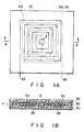
- FIG. 1A is a plan view of the planar inductor
- Fig. 1B is a sectional view taken along the line of A - A′ of Fig. 1A.
- a spiral coil 1 had a structure obtained by forming spiral conductors 2a and 2b on both surfaces of an insulating layer 3b, and electrically connecting the conductors 2a and 2b via a through hole 4. A current flowed through the conductors 2a and 2b in the same direction.
- Solid and broken lines in Fig. 1A denote the center lines of the conductors 2a and 2b located on the front and rear surfaces of the insulating layer 3b, respectively.
- Insulating layers 3a and 3c were respectively stacked on both the surfaces of the spiral coil 1, and ferromagnetic layers 5a and 5b were respectively stacked on the insulating layers 3a and 3c, thus the planar inductor was constituted.
- An inductance was formed between terminals 6a and 6b of the planar inductor including the above-mentioned members.
- Such a planar inductor was manufactured in practice, as follows. Cu foils each having a thickness of 35 »m were applied on both surfaces of a polyimide film (the insulating layer 3b) having a thickness of 25 »m, and the Cu foils were connected via the through hole 4 in a central portion to prepare a double-sided FPC board (flexible printed circuit board). The Cu foils on both the surfaces were etched to obtain the conductors 2a and 2b each having an outer size of 20 mm ⁇ 20 mm, a coil width of 250 »m, a coil pitch of 500 »m, and the number of turns of the coil of 40 (20 turns for each surface), thus manufacturing the spiral coil 1.
- Polyimide films (the insulating layers 3a and 3c) each having a thickness of 7 »m were stacked on both surfaces of the spiral coil 1, and square ferromagnetic ribbons (the ferromagnetic layers 5a and 5b) each having a side of 25 mm were further stacked on the polyimide films, respectively, thus manufacturing the planar inductor.
- a square sample having a side of 25 mm was prepared from an amorphous alloy ribbon which had a composition of (Fe 0.95 Nb 0.05 )82Si6B12, a mean thickness of 16 »m, and a width of 25 mm, and which was manufactured by a single-roll method, and the sample was used as a ferromagnetic layer.
- a square sample having a side of 25 mm was prepared from an amorphous alloy ribbon which had a composition of Fe78Si9B13, a mean thickness of 16 »m, and a width of 25 mm, and which was manufactured by a single-roll method, and the sample was used as a ferromagnetic layer.
- a square sample having a side of 25 mm was prepared from a hyperfine grain alloy ribbon obtained by thermally treating in a nitrogen atmosphere at 550°C for one hour an amorphous alloy ribbon, which had a composition of Fe 73.5 Cu1Nb3Si 13.5 B9, a mean thickness of 18 »m and a width of 25 mm, and which was manufactured by a single-roll method, and the sample was used as a ferromagnetic layer.
- a square sample having a side of 25 mm was prepared from an amorphous alloy ribbon which had a composition of (Co 0.88 Fe 0.06 Nb 0.02 Ni 0.04 )75Si10B15, a mean thickness of 16 »m, and a width of 25 mm, and which was manufactured by a single-roll method, and the sample was used as a ferromagnetic layer.
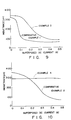
- FIG. 7 to 9 shows a relationship between a superposed DC current and an inductance of the planar inductors according to Examples 1 to 3, and Comparative Example 1.
- the inductance was measured at a frequency of 50 kHz.
- each DC superposition characteristic was largely improved as compared with that in the planar inductor in Comparative Example 1.
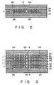
- a planar inductor shown in Fig. 2 was manufactured in Example 4 and Comparative Example 2.
- Fig. 10 shows a relationship between a superposed DC current and an inductance of the planar inductors in Example 4 and Comparative Example 2. Note that the inductance was measured at a frequency of 50 kHZ.
- Fig. 11 shows a relationship between a saturation magnetization 4 ⁇ M s of an amorphous alloy ribbon and an efficiency ⁇ of a DC-to-DC converter.
- the DC-to-DC converter was applied a planar inductor constituted of a spiral coil (thickness: about 1 mm) having an air-core inductance of 54 »H, and a coil resistance of 1.8 ⁇ , polyimide films having a thickness of 7.5 »m stacked on both surfaces of the spiral coil, and five-layered bodies of Co-or Fe-based amorphous alloy ribbons (thickness: about 15 »m) stacked on the polyimide films.
- the efficiency was measured under the conditions of an input voltage of 15 V, an output voltage of 5 V, and an output current of 0.4 A.
- the efficiency ⁇ obtained when an amorphous alloy ribbon (Js ⁇ 1 T (4 ⁇ M s ⁇ 10 kG)) was used was substantially constant, i.e., about 70%.
- an amorphous alloy ribbon (Js ⁇ 1 T (4 ⁇ M s ⁇ 10 kG)) was used, an inductance was degraded because of the superposed DC current, and the efficiency was decreased.
- Cu foils each having a thickness of 100 »m were applied on both surfaces of a polyimide film having a thickness of 25 »m, and the Cu foils were connected via a through hole in a central portion to prepare a double-sided FPC board.
- the Cu foils on both the surfaces were etched to obtain spiral conductors each having an outer size of 20 mm ⁇ 20 mm, a coil width of 250 »m, a coil pitch of 500 m, and the number of turns of the coil of 40 (20 turns for each surface), thus manufacturing the spiral coil.
- Two spiral coils were stacked with polyimide film having a thickness of 7 »m (the insulating layers 3d) interposed between the coils and the coils were electrically connected in parallel to manufacture a multi-layered coil.
- two multi-layered coils were stacked with the polyimide film (the insulating layers 3d) having a thickness of 7 »m, interposed between the multi-layered coils and the multi-layered coils were electrically connected in series to manufacture a multi-layered coil (four-layered coil).
- Polyimide films (the insulating layers 3a and 3c) each having a thickness of 7 »m were stacked on both surfaces of the multi-layered coil, and a square five-layered ferromagnetic ribbon having a side of 25 mm were further stacked on the polyimide films, thus manufacturing the planar inductor.
- the ferromagnetic ribbon has a square shape having a side of 25 mm obtained by combining a plurality of two-dimensionally divided portions, or without two-dimensionally dividing.
- Fig. 12 shows a relationship between a superposed DC current and an inductance.
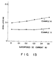
- Fig. 13 shows a relationship between a superposed DC current and an iron loss.
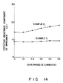
- Fig. 14 shows a relationship between a superposed DC current and an effective resistance component of an impedance.
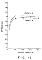
- Fig. 15 shows a relationship between an output current and an efficiency ⁇ of a noninsulated voltage-drop type DC-to-DC converter of 5-V output 2-W class, which was constituted by the planar inductors.
- Fig. 16 shows a relationship between a superposed DC current and an inductance.
- Fig. 17 shows a relationship between a superposed DC current and an iron loss.
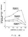
- Fig. 18 shows a relationship between a superposed DC current and an effective resistance component of an impedance.
- Fig. 19 shows a relationship between an efficiency ⁇ and an output current of a noninsulated voltage-drop type DC-to-DC converter of 5-V output 2-W class, which was constituted by the planar inductors.
- a planar inductor 20 having a four-layered coil and a five-layered ferromagnetic ribbon which had an outer size of 25 mm ⁇ 25 mm and which was manufactured in Example 6 was used.
- PPS (polyphenylenesulfide resin) films 21 each having an outer size of 30 mm ⁇ 30 mm, and a thickness of 100 »m were formed on both outer surfaces of the ferromagnetic ribbon.
- the side surfaces of the multi-layered coil were sealed with an adhesive 22 (Cemedine Super available from CEMEDINE CO., LTD.), so that when the multi-layered coil was dipped into a liquid mold resin in a subsequent step, the mold resin would not be brought into direct contact with the coil and the ferromagnetic ribbon.
- the multi-layered coil was dipped into a mold resin 23 (Ceracoat 640-43 available from Hokuriku Toso K.K.), the coil was removed from the resin. After the coil was naturally dried for about one hour, the dried coil was heated at 150°C for one hour to harden the mold resin 23, thus manufacturing a mold planar inductor.
- a mold resin 23 (Ceracoat 640-43 available from Hokuriku Toso K.K.)
- a mold planar inductor was manufactured following the same procedures as in Example 7, except for the step of forming PPS films on both outer surfaces of a ferromagnetic ribbon, and the step of sealing the side surfaces of a multi-layered coil with an adhesive.
- a planar inductor in this example had the same structure as that in Example 7, i.e., a structure having a four-layered coil and a five-layered ferromagnetic ribbon.
- the ferromagnetic ribbon consisted of square samples each having a side of 25 mm which were prepared from an amorphous alloy ribbon having a composition of (Co 0.88 Fe 0.06 Nb 0.02 Ni 0.04 )75Si10B15, a mean thickness of 16 »m, and a width of 25 mm was used, and a mold planar inductor was manufactured following the same procedures as in Example 7.
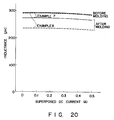
- Fig. 20 shows a relationship between a superposed DC current and an inductance before and after molding of the planar inductors in Examples 7 and 8.
- Fig. 21 shows a relationship between a superposed DC current and an inductance after molding of the planar inductors in Example 7 and Comparative Example 3.
- planar inductance element a coil having another shape such as a meander coil may be used as the planar inductance element.
Claims (15)
- Inductance planaire comprenant un élément planaire (1) d'inductance, une couche isolante (3) empilée sur chaque surface principale de l'élément d'inductance (1), et une couche ferromagnétique (5) empilée sur les surfaces principales externes des couches isolantes (3), caractérisée en ce que les couches ferromagnétiques (5) sont divisées en plusieurs parties, dans une vue en plan des couches (5), et l'épaisseur des couches ferromagnétiques (5) ne dépasse pas 100 »m.
- Inductance planaire selon la revendication 1, caractérisée en ce que l'aimantation à saturation (4πMs) des couches ferromagnétiques (5) n'est pas inférieure à 1 T (10 kG).
- Inductance planaire selon la revendication 1 ou 2, caractérisée en ce que l'épaisseur des couches ferromagnétiques (5) n'est pas inférieure à 4 »m.
- Inductance planaire selon l'une quelconque des revendications 1 à 3, caractérisée en ce que la perméabilité efficace »10k a une fréquence de 10 kHz des couches ferromagnétiques (5) n'est pas inférieure à 1.10⁴.
- Inductance planaire selon l'une quelconque des revendications 1 à 4, caractérisée en ce que les couches ferromagnétiques (5) sont formées d'un ruban d'alliage amorphe représenté par la formule suivante :

- Inductance planaire selon l'une quelconque des revendication 1 à 5, caractérisée en ce que les couches ferromagnétiques (5) sont formées d'un ruban d'alliage à grain superfin obtenu par traitement thermique d'un ruban d'alliage amorphe à base de Fe à une température supérieure à une température de cristallisation.
- Inductance planaire selon l'une quelconque des revendications 1 à 6, caractérisée en ce que l'élément (1) d'inductance planaire est une bobine spiralée.
- Inductance planaire selon l'une quelconque des revendications 1 à 7, caractérisée en ce que l'élément d'inductance planaire (1) comporte un empilement de bobines spiralées ayant des couches isolantes (3d) disposées entre elles, les couches ferromagnétiques étant empilées sur les couches isolantes externes.
- Inductance planaire selon l'une quelconque des revendications 1 à 8, caractérisée en ce qu'une couche (21) de relaxation destinée à la contraction d'une résine de moulage (23) est formée sur les couches ferromagnétiques (5), et la totalité des organes est revêtue de la résine de moulage (23).
- Inductance planaire selon la revendication 9, caractérisée en ce que la couche de relaxation (21) est formée d'un film d'un polymère organique dont la température de déformation thermique est supérieure à la température de durcissement de la résine de moulage (23).
- Inductance planaire selon la revendication 10, caractérisée en ce que le film d'un polymère organique est formé de sulfure de polyphénylène.
- Inductance planaire selon la revendication 10, caractérisée en ce que l'épaisseur du film polymère organique est inférieure à 20 »m.
- Inductance planaire selon la revendication 1, caractérisée en ce que plusieurs couches ferromagnétiques (5) sont empilées sur la grande face externe de chacune des couches isolantes (3).
- Convertisseur continu-continu comprenant une inductance planaire, l'inductance planaire comprenant un élément d'inductance planaire (1), une couche isolante (3) empilée sur chaque grande face de l'élément d'inductance (1), et une couche ferromagnétique (5) empilée sur les grandes faces externes principales des couches isolantes (3), caractérisé en ce que les couches ferromagnétiques (5) sont divisées en plusieurs parties, dans une vue en plan des couches (5), et l'épaisseur des couches ferromagnétiques (5) ne dépasse pas 100 »m.
- Convertisseur continu-continu selon la revendication 14, caractérisé en ce que plusieurs couches ferromagnétiques (5) sont empilées sur la grande face externe de chacune des couches isolantes (3).
Applications Claiming Priority (6)
| Application Number | Priority Date | Filing Date | Title |
|---|---|---|---|
| JP24643288 | 1988-09-30 | ||
| JP246432/88 | 1988-09-30 | ||
| JP24643388 | 1988-09-30 | ||
| JP246433/88 | 1988-09-30 | ||
| JP1461389 | 1989-01-24 | ||
| JP14613/89 | 1989-01-24 |
Publications (2)
| Publication Number | Publication Date |
|---|---|
| EP0361967A1 EP0361967A1 (fr) | 1990-04-04 |
| EP0361967B1 true EP0361967B1 (fr) | 1995-12-20 |
Family
ID=27280710
Family Applications (1)
| Application Number | Title | Priority Date | Filing Date |
|---|---|---|---|
| EP89309998A Expired - Lifetime EP0361967B1 (fr) | 1988-09-30 | 1989-09-29 | Inductivité plane |
Country Status (3)
| Country | Link |
|---|---|
| US (2) | US6175293B1 (fr) |
| EP (1) | EP0361967B1 (fr) |
| DE (1) | DE68925171T2 (fr) |
Families Citing this family (41)
| Publication number | Priority date | Publication date | Assignee | Title |
|---|---|---|---|---|
| KR960006848B1 (ko) * | 1990-05-31 | 1996-05-23 | 가부시끼가이샤 도시바 | 평면형 자기소자 |
| JP3116713B2 (ja) * | 1994-03-31 | 2000-12-11 | 株式会社村田製作所 | インダクタ内蔵電子部品 |
| DE19522043A1 (de) * | 1995-06-17 | 1996-12-19 | Bosch Gmbh Robert | Induktives Bauelement |
| KR100246287B1 (ko) * | 1996-10-25 | 2000-03-15 | 김영남 | 음극선관용 필름형 새들타입 편향부재의 도선의 패턴 배열방법 및 이에 의한 도선배열구조의 필름형 새들타입 편향부재 |
| JPH11273949A (ja) * | 1998-03-24 | 1999-10-08 | Tif:Kk | インダクタ素子 |
| US6700472B2 (en) * | 2001-12-11 | 2004-03-02 | Intersil Americas Inc. | Magnetic thin film inductors |
| JP3634305B2 (ja) | 2001-12-14 | 2005-03-30 | 三菱電機株式会社 | 積層インダクタンス素子 |
| US7259639B2 (en) * | 2002-03-29 | 2007-08-21 | M/A-Com Eurotec, B.V. | Inductor topologies and decoupling structures for filters used in broadband applications, and design methodology thereof |
| WO2004019352A1 (fr) * | 2002-08-26 | 2004-03-04 | Matsushita Electric Industrial Co., Ltd. | Element magnetique a utilisation multiphase et procede de production correspondant |
| US20050077992A1 (en) * | 2002-09-20 | 2005-04-14 | Gopal Raghavan | Symmetric planar inductor |
| WO2004079795A2 (fr) * | 2003-03-04 | 2004-09-16 | Rohm And Haas Electronic Materials, L.L.C. | Microstructures a guide d'ondes coaxial et leur procede de formation |
| US7126443B2 (en) | 2003-03-28 | 2006-10-24 | M/A-Com, Eurotec, B.V. | Increasing performance of planar inductors used in broadband applications |
| EP1661053A4 (fr) * | 2003-08-08 | 2012-06-13 | Shmuel Shapira | Systeme et procede de formation de circuit |
| US6998952B2 (en) * | 2003-12-05 | 2006-02-14 | Freescale Semiconductor, Inc. | Inductive device including bond wires |
| US9105391B2 (en) * | 2006-08-28 | 2015-08-11 | Avago Technologies General Ip (Singapore) Pte. Ltd. | High voltage hold-off coil transducer |
| US8427844B2 (en) * | 2006-08-28 | 2013-04-23 | Avago Technologies Ecbu Ip (Singapore) Pte. Ltd. | Widebody coil isolators |
| US8061017B2 (en) * | 2006-08-28 | 2011-11-22 | Avago Technologies Ecbu Ip (Singapore) Pte. Ltd. | Methods of making coil transducers |
| US7948067B2 (en) * | 2009-06-30 | 2011-05-24 | Avago Technologies Ecbu Ip (Singapore) Pte. Ltd. | Coil transducer isolator packages |
| US20080278275A1 (en) * | 2007-05-10 | 2008-11-13 | Fouquet Julie E | Miniature Transformers Adapted for use in Galvanic Isolators and the Like |
| US7852186B2 (en) * | 2006-08-28 | 2010-12-14 | Avago Technologies Ecbu Ip (Singapore) Pte. Ltd. | Coil transducer with reduced arcing and improved high voltage breakdown performance characteristics |
| US8385043B2 (en) * | 2006-08-28 | 2013-02-26 | Avago Technologies ECBU IP (Singapoare) Pte. Ltd. | Galvanic isolator |
| US8093983B2 (en) * | 2006-08-28 | 2012-01-10 | Avago Technologies Ecbu Ip (Singapore) Pte. Ltd. | Narrowbody coil isolator |
| US7791900B2 (en) * | 2006-08-28 | 2010-09-07 | Avago Technologies General Ip (Singapore) Pte. Ltd. | Galvanic isolator |
| US9019057B2 (en) * | 2006-08-28 | 2015-04-28 | Avago Technologies General Ip (Singapore) Pte. Ltd. | Galvanic isolators and coil transducers |
| US7524731B2 (en) * | 2006-09-29 | 2009-04-28 | Freescale Semiconductor, Inc. | Process of forming an electronic device including an inductor |
| US8143986B2 (en) * | 2007-01-24 | 2012-03-27 | Renesas Electronics Corporation | Inductor |
| US8258911B2 (en) | 2008-03-31 | 2012-09-04 | Avago Technologies ECBU IP (Singapor) Pte. Ltd. | Compact power transformer components, devices, systems and methods |
| US9141157B2 (en) * | 2011-10-13 | 2015-09-22 | Texas Instruments Incorporated | Molded power supply system having a thermally insulated component |
| US20150173380A1 (en) * | 2012-07-06 | 2015-06-25 | Pier RUBESA | Method and apparatus for the amplification of electrical charges in biological systems or bioactive matter using an inductive disk with a fixed geometric trace |
| JP6170568B2 (ja) * | 2012-12-19 | 2017-07-26 | テレフオンアクチーボラゲット エルエム エリクソン(パブル) | 平面トランス |
| DE102013100622B4 (de) * | 2013-01-22 | 2018-03-01 | Phoenix Contact Gmbh & Co. Kg | Leiterplatte im Lagenaufbau |
| US9799448B2 (en) * | 2013-10-03 | 2017-10-24 | Power Gold LLC | Inductor, transformer, and method |
| JP6678292B2 (ja) * | 2015-02-19 | 2020-04-08 | パナソニックIpマネジメント株式会社 | コモンモードノイズフィルタ |
| CN106531410B (zh) * | 2015-09-15 | 2019-08-27 | 臻绚电子科技(上海)有限公司 | 线圈,电感元件及制备应用于电感元件的线圈的方法 |
| US10283257B2 (en) * | 2016-01-08 | 2019-05-07 | Qualcomm Incorporated | Skewed co-spiral inductor structure |
| US20180001269A1 (en) * | 2016-06-30 | 2018-01-04 | L'air Liquide, Societe Anonyme Pour L'etude Et L'exploitation Des Procedes Georges Claude | Metallopolyimide precursor fibers for aging-resistant carbon molecular sieve hollow fiber membranes with enhanced selectivity |
| JP2018019062A (ja) * | 2016-07-27 | 2018-02-01 | サムソン エレクトロ−メカニックス カンパニーリミテッド. | インダクタ |
| WO2019099011A1 (fr) * | 2017-11-16 | 2019-05-23 | Georgia Tech Research Corporation | Bobines d'induction compatibles avec un substrat avec des couches magnétiques |
| KR102554936B1 (ko) * | 2018-04-13 | 2023-07-12 | 현대자동차주식회사 | 평면 변압기 |
| US11348718B2 (en) * | 2018-06-29 | 2022-05-31 | Intel Corporation | Substrate embedded magnetic core inductors and method of making |
| CN113394014B (zh) * | 2021-06-09 | 2023-02-03 | 珠海市日创工业自动化设备有限公司 | 一种变压器引脚浸锡装置 |
Citations (2)
| Publication number | Priority date | Publication date | Assignee | Title |
|---|---|---|---|---|
| US4494100A (en) * | 1982-07-12 | 1985-01-15 | Motorola, Inc. | Planar inductors |
| EP0271657A2 (fr) * | 1986-12-15 | 1988-06-22 | Hitachi Metals, Ltd. | Alliage magnétiquement doux à base de fer et méthode de fabrication |
Family Cites Families (13)
| Publication number | Priority date | Publication date | Assignee | Title |
|---|---|---|---|---|
| US3798059A (en) * | 1970-04-20 | 1974-03-19 | Rca Corp | Thick film inductor with ferromagnetic core |
| US3833872A (en) * | 1972-06-13 | 1974-09-03 | I Marcus | Microminiature monolithic ferroceramic transformer |
| JPS4978876A (fr) | 1972-12-09 | 1974-07-30 | ||
| US4021705A (en) * | 1975-03-24 | 1977-05-03 | Lichtblau G J | Resonant tag circuits having one or more fusible links |
| GB2045540B (en) * | 1978-12-28 | 1983-08-03 | Tdk Electronics Co Ltd | Electrical inductive device |
| JPS5814512A (ja) | 1981-07-17 | 1983-01-27 | Sanyo Electric Co Ltd | インダクタ素子 |
| JPS58133906A (ja) | 1982-02-03 | 1983-08-09 | Mitsubishi Steel Mfg Co Ltd | 親子板ばねの支持方法及び親子板ばね |
| JPS5967909A (ja) | 1982-10-09 | 1984-04-17 | 三浦 公亮 | 伸展構造物 |
| JPS616817A (ja) * | 1984-06-20 | 1986-01-13 | Canon Inc | シ−トコイルの製造方法 |
| US4613843A (en) * | 1984-10-22 | 1986-09-23 | Ford Motor Company | Planar coil magnetic transducer |
| JPH0746660B2 (ja) | 1985-09-30 | 1995-05-17 | 株式会社東芝 | 薄形トランス |
| US4959631A (en) * | 1987-09-29 | 1990-09-25 | Kabushiki Kaisha Toshiba | Planar inductor |
| DE3908896C2 (de) * | 1988-03-17 | 1994-02-24 | Murata Manufacturing Co | Chipinduktor |
-
1989
- 1989-09-29 DE DE68925171T patent/DE68925171T2/de not_active Expired - Fee Related
- 1989-09-29 EP EP89309998A patent/EP0361967B1/fr not_active Expired - Lifetime
-
1993
- 1993-05-11 US US08/059,350 patent/US6175293B1/en not_active Expired - Fee Related
-
2000
- 2000-11-21 US US09/716,403 patent/US6466122B1/en not_active Expired - Fee Related
Patent Citations (2)
| Publication number | Priority date | Publication date | Assignee | Title |
|---|---|---|---|---|
| US4494100A (en) * | 1982-07-12 | 1985-01-15 | Motorola, Inc. | Planar inductors |
| EP0271657A2 (fr) * | 1986-12-15 | 1988-06-22 | Hitachi Metals, Ltd. | Alliage magnétiquement doux à base de fer et méthode de fabrication |
Non-Patent Citations (1)
| Title |
|---|
| Electrische Machines 1A, page 3.47, Technical University Delft, July 1983 * |
Also Published As
| Publication number | Publication date |
|---|---|
| DE68925171T2 (de) | 1996-06-05 |
| US6175293B1 (en) | 2001-01-16 |
| US6466122B1 (en) | 2002-10-15 |
| EP0361967A1 (fr) | 1990-04-04 |
| DE68925171D1 (de) | 1996-02-01 |
Similar Documents
| Publication | Publication Date | Title |
|---|---|---|
| EP0361967B1 (fr) | Inductivité plane | |
| US7289013B2 (en) | Bulk amorphous metal inductive device | |
| US6737951B1 (en) | Bulk amorphous metal inductive device | |
| KR910003292B1 (ko) | 평면인덕터 | |
| KR100255485B1 (ko) | 박형 자기소자 및 트랜스 | |
| JP3688732B2 (ja) | 平面型磁気素子および非晶質磁性薄膜 | |
| US7570223B2 (en) | Antenna core and method for production of an antenna core | |
| EP1679727A1 (fr) | Dispositif inductif et procede de fabrication associe | |
| JP2002158112A (ja) | 微小インダクタや微小変圧器といったタイプの微小素子 | |
| WO2002011158A2 (fr) | Composant magnetique metallique rapporte de haute performance | |
| JPS6234122B2 (fr) | ||
| JP2735295B2 (ja) | 平面インダクタ | |
| JPH05275247A (ja) | 薄形インダクタ/トランス | |
| JP3540733B2 (ja) | 平面型磁気素子及びそれを用いた半導体装置 | |
| EP0337716B1 (fr) | Ruban magnétique et noyau magnétique | |
| JP3373350B2 (ja) | 磁性部品およびその製法 | |
| JP2005109246A (ja) | 高周波用磁性薄膜、その作製方法及び磁気素子 | |
| JPH03276604A (ja) | 平面インダクタ | |
| JPH10289821A (ja) | 高周波帯域用磁気デバイス | |
| JP2958893B2 (ja) | 平面インダクタ | |
| Shirakawa et al. | Thin film inductor with multilayer magnetic core | |
| JPH10270253A (ja) | インダクタンス素子及びlc複合素子 | |
| JPH01157508A (ja) | 平面インダクタ | |
| JP2633813B2 (ja) | スイッチング回路用リアクトルの製造方法 | |
| JPH07201602A (ja) | 平面型磁気素子 |
Legal Events
| Date | Code | Title | Description |
|---|---|---|---|
| PUAI | Public reference made under article 153(3) epc to a published international application that has entered the european phase |
Free format text: ORIGINAL CODE: 0009012 |
|
| 17P | Request for examination filed |
Effective date: 19891025 |
|
| AK | Designated contracting states |
Kind code of ref document: A1 Designated state(s): DE FR GB |
|
| 17Q | First examination report despatched |
Effective date: 19920219 |
|
| GRAA | (expected) grant |
Free format text: ORIGINAL CODE: 0009210 |
|
| AK | Designated contracting states |
Kind code of ref document: B1 Designated state(s): DE FR GB |
|
| REF | Corresponds to: |
Ref document number: 68925171 Country of ref document: DE Date of ref document: 19960201 |
|
| ET | Fr: translation filed | ||
| PLBE | No opposition filed within time limit |
Free format text: ORIGINAL CODE: 0009261 |
|
| STAA | Information on the status of an ep patent application or granted ep patent |
Free format text: STATUS: NO OPPOSITION FILED WITHIN TIME LIMIT |
|
| 26N | No opposition filed | ||
| REG | Reference to a national code |
Ref country code: GB Ref legal event code: 746 Effective date: 19980915 |
|
| REG | Reference to a national code |
Ref country code: FR Ref legal event code: D6 |
|
| REG | Reference to a national code |
Ref country code: GB Ref legal event code: IF02 |
|
| PGFP | Annual fee paid to national office [announced via postgrant information from national office to epo] |
Ref country code: DE Payment date: 20070927 Year of fee payment: 19 |
|
| PGFP | Annual fee paid to national office [announced via postgrant information from national office to epo] |
Ref country code: GB Payment date: 20070926 Year of fee payment: 19 |
|
| PGFP | Annual fee paid to national office [announced via postgrant information from national office to epo] |
Ref country code: FR Payment date: 20070914 Year of fee payment: 19 |
|
| GBPC | Gb: european patent ceased through non-payment of renewal fee |
Effective date: 20080929 |
|
| REG | Reference to a national code |
Ref country code: FR Ref legal event code: ST Effective date: 20090529 |
|
| PG25 | Lapsed in a contracting state [announced via postgrant information from national office to epo] |
Ref country code: DE Free format text: LAPSE BECAUSE OF NON-PAYMENT OF DUE FEES Effective date: 20090401 |
|
| PG25 | Lapsed in a contracting state [announced via postgrant information from national office to epo] |
Ref country code: FR Free format text: LAPSE BECAUSE OF NON-PAYMENT OF DUE FEES Effective date: 20080930 |
|
| PG25 | Lapsed in a contracting state [announced via postgrant information from national office to epo] |
Ref country code: GB Free format text: LAPSE BECAUSE OF NON-PAYMENT OF DUE FEES Effective date: 20080929 |