EP0361779A1 - Mikrostreifenarchitektur für Membrantestsonde - Google Patents
Mikrostreifenarchitektur für Membrantestsonde Download PDFInfo
- Publication number
- EP0361779A1 EP0361779A1 EP89309587A EP89309587A EP0361779A1 EP 0361779 A1 EP0361779 A1 EP 0361779A1 EP 89309587 A EP89309587 A EP 89309587A EP 89309587 A EP89309587 A EP 89309587A EP 0361779 A1 EP0361779 A1 EP 0361779A1
- Authority
- EP
- European Patent Office
- Prior art keywords
- membrane
- ground
- contact
- trace
- via hole
- Prior art date
- Legal status (The legal status is an assumption and is not a legal conclusion. Google has not performed a legal analysis and makes no representation as to the accuracy of the status listed.)
- Withdrawn
Links
Images

Classifications
-
- G—PHYSICS
- G01—MEASURING; TESTING
- G01R—MEASURING ELECTRIC VARIABLES; MEASURING MAGNETIC VARIABLES
- G01R1/00—Details of instruments or arrangements of the types included in groups G01R5/00 - G01R13/00 and G01R31/00
- G01R1/02—General constructional details
- G01R1/06—Measuring leads; Measuring probes
- G01R1/067—Measuring probes
- G01R1/06711—Probe needles; Cantilever beams; "Bump" contacts; Replaceable probe pins
-
- G—PHYSICS
- G01—MEASURING; TESTING
- G01R—MEASURING ELECTRIC VARIABLES; MEASURING MAGNETIC VARIABLES
- G01R1/00—Details of instruments or arrangements of the types included in groups G01R5/00 - G01R13/00 and G01R31/00
- G01R1/02—General constructional details
- G01R1/06—Measuring leads; Measuring probes
- G01R1/067—Measuring probes
- G01R1/073—Multiple probes
- G01R1/07307—Multiple probes with individual probe elements, e.g. needles, cantilever beams or bump contacts, fixed in relation to each other, e.g. bed of nails fixture or probe card
- G01R1/0735—Multiple probes with individual probe elements, e.g. needles, cantilever beams or bump contacts, fixed in relation to each other, e.g. bed of nails fixture or probe card arranged on a flexible frame or film
-
- G—PHYSICS
- G01—MEASURING; TESTING
- G01R—MEASURING ELECTRIC VARIABLES; MEASURING MAGNETIC VARIABLES
- G01R1/00—Details of instruments or arrangements of the types included in groups G01R5/00 - G01R13/00 and G01R31/00
- G01R1/02—General constructional details
- G01R1/18—Screening arrangements against electric or magnetic fields, e.g. against earth's field
Definitions
- This invention relates generally to the field of semiconductor testing, and more specifically to test probes used for testing a semiconductor device under test (DUT).
- DUT semiconductor device under test
- Non-destructive methods for testing integrated circuits are known to people skilled in the art of semiconductor fabrication. Integrated circuits are generally grown layer by layer on thin planar substrates called wafers; many chips are formed on one wafer. Before the wafer is cut into individual chips that are then encapsulated within protective packages to create finished products, the circuitry must be inspected and checked.
- Testing is usually performed while the chip circuit dies still reside together on a single wafer, since testing after the dies have been sawn apart and packaged is prohibitively expensive. Hundreds of separate chip devices on every wafer are analyzed by passing input signals into each chip device and monitoring voltage levels at selected output locations on the tiny circuits.
- test probes are used to check these chip circuits while they still reside together on a wafer. These test probes often produce inaccurate results when tests are conducted using very high speed input signals.
- Previous test equipment incorporates a probe card that holds a flexible membrane which in turn supports a set of microst rip traces for conducting signals through a contact from a test device. This conventional tester, however, has signal traces on the same side of the membrane as the contact which touches the device under test.
- the electrical test signals produced on the probe card are not shielded from electromagnetic and electrical interference caused by active electronic components residing on the test device.
- Capacitive and inductive coupling between the signal traces on the membrane and the circuitry on the test wafer can distort measurements taken during an examination procedure.
- an even more problem with a probe card is that the unshielded circuit can physically touch the input-output pads of the chip die adjacent to the chip die device under test. Besides compromising the accuracy of the test measurements, an accidental contact can damage the adjacent chip die by causing for example an electrical short circuit.
- the present invention offers a test system capable of delivering high speed test signals to integrated circuit chips already formed on a wafer.
- the design used by the inventors provides reliable test results (a) by minimizing signal distortion and (b) by preventing interference and accidental contact between a test circuit and a device under test.
- the invention is primarily intended for use as part of an automated test system, it can be used in any environment in which accurate test measurements must be obtained using high frequency test signals.
- This invention overcomes the existing problem of high signal distortion common to high speed testing of integrated circuits.
- the invention can be used in conjunction with a conventional probe card held in a stationary chuck while a test wafer is stepped beneath the probe on a moving chuck.
- This invention includes a flexible membrane held by a carrier.
- the membrane supports a pattern of electric current conducting signal traces, also called electric current paths, formed on its upper surface.
- a ground plane deposited on the opposite lower side of the membrane faces toward the integrated circuits residing on a wafer that require analysis. The ground plane helps reduce crosstalk between the test device and the signal traces.
- Electrical contact bumps connected to the signal traces through perforations in the membrane are used to impinge upon input and output pads associated with the test device. These bumps are formed by plating through via holes in the membrane so that they protrude past the ground plane and extend in the direction of the device under test.
- This invention provides a reliable and accurate system for analyzing circuits on an integrated circuit that will enable engineers in the semiconductor industry to construct better and more economical test equipment.
- the Claims define; in contrast, the Drawings, Detailed Description and Abstract illustrate an example.
- the Claims broadly define the invention, an invention which can be practiced using many different example structures.
- the Drawings, Detailed Description and Abstract present a single specific example structure, with parts identified by reference numbers, built according to the broadlyt claimed invention.
- this invention offers a system for establishing electrical contact with a device under test (DUT) (not shown).
- DUT device under test
- the inventive membrane test probe system 10 includes a first conductor 14 and a second conductor 25.
- a planar means 12 is provided and has a first surface designed for being coupled to the first conductor and the second conductor. Further, planar means 12 has a second surface, and a first and a second perforation 17, 23 through itself. Planar means 12 is formed to be flexible.
- a shield 16 formed to function as an electromagnetic interference minimization means, and formed to be coupled to the second surface of the planar means.
- a first contact means 18 is formed for being placed into contact with the device under test and formed for being electrically coupled to the first conductor 14 while substantially filling the first perforation 17 and protruding past the second surface.
- a second contact means 24 is placed into contact with the device under test. Means 24 is coupled to second conductor 25 while substantially filling second perforation 23 and protruding past the second surface.
- Figure 1 shows an example construction memnbrane test probe 10 in cross-section.
- a flexible membrane 12 is suspended by a carrier (not shown) and supports a pattern of signal traces 14 on its upper surface and a pattern of ground planes 16 on its lower surface.
- Via holes 17 provide channels through membrane 12 for connection to signal traces 14 and for formation of contact bumps 18.
- the contact bumps 18 are guided by test probe 10 over a device under test 20.
- the test device 20 typically a wafer comprising a great number of integrated circuits, includes many input and output pads 22 which are the targets of contact bumps 18.
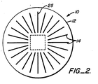
- Figure 2 reveals a top plan view of the membrane 12 and signal trace pattern 14 shown in Figure 1.
- Figures 3, 4, and 5 illustrate progressive views of the probe 10 as it is fabricated.
- a pattern of signal traces 14 has been formed lithographically on the upper side of perforated membrane 12.
- an insulative polyimide material was used for the membrane 12.
- the widths of the traces 14 are selected so that the required line impedance is achieved once the ground planes 16 have been added.
- a pattern of perforations is then produced by conventional laser micro-machining techniques using an excimer laser (not shown). Some of the perforations through the membrane 12 will be used as via holes 17 for contact bumps 18, while others will serve as ground plane via holes 23 for ground contact bumps 24.
- the contact bump via holes 17 are located at the end of signal traces 14. Similarly, a second set of via holes 23 for ground planes 16 are placed where ground planes 16 must be coupled to ground contact bumps 24 and to a pattern of ground traces 25 that may be deposited on the upper surface of the membrane 12 in an alternating or interleaved configuration along with signal traces 14.
- Both sets of holes 17 and 23 are then filled with a conductive metal to fabricate generally hemispherical or "mushroom” shaped protrusions that extend past the ground planes 16.
- the flexible membrane 12 serves as its own plating mask.
- the ground plane pattern 16 is then deposited on the bottom side of membrane 12 as shown in Figure 5.
- This last step couples the ground bumps 24 and ground planes 16 through ground vias 23 to ground traces 25 so that common mode ground impedance is minimized.
- the photolithographic fabrication processes that are used to place signal and ground patterns on membrane 12 are well known to persons ordinarily skilled in the semiconductor art.
- Micro-Strip Architecture claimed below may be used in conjunction with an Improved Membrane Precision Probe that is held in a stationary chuck while a test wafer is stepped beneath the probe on a moving chuck.
Applications Claiming Priority (2)
| Application Number | Priority Date | Filing Date | Title |
|---|---|---|---|
| US24947488A | 1988-09-26 | 1988-09-26 | |
| US249474 | 1988-09-26 |
Publications (1)
| Publication Number | Publication Date |
|---|---|
| EP0361779A1 true EP0361779A1 (de) | 1990-04-04 |
Family
ID=22943616
Family Applications (1)
| Application Number | Title | Priority Date | Filing Date |
|---|---|---|---|
| EP89309587A Withdrawn EP0361779A1 (de) | 1988-09-26 | 1989-09-20 | Mikrostreifenarchitektur für Membrantestsonde |
Country Status (2)
| Country | Link |
|---|---|
| EP (1) | EP0361779A1 (de) |
| JP (1) | JPH02141681A (de) |
Cited By (19)
| Publication number | Priority date | Publication date | Assignee | Title |
|---|---|---|---|---|
| GB2239744A (en) * | 1989-11-07 | 1991-07-10 | Sharp Kk | Testing L.C.D. displays; flexible test circuit contacts |
| US5090118A (en) * | 1990-07-31 | 1992-02-25 | Texas Instruments Incorporated | High performance test head and method of making |
| US5621333A (en) * | 1995-05-19 | 1997-04-15 | Microconnect, Inc. | Contact device for making connection to an electronic circuit device |
| EP0768712A2 (de) * | 1995-10-13 | 1997-04-16 | Meiko Electronics Co., Ltd. | Höckerkontakt für eine Leiterplatte und Halbleitermodul mit derselben |
| US5623213A (en) * | 1994-09-09 | 1997-04-22 | Micromodule Systems | Membrane probing of circuits |
| US5847571A (en) * | 1994-09-09 | 1998-12-08 | Micromodule Systems | Membrane probing of circuits |
| EP0902296A1 (de) * | 1997-09-11 | 1999-03-17 | Photo Print Electronic GmbH | Adapteranordnungen zum Testen von Leiterplatten |
| US5973504A (en) * | 1994-10-28 | 1999-10-26 | Kulicke & Soffa Industries, Inc. | Programmable high-density electronic device testing |
| US6046599A (en) * | 1996-05-20 | 2000-04-04 | Microconnect, Inc. | Method and device for making connection |
| US6343369B1 (en) | 1998-09-15 | 2002-01-29 | Microconnect, Inc. | Methods for making contact device for making connection to an electronic circuit device and methods of using the same |
| US6496026B1 (en) | 2000-02-25 | 2002-12-17 | Microconnect, Inc. | Method of manufacturing and testing an electronic device using a contact device having fingers and a mechanical ground |
| EP1509776A2 (de) * | 2002-05-23 | 2005-03-02 | Cascade Microtech, Inc. | Sonde zum testen einer zu testenden einrichtung |
| EP1627235A2 (de) * | 2003-05-23 | 2006-02-22 | Cascade Microtech, Inc. | Sonde zum testen eines zu prüfenden bausteins |
| US9435855B2 (en) | 2013-11-19 | 2016-09-06 | Teradyne, Inc. | Interconnect for transmitting signals between a device and a tester |
| US9594114B2 (en) | 2014-06-26 | 2017-03-14 | Teradyne, Inc. | Structure for transmitting signals in an application space between a device under test and test electronics |
| US9977052B2 (en) | 2016-10-04 | 2018-05-22 | Teradyne, Inc. | Test fixture |
| US10677815B2 (en) | 2018-06-08 | 2020-06-09 | Teradyne, Inc. | Test system having distributed resources |
| US11363746B2 (en) | 2019-09-06 | 2022-06-14 | Teradyne, Inc. | EMI shielding for a signal trace |
| US11862901B2 (en) | 2020-12-15 | 2024-01-02 | Teradyne, Inc. | Interposer |
Families Citing this family (2)
| Publication number | Priority date | Publication date | Assignee | Title |
|---|---|---|---|---|
| US7707992B2 (en) * | 2003-10-31 | 2010-05-04 | Woodward Governor Company | Method and apparatus for controlling exhaust gas recirculation and start of combustion in reciprocating compression ignition engines with an ignition system with ionization measurement |
| US7420381B2 (en) | 2004-09-13 | 2008-09-02 | Cascade Microtech, Inc. | Double sided probing structures |
Citations (3)
| Publication number | Priority date | Publication date | Assignee | Title |
|---|---|---|---|---|
| DE2021879A1 (de) * | 1969-05-29 | 1970-12-03 | Ibm | Membranschalter |
| EP0230348A2 (de) * | 1986-01-07 | 1987-07-29 | Hewlett-Packard Company | Testsonde |
| EP0294939A2 (de) * | 1987-06-09 | 1988-12-14 | Tektronix Inc. | Vielfachsonde für integrierte Schaltkreise in Scheibenform |
-
1989
- 1989-09-20 EP EP89309587A patent/EP0361779A1/de not_active Withdrawn
- 1989-09-22 JP JP24786089A patent/JPH02141681A/ja active Pending
Patent Citations (3)
| Publication number | Priority date | Publication date | Assignee | Title |
|---|---|---|---|---|
| DE2021879A1 (de) * | 1969-05-29 | 1970-12-03 | Ibm | Membranschalter |
| EP0230348A2 (de) * | 1986-01-07 | 1987-07-29 | Hewlett-Packard Company | Testsonde |
| EP0294939A2 (de) * | 1987-06-09 | 1988-12-14 | Tektronix Inc. | Vielfachsonde für integrierte Schaltkreise in Scheibenform |
Cited By (35)
| Publication number | Priority date | Publication date | Assignee | Title |
|---|---|---|---|---|
| GB2239744B (en) * | 1989-11-07 | 1994-03-16 | Sharp Kk | Tester head |
| GB2239744A (en) * | 1989-11-07 | 1991-07-10 | Sharp Kk | Testing L.C.D. displays; flexible test circuit contacts |
| US5090118A (en) * | 1990-07-31 | 1992-02-25 | Texas Instruments Incorporated | High performance test head and method of making |
| US5841291A (en) * | 1994-09-09 | 1998-11-24 | Micromodule Systems | Exchangeable membrane probe testing of circuits |
| US5847571A (en) * | 1994-09-09 | 1998-12-08 | Micromodule Systems | Membrane probing of circuits |
| US5623213A (en) * | 1994-09-09 | 1997-04-22 | Micromodule Systems | Membrane probing of circuits |
| EP0779989A1 (de) * | 1994-09-09 | 1997-06-25 | Micromodule Systems, Inc. | Abtasten von schaltkreisen mit einem membranfühler |
| EP0779989A4 (de) * | 1994-09-09 | 1998-01-07 | Micromodule Systems Inc | Abtasten von schaltkreisen mit einem membranfühler |
| US5973504A (en) * | 1994-10-28 | 1999-10-26 | Kulicke & Soffa Industries, Inc. | Programmable high-density electronic device testing |
| US6091256A (en) * | 1995-05-19 | 2000-07-18 | Microconnect, Inc. | Contact device for making connection to an electronic circuit device |
| US5621333A (en) * | 1995-05-19 | 1997-04-15 | Microconnect, Inc. | Contact device for making connection to an electronic circuit device |
| EP0768712A2 (de) * | 1995-10-13 | 1997-04-16 | Meiko Electronics Co., Ltd. | Höckerkontakt für eine Leiterplatte und Halbleitermodul mit derselben |
| EP0768712A3 (de) * | 1995-10-13 | 1999-01-07 | Meiko Electronics Co., Ltd. | Höckerkontakt für eine Leiterplatte und Halbleitermodul mit derselben |
| US6350957B1 (en) | 1995-10-13 | 2002-02-26 | Meiko Electronics, Co., Ltd. | Circuit board, manufacturing method therefor, and bump-type contact head and semiconductor component packaging module using the circuit board |
| US6239983B1 (en) | 1995-10-13 | 2001-05-29 | Meiko Electronics Co., Ltd. | Circuit board, manufacturing method therefor, and bump-type contact head and semiconductor component packaging module using the circuit board |
| US6046599A (en) * | 1996-05-20 | 2000-04-04 | Microconnect, Inc. | Method and device for making connection |
| EP0902296A1 (de) * | 1997-09-11 | 1999-03-17 | Photo Print Electronic GmbH | Adapteranordnungen zum Testen von Leiterplatten |
| US6343369B1 (en) | 1998-09-15 | 2002-01-29 | Microconnect, Inc. | Methods for making contact device for making connection to an electronic circuit device and methods of using the same |
| US6622289B2 (en) | 1998-09-15 | 2003-09-16 | Microconnect, Llc | Methods for making contact device for making connection to an electronic circuit device and methods of using the same |
| US6957405B2 (en) | 1998-09-15 | 2005-10-18 | Microconnect Llc | Methods for manufacturing an electronic device having an electronically determined physical test member |
| US8756537B2 (en) | 1998-09-15 | 2014-06-17 | Microconnect Corp. | Methods for making contact device for making connection to an electronic circuit device and methods using the same |
| US7386816B2 (en) | 1998-09-15 | 2008-06-10 | Microconnect Llc | Method for manufacturing an electronic device having an electronically determined physical test member |
| US8056031B2 (en) | 1998-09-15 | 2011-11-08 | Microconnect Corp. | Methods for manufacturing an electronic device using an electronically determined test member |
| US6496026B1 (en) | 2000-02-25 | 2002-12-17 | Microconnect, Inc. | Method of manufacturing and testing an electronic device using a contact device having fingers and a mechanical ground |
| EP1509776A2 (de) * | 2002-05-23 | 2005-03-02 | Cascade Microtech, Inc. | Sonde zum testen einer zu testenden einrichtung |
| EP1509776A4 (de) * | 2002-05-23 | 2010-08-18 | Cascade Microtech Inc | Sonde zum testen einer zu testenden einrichtung |
| US7898273B2 (en) | 2003-05-23 | 2011-03-01 | Cascade Microtech, Inc. | Probe for testing a device under test |
| EP1627235A4 (de) * | 2003-05-23 | 2010-08-18 | Cascade Microtech Inc | Sonde zum testen eines zu prüfenden bausteins |
| EP1627235A2 (de) * | 2003-05-23 | 2006-02-22 | Cascade Microtech, Inc. | Sonde zum testen eines zu prüfenden bausteins |
| US9435855B2 (en) | 2013-11-19 | 2016-09-06 | Teradyne, Inc. | Interconnect for transmitting signals between a device and a tester |
| US9594114B2 (en) | 2014-06-26 | 2017-03-14 | Teradyne, Inc. | Structure for transmitting signals in an application space between a device under test and test electronics |
| US9977052B2 (en) | 2016-10-04 | 2018-05-22 | Teradyne, Inc. | Test fixture |
| US10677815B2 (en) | 2018-06-08 | 2020-06-09 | Teradyne, Inc. | Test system having distributed resources |
| US11363746B2 (en) | 2019-09-06 | 2022-06-14 | Teradyne, Inc. | EMI shielding for a signal trace |
| US11862901B2 (en) | 2020-12-15 | 2024-01-02 | Teradyne, Inc. | Interposer |
Also Published As
| Publication number | Publication date |
|---|---|
| JPH02141681A (ja) | 1990-05-31 |
Similar Documents
| Publication | Publication Date | Title |
|---|---|---|
| EP0361779A1 (de) | Mikrostreifenarchitektur für Membrantestsonde | |
| US10677816B2 (en) | Electromagnetic shield for testing integrated circuits | |
| US4891585A (en) | Multiple lead probe for integrated circuits in wafer form | |
| US6194739B1 (en) | Inline ground-signal-ground (GSG) RF tester | |
| KR100703135B1 (ko) | 고밀도 인쇄회로기판 | |
| EP0551564A2 (de) | Berührungslose Testsonde | |
| US6558168B2 (en) | Probe card | |
| JPH04240570A (ja) | マイクロ・プローブ・ボード | |
| US6472900B1 (en) | Efficient device debug system | |
| JP3100097B2 (ja) | プローバ用コンタクタ | |
| KR20220121849A (ko) | 자동 테스트 장비용 프로브 카드에서의 동축 비아 배열 | |
| KR100478261B1 (ko) | 반도체 기판 시험장치 | |
| Tada et al. | A fine pitch probe technology for VLSI wafer testing | |
| US20050205865A1 (en) | IC testing apparatus and methods | |
| US6498299B2 (en) | Connection structure of coaxial cable to electric circuit substrate | |
| JP2976321B2 (ja) | プローブ装置 | |
| KR20220121848A (ko) | 자동 테스트 장비용 프로브 카드에서의 전치 비아 배열 | |
| JP2657315B2 (ja) | プローブカード | |
| JPH0580124A (ja) | 半導体素子検査装置 | |
| JPH1144709A (ja) | プローブカード | |
| US20030162310A1 (en) | Characteristics evaluation of intermediate layer circuit | |
| KR102520860B1 (ko) | 열변형 개선 스티프너 프로브 카드 | |
| KR100549932B1 (ko) | 에폭시형 프로브 카드 | |
| JPH06181246A (ja) | プローブ装置 | |
| JP3436183B2 (ja) | 半導体検査装置およびそれを用いた検査方法 |
Legal Events
| Date | Code | Title | Description |
|---|---|---|---|
| PUAI | Public reference made under article 153(3) epc to a published international application that has entered the european phase |
Free format text: ORIGINAL CODE: 0009012 |
|
| AK | Designated contracting states |
Kind code of ref document: A1 Designated state(s): DE FR GB |
|
| 17P | Request for examination filed |
Effective date: 19900913 |
|
| 17Q | First examination report despatched |
Effective date: 19920928 |
|
| STAA | Information on the status of an ep patent application or granted ep patent |
Free format text: STATUS: THE APPLICATION IS DEEMED TO BE WITHDRAWN |
|
| 18D | Application deemed to be withdrawn |
Effective date: 19930209 |