EP0352016B1 - Verfahren und System zur Verbesserung eines digitalisierten Bildes - Google Patents
Verfahren und System zur Verbesserung eines digitalisierten Bildes Download PDFInfo
- Publication number
- EP0352016B1 EP0352016B1 EP89307093A EP89307093A EP0352016B1 EP 0352016 B1 EP0352016 B1 EP 0352016B1 EP 89307093 A EP89307093 A EP 89307093A EP 89307093 A EP89307093 A EP 89307093A EP 0352016 B1 EP0352016 B1 EP 0352016B1
- Authority
- EP
- European Patent Office
- Prior art keywords
- pixel
- center pixel
- center
- pixels
- window
- Prior art date
- Legal status (The legal status is an assumption and is not a legal conclusion. Google has not performed a legal analysis and makes no representation as to the accuracy of the status listed.)
- Expired - Lifetime
Links
Images

Classifications
-
- G—PHYSICS
- G06—COMPUTING OR CALCULATING; COUNTING
- G06T—IMAGE DATA PROCESSING OR GENERATION, IN GENERAL
- G06T5/00—Image enhancement or restoration
- G06T5/73—Deblurring; Sharpening
- G06T5/75—Unsharp masking
-
- G—PHYSICS
- G06—COMPUTING OR CALCULATING; COUNTING
- G06T—IMAGE DATA PROCESSING OR GENERATION, IN GENERAL
- G06T5/00—Image enhancement or restoration
- G06T5/20—Image enhancement or restoration using local operators
Definitions
- the invention presented herein relates to a method and system for enhancement of multiple level pixel signals of a digitized image by an unsharp masking treatment wherein a moving window of a number of pixels having a center pixel is used for modifying the central pixel value and for determining a background value for the modified center pixel value for use, when desired, in thresholding the center pixel value to one bit.
- CCD charged coupled device
- digital enhancement techniques can be applied to improve the perceived quality of the image produced from digital signals which define the density of each image element or pixel using as many as, but not limited to, 256 levels. This is not commercially practiced, as the computational load to enhance the document is too time consuming or expensive making it necessary to simplify the algorithms used to reduce the computational loads.
- a digital document can require upwards of 15 million picture elements (pixels) to define it, so minutes to hours would be needed to enhance the document on a general purpose computer.
- Specialized image enhancement computers are available, but at a cost of tens to hundreds of thousands of dollars.
- D i ′ aD i - b D ⁇
- the parameters a and b are chosen to give specific image characteristics, but are constant over the scan of a single image.
- Edges represent high frequency components of the image; that is, regions where the intensity of the image is changing more rapidly have higher spatial frequencies. Conversely regions where the image is changing slowly have only low spatial frequencies present.
- US-A-4,571,635 presents a cost/benefit ratio that impedes its possible use in many digital acquisition, transmission or reproduction devices such as television sets, microfilm reader/printers, copy machines, facsimile machines, optical character readers and digital still photography cameras. It will be noted that in Example 4 set forth in U.S. Pat. US-A-4,571,635 a Digital Equipment Corporation VAX 11/750 computer was used to run a program for an image enhancement process according to the algorithm disclosed in the patent.
- One barrier to the practical implementation in hardware of the algorithm as set forth in equation (2.2) is the computational difficulty that is encountered with respect to obtaining the mean level or value D for each window.
- This mean or average for the window is the result obtained by multiplying the center pixel and the surrounding pixels by one, totaling such results, and dividing by the number of pixels in the window, e.g., dividing by nine in the case of a 3 x 3 window.
- D i is the value of the pixel at the various nine locations of a 3 x 3 window.
- the primary disadvantages in the implementation of the mean equation (3.1) are the division by 9 and the method of calculating the mean or average.
- the traditional method of dividing by an arbitrary number would involve the development of a special processor to handle the division. This solution is expensive for it involves too much circuitry or consumes too many clock cycles to be of value.
- the simplest method of calculating the mean according to equation (3.1) involves holding all nine numbers in memory and adding them one at a time to an intermediate register. When the sum has been accumulated, it is transferred to a divider.
- the disadvantages in this scheme are that all numbers must be stored in a register until the sum is generated which requires more bits for representation, and hence the complexity of the adder increases, and division by nine is still necessary.
- Another method of calculating the mean according to equation (3.1) would be to sum the numbers in stages.
- the first stage adds eight elements in pairs with four adders, carrying the last one.
- the output of this first stage has one more bit than the input.
- the second stage then sums four of the five remaining numbers, carrying the fifth, and again the output word length has grown by one bit.
- the output of the fourth stage is again passed to the divide by nine processor.
- This pipeline method is faster in that as soon as the first stage has finished operating on the input and passed the results to the second stage, it is free to process the next window.
- the disadvantages are that eight adders are necessary, and at each stage the adders complexity has to increase to handle the progressively larger word size, and one is still faced with the divide by nine problem.
- Another barrier to a practical implementation in hardware of the algorithm as set forth in equation (2.2) is the difficulty in implementing the computation of the standard deviation of the pixel value for an image window of arbitrary size which is used for a determination of the coefficient k in the equation.
- the standard deviation of an image window gives a measure of the amount of spread of the image window from the mean of the window. In the image processing area this is also a measure of the high frequency components in the image window.
- the standard deviation and its size regulates the amount of amplification (coefficient k) a given pixel receives.
- the first solution involves the programming of an expensive computer to perform the necessary calculations.
- the second solution involves fabricating a dedicated circuit board set to implement the calculation. By cascading several stages of multipliers and accumulators followed by dividers and a block for the square root the standard deviation calculation can be reduced to a few circuit boards. This solution is also costly to implement and integrate into the unsharp masking algorithm.
- the present invention is defined in claims 1 and 9. It provides an unsharp masking filter based on an algorithm of the general form set forth in equation (2.2), but having modifications which circumvents the aforementioned barriers making its implementation far less complex and less costly than an implementation of equation (2.2)
- the invention provides for use of a scanning or moving window having a number of pixels and having a center pixel, D c , wherein the average value of 2 N pixels, where N is 1 or greater, surrounding a center pixel for the window of a given center pixel, is obtained without using the value of the center pixel, such average value being called the annular mean, m a .
- Any window having an odd number of rows and columns has a center pixel.
- Each pixel value for a digitized image, about which the window can be established, is used as a center pixel as the image is scanned by the window.
- the annular mean calculation when all of the pixels surrounding the center pixel are used, requires division by eight, rather than by nine, which greatly simplifies the circuitry required.
- Using 2 N pixels surrounding the center pixel means that none of the pixel values are weighted in the process of determining the annular mean, m a , since each of the 2 N pixels are processed in the same manner for arriving at the annular mean.
- the invention uses the window for the calculation of the sum of the differences between the center pixel, D c , and a selected number of its surrounding pixels, D i . For a 3 x 3 window, use of all eight pixels surrounding the center pixels involves the calculation of eight differences which are summed.
- This calculated value is referred to as the center deviation, ⁇ c .
- This center deviation calculation is used instead of the standard deviation calculation employed in U.S. Pat. US-A-4,571,635 for regulating the value for coefficient k in the equation (2.2).
- Use of the center deviation calculation instead of the standard deviation greatly reduces the complexity of the circuitry that is required and does not materially degrade the image quality compared to that obtained when using the standard deviation in the determination of the value for k in equation (2.2).
- U.S. Pat. US-A-4,571,635 used a computer to provide the coefficient k under the control of the calculated standard deviation.
- the "present invention eliminates the need for a computer in that a memory containing a look-up table is provided with the calculated center deviation, ⁇ c , plus a gain control input, Cg, being used to establish a memory location for the value for the coefficient k or modification gain.
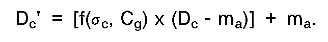
- Circuitry for determinating the enhanced or modified value, D c ', for the center pixel of the scanning window in accordance with the following equation where n is an integer of 0 or greater which is in accordance with the form for the unsharp masking filter equation (2.2).
- D c [g x (D c - m a )] + m a
- a further aspect of the present invention is the further utilization of the annular mean, m a , for use in determining the local background which is usable when it is desired that the enhanced or modified data signal for a pixel be used for printing on a bi-level basis, i.e., a mark or no mark.
- a predication can be made of the threshold to be used for making a comparison with the value of the enhanced pixel signal to determine whether a mark is to be made. If the enhanced pixel value is determined to be greater than the threshold, such pixel value will be used to produce a mark when a positive image is to be produced or not produce a mark when a negative image is desired.
- An estimate of the background, relative to the pixel for which an enhanced or modified pixel value has been determined, is made using the average of the annular mean values for the modified pixel and for windows centered on a pixel that is a fixed number of consecutive pixels ahead of and behind the modified pixel.
- An alternative approach uses the average of annular mean values for a fixed number of windows ahead of and behind the pixel in question wherein such windows do not overlap. Both approaches use annular mean values which are close enough to the pixel in question and yet spread far enough apart to provide a valid estimation of the local background.
- Threshold values that are to be used are available in a look-up table provided in a memory. The background value is used with a contrast control value to select the threshold value that is to be used from the look-up table.
- This threshold value and the value of the enhanced pixel are presented to a comparator for determining whether the enhanced pixel exceeds the threshold.
- the output of the comparator is directed for use by whatever type of device or apparatus is used to produce an image or may be placed in memory for use at a later time.
- An enhanced pixel value that exceeds the threshold will be used to cause a mark to be produced by the imaging device or apparatus and not cause a mark to be produced when the threshold is not exceeded in the case of positive images.
- Each enhanced pixel value, D c ′ is usable to produce an image mark wherein the pixel value determines the density of the image
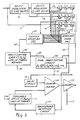
- the circuit used to produce the enhanced pixel value, D c ′ includes shift registers 12 and 14, a window shift register 16, annular mean circuit portion 18, center deviation circuit portion 20, modification gain, f( ⁇ c , C g ) look-up tables memory 22 and a pixel modification circuit portion 24.
- the image pixel values in digitized form, 8-bits for each pixel, for example, are serially supplied to the input 6 of window shift register 16 and to the shift register 12, which has a capacity to store one line of the image to provide a delay of one line. Such delay can also be provided by use of an addressable random access memory.
- the output of the shift register 12 is supplied to the input 8 of window shift register 16 and to shift register 14 which also provides a delay of one line.
- the output of shift register 14 is supplied to the input 13 of window shift register 16. Referring to the window shift register 16, a pixel value supplied to the input 13 appears at location D1, is then shifted to location D2 and then to location D3 as the shift register 16 is clocked.
- a pixel value supplied to the input 8 of register 16 appears at location D4, then D c and then location D5.
- a similar receipt and shifting of a pixel value received at input 6 occurs with respect to locations D6, D7 and D8. Accordingly, with each clock signal a new set of pixel values are presented to make up a window.
- Each of the locations D1-D8 have an output which is connected to the annular means circuit portion 18 and the center deviation circuit portion 20.
- the center pixel location D c of the window shift register 16 has an output 54 for supplying the center pixel value, D c , to the pixel modification circuit portion 24 and to the center deviation circuit portion 20.
- the annular mean (m a ) is calculated by the circuit portion 18 for the window 16 that is provided for each center pixel, D c , that is presented with result at output 53 being provided to the pixel modification circuit portion 24.
- the annular mean is the average value of 2 N pixels of the pixel window 16, where N is 1 or greater, which surround a given center pixel without using the value of the center pixel. In the arrangement shown in Figure 1, all eight pixels surrounding the center pixel of window 16 are used so the annular mean calculation requires a division by eight, after the sum of the eight pixel values D1-D4 and D5-D8 are obtained.
- Another way which can be readily implemented for a window of the invention, involves adding the pixel values surrounding the center pixel in pairs, dividing the pair sums by two, adding the results by pairs, dividing such sums by two, and repeating such process until a single sum is obtained and again dividing by two.
- Each division by two is easily accomplished since the result of a division by two only requires that the least significant bit in the binary output not be used. While a small error is introduced, it is not significant.
- groups of four of the pixel values surrounding the center pixel that are to be used can be added with the sum divided by four by not using the least and next significant bit in the binary output.
- D1 and D2 pixel values are added at adder 25, D2 and D4 at adder 26, D5 and D6 at adder 27 and D7 and D8 at adder 28 with a division by two carried out at the output of the adders 25-28 by not using the least significant bit (LSB) output when applying the output of adders 25 and 26 to an adder 29 and when applying the output of adders 27 and 28 to an adder 30.
- a division by two is similarly carried out at the output of adders 29 and 30 with the results being applied to adder 31 where a division by two is again carried out at the output 53 of adder 31 to provide the desired annular mean, m a , value for the window.
- all adders 25-31 are identical and are of minimum size and complexity. Further, it should be noted that all pixel values are processed in the same manner so that none of the pixel values are weighted disproportionately.
- a selected number of the pixel values surrounding the center pixel of a pixel window are provided for calculation of the center deviation at the circuit portion 20.
- all of the pixel values, D1-D8 and D c , for the 3 X 3 window 16 of Figure 1 are provided to the center deviation circuit portion 20 where the center deviation, ⁇ c , for the window 16 for each center pixel, D c , that is present is determined.
- the center deviation, ⁇ c is the sum of the absolute value of the differences between the center pixel and the selected surrounding pixels for a window. In the case of a 3 x 3 window, such as window 16, all pixels surrounding the center pixel are used. This involves the determination of eight differences which are summed.
- Figure 3 shows an exemplary circuit 20 for implementation of the calculation of the center deviation, ⁇ c , as set forth in equation (7.1).
- Eight binary subtractor circuits 32-39 are used to provide the absolute differences between the center pixel, D c , and each of the surrounding pixels, D1-D8, for the 3 x 3 window 16.
- each single line represents eight input lines, one for each of the 8-bits used for the pixel values.
- one input for each of the subtractors 32-39 is used for receiving the value of the center pixel, D c , with subtractors 32-39 also receiving the values for pixels, D1-D8, respectively.
- adder 40 sums the output from subtractors 32 and 33
- adder 41 sums the output from subtractors 34 and 35
- adder 42 sums the output from subtractors 36 and 37 with adder 43 summing the output from subtractors 38 and 39.
- the output line for each of the adders 40-43 represents nine output lines.
- the sum provided at the output of adders 40 and 41 provides the input to adder 44 while the sum provided at the output of adders 42 and 43 provides the input to adder 45.
- the sum provided by ten output lines from adders 44 and 45 is applied to adder 46 for summing.
- the output 47 of adder 46 which requires eleven output lines, provides the center deviation, ⁇ c , signal.
- the center deviation, ⁇ c , determined at 47 by the center deviation circuit 20 is used in a determination of the amount of modification or enhancement that is to be applied to the center pixel D c .
- the center deviation, along with a gain control input 50, is used as the address for the look-up tables memory 22 that contains previously calculated values of the gain control. Compilation of the look-up tables takes into consideration the number of absolute differences obtained in the calculation of the center deviation. If this is not done, the center deviation determined at the circuit portion 20 is divided by such number to provide a center deviation mean.
- Such division to provide the center deviation means can be readily carried out by modifying circuitry of the form of Figure 3 to obtain an output from adder 46 which only includes the output lines that are more significant than the output line having the most significant bit for the number of absolute differences that are obtained by such circuitry.
- Another possible modification, which would provide the center deviation means would eliminate use of the least significant output line for the output of the adders 41-46 of Figure 3, which for Figure 3 would provide an output at the adder 46 that is equal to the sum of the differences provided by the subtractors 32-39 divided by the number of the subtractors, i.e., eight. If a division is not carried out for a determination of the center deviation, the resolution in f( ⁇ ,C g ) is increased.
- the gain control obtained from the look-up tables is applied to the circuit portion 24 which provides for a calculation of the modified or enhanced center value pixel value, D c ′, in accordance with equation (6.1).
- the circuit portion 24 is shown in greater detail in Figure 4 and includes a subtractor circuit 52 to which the annular mean, m a , at 53 is provided along with the center pixel value, D c , at 54 to subtract the annular mean, m a , from the center pixel value, D c .
- a multiply circuit 55 is also provided to which the output 56 of the subtractor 52 (including the sign bit) is applied along with the gain control value, f( ⁇ c ,C g ), supplied at 57 from the look-up tables memory 22 to provide the product of multiplying the gain control value, f( ⁇ c ,C g ) and the output, (D c -m a ), from the subtractor 52 which product is supplied at 58 to an adder 59 along with the annular mean, m a , provided at 53 to provide the enhanced or modified center pixel value, D c ′, at its output 10.
- the enhanced or modified center pixel values presented at the output 10 of the pixel modification circuit 24 are useful for making an image where the process produces gray level images which are defined by the eight bit level signal for each pixel.
- the digitally defined pixel can be used to provide an image on a bi-level basis, i.e., mark or no mark.
- a useful measurement of the local background can be made by using the annular mean value that is determined by the annular mean circuit portion 18, for the center pixels of the pixel windows.
- the annular mean values that are used must be close enough to the pixel in question and yet spread far enough apart.
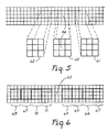
- FIG. 5 One such arrangement is schematically illustrated in Figure 5 wherein three 3 X 3 windows are used, the window 60 having the center pixel 48 for which an enhanced value has been determined and is to be compared with a threshold value, a window 61 that is centered on a pixel that is five pixels ahead of the center pixel of window 60 and a window 62 that is centered on a pixel that is five pixels behind the pixel that is the center pixel of window 60.
- the average of the annular means determined for each of these three windows is usable as a measure of the background relative to the center pixel of window 60.
- FIG. 6 Another arrangement that can be readily implemented with circuitry using the annular means for eight windows is schematically illustrated in Figure 6.
- the annular means for four 3 X 3 non-overlapping windows 64-67 ahead of pixel 63 is used along with the annular means for four 3 X 3 non-overlapping windows 68-71 behind the pixel 63.
- the average of the annular means for the eight non-overlapping windows 64-71 is determined and used as the background value for the pixel 63.
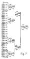
- Circuitry implementing the arrangement described in connection with Figure 6 is shown in Figure 7.
- Figure 6 for the eight annular means for windows 64-71 to be available for averaging, twenty-four series connected shift registers 172-195 are used.
- Four adder circuits 96-99 each having two inputs for eight bit signals, are used to receive the annular mean for the windows 64-71.
- the input 68a of adder 96 receives the annular means for window 68 which is also presented to the shift register 172. This occurs when the input 67a for adder 99 is receiving the annular mean for window 67.
- the other input 69a for adder 96 which is connected to the output of shift register 174, is then receiving the annular mean for window 69.
- the annular mean for window 70 is then presented at the output of shift register 177 which is connected to the input 70a of adder 97.
- the other input 71a for adder 97 which is connected to the output of shift register 180, then receives the annular mean for window 71.
- the annular mean for window 64 is then presented at the output of shift register 186 which is connected to the input 64a of adder 98.
- the other input 65a for adder 98 which is connected to the output of shift register 189, then receives the annular mean for window 65.
- the annular mean for window 66 is then presented at the output of shift register 192, which is connected to the input 66a of adder 99.
- the circuitry of Figure 7 also includes adders 100 and 101.
- the least significant bit output line of the nine line output of adder 96 is not connected to the input 102 of adder 100 so that the sum of the annular mean for windows 68 and 69 provided by adder 96 is divided by two and supplied to adder 100.
- the output of adder 97 is similarly connected to the other input 103 of adder 100.
- the outputs of adder 98 and adder 99 are connected to the inputs 104 and 105, respectively, of adder 101.
- An adder 106 is also included, which has its inputs 107 and 108 similarly connected to the output of adders 100 and 101, respectively.
- the output of adder 106 does not include the least significant bit of the sum of the two inputs causing the output to be the average of the eight annular means for windows 64-71.
- the portion of the circuitry that includes the adders 96-106 to obtain an average of eight inputs is similar in structure and function as the portion of the circuitry for Figure 2 wherein adders 25-31 are used to obtain the average of eight inputs
- circuitry for thresholding the enhanced pixel output 10 from the circuit portion 24 to permit its use for the production of an image on a bi-level bases includes a background detection circuit portion 110, a memory 111 of threshold value look-up tables, a comparator 112, a delay circuit 113, and an inverter 115.
- the background detection circuit portion 110 can take the form of the circuitry described in connection with Figure 7.
- the background detection circuit portion 110 receives the annular means, m a from the annular means circuit portion 18 to provide a background value for each enhanced pixel value obtained from the pixel modification circuitry.
- the background value is used as an address for the threshold value look-up table in memory 111 that is selected by a table selection input 116 to the memory 111.
- the threshold eight bit value obtained from memory 111 is applied to one eight bit input of the comparator 112 which receives each enhanced pixel value at its other eight bit input from the pixel modification circuit 24 via a delay circuit 113.
- the delay circuit 113 provides the delay necessary to have the pixel valued supplied to the comparator 112, at the time the background value is provided for such pixel value.
- the amount of delay provided by the delay circuit 113 is dependent on the manner in which the background value is determined at the background detection circuit 110 and also the method of obtaining D c ′.
- the comparator 112 will provide one output of one bit if the enhanced pixel value exceeds or is equal to the threshold value for the pixel value supplied to the comparator 112 and will provide a different output of one bit if the enhanced pixel value is less than such threshold value.
- the output of the comparator 112 is supplied to the inverter 115 which passes the output from the comparator 112 and or inverts it according to an output control 117 supplied to the inverter 115. If the output of the comparator 112 provided when the pixel value is greater than or equal to the threshold value is passed by the inverter 115, it can be used with an imaging process to produce a mark and if such output from the comparator 112 is inverted it will not produce a mark when used with an imaging progress.
- the inverter 115 passes the output of the comparator 112 that is provided when the enhanced pixel value is less than the threshold, it will not produce a mark when used with an imaging process. However, if such output from the comparator 112 is inverted by the inverter 115, it will produce a mark when used in an imaging process.
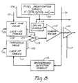
- Figure 8 shows a modification to the portion of Figure 1 just described.
- the modification allows the enhanced pixel value obtained from the circuit portion 24 to be used to make a one bit signal based on a halftone method, if desired.
- the modification includes the addition of a memory 118 and a multiplexer 119.
- the memory 118 has halftone value look-up tables. Selection of a halftone value is determined by a table selection input 120 for the memory 118 along with an address based on pixel and line counts supplied for an address input 121 for the memory 118.
- the multiplexer 119 receives the output at 122 from memory 111 and the output at 123 from memory 118.
- a control 124 is provided at the multiplexer 119 to select which of the inputs 122 and 123 from memories 111 and 118, respectively, will pass to one of the eight bit inputs to comparator 112.
- a 5 X 5 window can be used if the following pixel values are not applied to the annular mean 18: the first two and the last pixel value in row one; the last pixel value of row two; the first pixel value of row four and the first and last two pixel values of row five.
- a 7 X 7 pixel window is also usable if four pixel values in each corner of the window are not used to calculate the annular mean. With sixteen pixels not utilized, thirty-two (25) pixel values surrounding the center pixel are used to calculate the annular mean.
- a 13 X 13 pixel window is also usable. In this case, in the first and last row only pixel values at positions six and eight are used and in columns one and thirteen, only pixel values at positions six and eight are used. With this configuration, one hundred-twenty-eight (27) pixel values surrounding the center pixel are used to calculate the annular mean. As another example, a 17 X 17 pixel window is usable if eight pixels in each corner of the window are not used so that two hundred-fifty-six (28) pixel values surrounding the center pixel are used to calculate the annular mean.
- the eight pixel values not used for such corner be the first four of the first row; the first two of the second row and the first pixel in of rows three and four.
- the eight pixel values not used in the other three corners are selected to provide the same sort of configuration for such corners.
- a suitable pixel window need not have the same number of rows and columns. For example, a 5 X 7 pixel window is suitable if two pixels that are at opposite corners are not used for the annular means calculation so that thirty-two (25) pixel values surrounding the center pixel are used to calculate the annular mean.
- the foregoing examples illustrate how other still larger pixel windows could be used, if desired.
- the pixel value selected may be only those falling within a circle of a selected radius drawn on a representation of the pixel window with the center pixel as the center which may give a more accurate center deviation measurement for a particular pixel window.
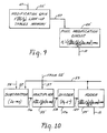
- any division done at pixel modification circuitry be by a number whereby the division can be readily accomplished, for example, division by 2 n , where n is an integer equal to 0 or more. "n" equal to three or four is preferred.
- Division by the pixel modification circuitry requires a change in the circuitry shown in Figure 1 and 4. The necessary changes are reflected in circuit portions 22′ and 24′ of Figure 10 which are used in place of circuit portions 22 and 24 of Figure 1.
- Circuit portion 22′ differs from portion 22 in that the look-up table values are different.
- the modification gain in portion 22′ is indicated as f′( ⁇ c ,C g ) rather than f( ⁇ c ,C g ) as indicated in portion 22 of Figure 1.
- Circuit portion 24′ of Figure 10 differs from circuit portion 24 of Figure 1 in that the equation for the output of portion 24′ shows a division by 2 n so that Referring to Figure 10, it differs from Figure 4 in that the multiplier 55′ reflects a multiplication of f′( ⁇ c ,C g ) x (D c -m a ) rather than a multiplication of f( ⁇ c ,C g ) x (D c -m a ) as shown for the multiplier 55 of Figure 1.
- the output 58 of multiplier 55′ is applied to a divider 126, where the result obtained from multiplier 55′ is divided by 2 n , n being an integer equal to 0 or greater with 3 or 4 preferred.
- adder 59′ of Figure 10 receives the output 127 of adder 126 as an input rather than having an input from a multiplier circuit as in Figure 1.
- the output 10 from adder 59′ which also receives the value of m a via 53, is the value for D c ′ as reflected by the equation shown in 59′ which corresponds to the equation shown in block 24′ of Figure 10.
- the annular mean, m a for a center pixel, D c , has application for the modification of such pixel without being limited to the particular manner in which the gain modification is obtained from the center pixel D c and selected pixels of the pixel window.
Landscapes
- Physics & Mathematics (AREA)
- General Physics & Mathematics (AREA)
- Engineering & Computer Science (AREA)
- Theoretical Computer Science (AREA)
- Facsimile Image Signal Circuits (AREA)
- Image Processing (AREA)
- Picture Signal Circuits (AREA)
Claims (15)
- System zur Modifizierung der dem System zugeführten Pixel, bei denen es sich um Mehrpegelsignale für ein digitalisiertes Bild handelt, wobei:
eine Einrichtung (6, 12, 14) aus den dem System zugeführten Pixeln ein Wanderpixelfenster (16) vorsieht, wobei das Pixelfenster ein Mittelpixel Dc und mindestens 2N Pixel umfaßt, welche das Mittelpixel umgeben, wobei N eine Integerzahl von größer oder gleich 1;
eine Einrichtung (18) 2N der das Mittelpixel umgebenden Pixel empfängt und für den Ringmittelwert ma der genannten emfangenen 2N Pixel sorgt; und wobei
eine Einrichtung (20, 22, 24) das Mittelpixel Dc empfängt sowie aus den das Mittelpixel umgebenden Pixeln ausgewählte Pixel des Pixelfensters (16), um eine Modifikationsverstärkung g vorzusehen und wobei die Einrichtung den Ringmittelwert ma empfängt, um gemaß der folgenden Gleichung ein modifiziertes Mittelpixel Dc' vorzusehen:

- System nach Anspruch 1, dadurch gekennzeichnet, daß die letztgenannte Einrichtung folgendes umfaßt:
eine Einrichtung (20), die das Mittelpixel und die aus dem das Mittelpixel umgebenden Pixelfenster ausgewählten Pixel empfängt, um für eine Ausgabe (47) zu sorgen, und zwar auf der Basis der Mittelabweichung σc für das Mittelpixel; und
eine Einrichtung (22), die mit der Ausgabe (47) verbunden ist, um eine Modifikationsverstärkung f(σc, Cg) als Modifikationsverstärkung g zu erhalten; und
eine Einrichtung (24), welche das Mittelpixel Dc, den Ringmittelwert ma und die Modifikationsverstärkung f(σc, Cg) empfängt, um gemäß der folgenden Gleichung ein modifiziertes Mittelpixel Dc' zu schaffen:

- System nach Anspruch 1, dadurch gekennzeichnet, daß die letztgenannte Einrichtung folgendes umfaßt:
eine Einrichtung (20), die das Mittelpixel und die aus dem das Mittelpixel umgebenden Pixelfenster ausgewählten Pixel empfängt, um für eine Ausgabe (47) zu sorgen, und zwar auf der Basis der Mittelabweichung σc für das Mittelpixel; und
eine Einrichtung (22'), die mit der Ausgabe (47) verbunden ist, um eine Modifikationsverstärkung f'(σc, Cg) als Modifikationsverstärkung g zu erhalten; und
eine Einrichtung (24'), welche das Mittelpixel Dc, den Ringmittelwert ma und die Modifikationsverstärkung f'(σc, Cg) empfängt, um gemäß der folgenden Gleichung ein modifiziertes Mittelpixel Dc' zu schaffen:
- System nach Anspruch 2 oder 3, dadurch gekennzeichnet, daß es sich bei der mit der Ausgabe (47) verbundenen Einrichtung (22, 22') um einen Speicher handelt, der Modifikationsverstärkungstabellen enthält.
- System nach Anspruch 2 oder 3, dadurch gekennzeichnet, daß die auf der Mittelabweichung basierende Ausgabe (47) gleich der Mittelabweichung geteilt durch die Anzahl der ausgewählten Pixel ist.
- System nach Anspruch 1, 2 oder 3, ferner mit:
einem Hintergrunderfassungskreisteil (110), der den Ringmittelwert empfängt, um eine Ausgabe zu liefern, die ein Maß des Hintergrunds für das modifizierte Mittelpixel darstellt;
einer Einrichtung (111), die zur Erzielung eines Schwellenwertes mit der Ausgabe des Hintergrunderfassungskreisteils (110) verbunden ist; und
einem Vergleicher (112), der den Schwellenwert an einem Eingang des Vergleichers empfängt und der das modifizierte Mittelpixel an einem zweiten Eingang des Vergleichers empfängt, für das ein Maß dessen Hintergrundes durch den Hintergrunderfassungskreis vorgesehen ist, wobei der Vergleicher (112) ein Ausgangssignal liefert, wenn das modifizierte Mittelpixel an dem zweiten Eingang den Schwellenwert an dem einen Eingang überschreitet oder diesem gleicht und der Vergleicher liefert ein anderes Ausgangssignal, wenn das modifizierte Mittelpixel unter dem Schwellenwert liegt. - System nach Anspruch 5, dadurch gekennzeichnet, daß die Einrichtung (111) zur Erzielung eines Schwellenwertes, einen Speicher darstellt, der Schwellenwerttabellen enthält.
- System nach Anspruch 1, 2 oder 3, ferner mit:
einem Speicher (118), der Tabellen von Halbtonwerten enthält; und
einem Vergleicher (112) zum Empfang eines Halbtonwerts von dem Speicher an dem einen Eingang des Vergleichers des modifizierten Mittelpixels an einem zweiten Eingang des Vergleichers, wobei der Vergleicher ein Ausgangssignal liefert, wenn das modifizierte Mittelpixel an dem Eingang den Halbtonwert an dem einen Eingang übersteigt oder diesem gleicht und wobei der Vergleicher ein anderes Ausgangssignal liefert, wenn das modifizierte Mittelpixel unter dem Kalbtonwert an dem einen Eingang liegt. - Verfahren zur Modifizierung von Pixeln, die Mehrpegelsignale für ein digitalisiertes Bild darstellen, umfassend die Schritte:(a) Begründung eines Wanderpixelfensters aus den Pixeln, wobei das Pixelfenster ein Mittelpixel Dc aufweist und mindestens 2N Pixel, die das Mittelpixel umgeben, wobei N eine Integerzahl von größder oder gleich 1 darstellt;(b) Bestimmung des Ringmittelwerts ma von 2N Pixeln, der das Mittelpixel für jedes begründete Pixelfenster umgebenden Pixel;(c) Begründung einer Modifikationsverstärkung g für jedes Mittelpixel; und(d) Verarbeitung des Ringmittelwerts ma, des Mittelpixels Dc und der Modifikationsverstärkung g, um so gemäß der folgenden Gleichung ein modifiziertes Mittelpixel Dc' zu erzeugen:

- Verfahren zur Modifizierung von Pixeln, die Mehrpegelsignale für ein digitalisiertes Bild darstellen, nach Anspruch 9, wobei ein Schritt enthalten ist, bei dem die Mittelabweichung für das Mittelpixel jedes begründeten Fensters, unter Verwendung ausgewählter, das Mittelpixel umgebender Pixel, bestimmt wird und wobei der Schritt der Bereitstellung einer Modifikationsverstärkung g für jedes Mittelpixel eine Modifikationsverstärkung f(σ, Cg) für jedes Mittelpixel vorsieht, die auf der Mittelabweichung basiert und welche bei der Anwendung bei der Verarbeitung des letzten Schritts ein modifiziertes Mittelpixel Dc' zur Folge hat, und zwar gemäß der folgenden Gleichung:
- Verfahren zur Modifizierung von Pixeln, die Mehrpegelsignale für ein digitalisiertes Bild darstellen, nach Anspruch 9, wobei ein Schritt enthalten ist, bei dem die Mittelabweichung für das Mittelpixel jedes begründeten Fensters, unter Verwendung ausgewählter, das Mittelpixel umgebender Pixel, bestimmt wird und wobei der Schritt der Bereitstellung einer Modifikationsverstärkung g für jedes Mittelpixel eine Modifikationsverstärkung f'(σc, Cg) für jedes Mittelpixel vorsieht, die auf der Mittelabweichung basiert und welche bei der Anwendung bei der Verarbeitung des letzten Schritts ein modifiziertes Mittelpixel Dc' zur Folge hat, und zwar gemäß der folgenden Gleichung:

- Verfahren zur Modifizierung von Pixeln, die Mehrpegelsignale für ein digitalisiertes Bild darstellen, nach Anspruch 10 oder 11, wobei der Schritt der Begründung der Modifikationsverstärkung die Bereitstellung eines Speichers umfaßt, der Modifikationsverstärkungstabellen enthält und der die Mittelabweichung zum Zugriff auf den Speicher verwendet, um die Modifikationsverstärkung zu begründen.
- Verfahren zur Modifizierung von Pixeln, die Mehrpegelsignale für ein digitalisiertes Bild darstellen, nach Anspruch 10, 11 oder 12, umfassend die zusätzlichen Schritte:
der Verwendung des Ringmittelwertes ma zur Bereitstellung eines Maßes des Hintergrunds für das modifizierte Mittelpixel;
der Begründung eines Schwellenwertes, basierend auf dem Maß des Hintergrunds;
des Vergleichs des genannten Schwellenwertes mit dem modifizierten Pixel und Bereitstellung eines Signals, wenn das modifizierte Pixel größer oder gleich dem Schwellenwert ist und Bereitstellung eines anderen Signals, wenn das modifizierte Pixel unter dem Schwellenwert liegt. - Verfahren zur Modifizierung von Pixeln, die Mehrpegelsignale für ein digitalisiertes Bild darstellen, nach Anspruch 13, wobei der Schritt der Begründung eines Schwellenwerts die Bereitstellung eines Speichers umfaßt, der Schwellenwerttabellen enthält und Verwendung des Maßes des Hintergrunds zum Zugriff auf den Speicher zur Begründung des Schwellenwerts.
- Verfahren zur Modifizierung von Pixeln, die Mehrpegelsignale für ein digitalisiertes Bild darstellen, nach Anspruch 9, 10, 11 oder 12, umfassend die zusätzlichen Schritt:
der Bereitstellung eines Speichers, der Halbtonwerttabellen enthält; und
den Vergleich eines aus dem Speicher erhaltenen Halbtonwerts und Bereitstellung eines Signals, wenn das modifizierte Pixel größer oder gleich dem Halbtonwert ist und Bereitstellung eines anderen Signals, wenn das modifizierte Pixel unter dem Halbtonwert liegt.
Applications Claiming Priority (2)
| Application Number | Priority Date | Filing Date | Title |
|---|---|---|---|
| US219377 | 1988-07-15 | ||
| US07/219,377 US4941190A (en) | 1988-07-15 | 1988-07-15 | Method and system for enhancement of a digitized image |
Publications (3)
| Publication Number | Publication Date |
|---|---|
| EP0352016A2 EP0352016A2 (de) | 1990-01-24 |
| EP0352016A3 EP0352016A3 (de) | 1991-05-22 |
| EP0352016B1 true EP0352016B1 (de) | 1994-03-30 |
Family
ID=22819033
Family Applications (1)
| Application Number | Title | Priority Date | Filing Date |
|---|---|---|---|
| EP89307093A Expired - Lifetime EP0352016B1 (de) | 1988-07-15 | 1989-07-13 | Verfahren und System zur Verbesserung eines digitalisierten Bildes |
Country Status (6)
| Country | Link |
|---|---|
| US (1) | US4941190A (de) |
| EP (1) | EP0352016B1 (de) |
| JP (1) | JPH0273477A (de) |
| CA (1) | CA1309502C (de) |
| DE (1) | DE68914206T2 (de) |
| IL (1) | IL90654A (de) |
Families Citing this family (75)
| Publication number | Priority date | Publication date | Assignee | Title |
|---|---|---|---|---|
| JPH0690724B2 (ja) * | 1988-07-29 | 1994-11-14 | 大日本スクリーン製造株式会社 | 画像の輪郭強調方法 |
| US5038388A (en) * | 1989-05-15 | 1991-08-06 | Polaroid Corporation | Method for adaptively sharpening electronic images |
| JP2650759B2 (ja) * | 1989-07-21 | 1997-09-03 | 富士写真フイルム株式会社 | 画像処理装置 |
| US5216521A (en) * | 1990-01-10 | 1993-06-01 | Agfa-Gevaert Aktiengesellschaft | Reproduction of photographic originals with scattered light correction |
| JPH03245675A (ja) * | 1990-02-23 | 1991-11-01 | Matsushita Electric Ind Co Ltd | 画像処理装置 |
| JP2574923B2 (ja) * | 1990-04-10 | 1997-01-22 | 大日本スクリーン製造株式会社 | 輪郭強調方法および画像処理装置 |
| US5506917A (en) * | 1990-07-13 | 1996-04-09 | Nippon Telegraph And Telephone Corporation | Thresholding method for segmenting gray scale image, method for determining background concentration distribution, and image displacement detection method |
| US5268860A (en) * | 1990-09-17 | 1993-12-07 | Victor Company Of Japan, Ltd. | Image enhancement system |
| US5271064A (en) * | 1991-06-14 | 1993-12-14 | University Of Cincinnati | Apparatus and method for smoothing regions and enhancing edges in gray scale images |
| US5237402A (en) * | 1991-07-30 | 1993-08-17 | Polaroid Corporation | Digital image processing circuitry |
| US5381241A (en) * | 1991-08-13 | 1995-01-10 | Sharp Corporation | Method for discriminating between figure and text areas of an image |
| EP0531904A3 (en) * | 1991-09-10 | 1993-10-06 | Eastman Kodak Company | Method and apparatus for spatially variant filtering |
| JP3366633B2 (ja) * | 1991-11-27 | 2003-01-14 | セイコーエプソン株式会社 | ピクセル変更システム及びピクセル変更方法 |
| JP3092024B2 (ja) * | 1991-12-09 | 2000-09-25 | 松下電器産業株式会社 | 画像処理方法 |
| US5239390A (en) * | 1992-06-05 | 1993-08-24 | Eastman Kodak Company | Image processing method to remove halftone screens |
| US5341174A (en) * | 1992-08-17 | 1994-08-23 | Wright State University | Motion compensated resolution conversion system |
| US5524070A (en) * | 1992-10-07 | 1996-06-04 | The Research Foundation Of State University Of New York | Local adaptive contrast enhancement |
| IT1258122B (it) * | 1992-11-25 | 1996-02-20 | Seleco Spa | Sistema migliorativo del contrasto di immagini video utilizzante un filtro di volterra del secondo ordine. |
| US5710840A (en) * | 1993-04-26 | 1998-01-20 | Fuji Photo Film Co., Ltd. | Image processing method and apparatus for adjusting the tone density of pixels based upon differences between the tone density of a center pixel and tone densities of peripheral pixels |
| CA2128389C (en) * | 1993-10-15 | 1999-05-11 | Lawrence Patrick O'gorman | Method of reducing document size for digital display |
| JP2856661B2 (ja) * | 1993-11-05 | 1999-02-10 | シャープ株式会社 | 濃度変換装置 |
| JPH07248557A (ja) * | 1994-03-10 | 1995-09-26 | Konica Corp | 放射線画像の処理方法 |
| JP3547481B2 (ja) * | 1994-04-19 | 2004-07-28 | 松下電器産業株式会社 | 映像信号処理方法および映像信号処理装置 |
| WO1995030208A2 (en) * | 1994-05-03 | 1995-11-09 | Philips Electronics N.V. | Better contrast/noise by residue image |
| US5812691A (en) * | 1995-02-24 | 1998-09-22 | Udupa; Jayaram K. | Extraction of fuzzy object information in multidimensional images for quantifying MS lesions of the brain |
| US5933540A (en) * | 1995-05-11 | 1999-08-03 | General Electric Company | Filter system and method for efficiently suppressing noise and improving edge definition in a digitized image |
| FR2737034A1 (fr) * | 1995-07-21 | 1997-01-24 | Philips Electronique Lab | Procede de traitement spatial d'une image numerique pour la reduction du bruit, et dispositif mettant en oeuvre ce procede |
| US5903681A (en) * | 1996-07-24 | 1999-05-11 | Eastman Kodak Company | Reducing edge artifacts on a digital printer |
| US5982941A (en) * | 1997-02-07 | 1999-11-09 | Eastman Kodak Company | Method of producing digital image with improved performance characteristic |
| US6069979A (en) * | 1997-02-25 | 2000-05-30 | Eastman Kodak Company | Method for compressing the dynamic range of digital projection radiographic images |
| US5978518A (en) * | 1997-02-25 | 1999-11-02 | Eastman Kodak Company | Image enhancement in digital image processing |
| US6639945B2 (en) | 1997-03-14 | 2003-10-28 | Microsoft Corporation | Method and apparatus for implementing motion detection in video compression |
| US6173317B1 (en) | 1997-03-14 | 2001-01-09 | Microsoft Corporation | Streaming and displaying a video stream with synchronized annotations over a computer network |
| US5809105A (en) * | 1997-03-19 | 1998-09-15 | General Electric Company | Noise filter for digital x-ray imaging system |
| US6075926A (en) * | 1997-04-21 | 2000-06-13 | Hewlett-Packard Company | Computerized method for improving data resolution |
| US6281942B1 (en) * | 1997-08-11 | 2001-08-28 | Microsoft Corporation | Spatial and temporal filtering mechanism for digital motion video signals |
| JP2964321B2 (ja) * | 1997-09-01 | 1999-10-18 | ジーイー横河メディカルシステム株式会社 | 画像表示方法、画像表示装置および画像診断装置 |
| US6088065A (en) * | 1997-09-03 | 2000-07-11 | Victor Company Of Japan, Ltd. | Contour correction apparatus and method |
| US6546405B2 (en) | 1997-10-23 | 2003-04-08 | Microsoft Corporation | Annotating temporally-dimensioned multimedia content |
| US6628329B1 (en) | 1998-08-26 | 2003-09-30 | Eastman Kodak Company | Correction of position dependent blur in a digital image |
| US6614474B1 (en) * | 1998-08-27 | 2003-09-02 | Polycom, Inc. | Electronic pan tilt zoom video camera with adaptive edge sharpening filter |
| US6424730B1 (en) | 1998-11-03 | 2002-07-23 | Eastman Kodak Company | Medical image enhancement method for hardcopy prints |
| US6195467B1 (en) * | 1999-03-25 | 2001-02-27 | Image Processing Technologies, Inc. | Method and apparatus for sharpening a grayscale image |
| FR2803069B1 (fr) * | 1999-12-28 | 2002-12-13 | Ge Medical Syst Sa | Procede et systeme de compensation de l'epaisseur d'un organe |
| EP1134969A1 (de) * | 2000-03-13 | 2001-09-19 | Koninklijke Philips Electronics N.V. | Bildverbesserung |
| US6512523B1 (en) * | 2000-03-27 | 2003-01-28 | Intel Corporation | Accurate averaging of elements using integer averaging |
| US6601077B1 (en) * | 2000-03-31 | 2003-07-29 | Intel Corporation | DSP unit for multi-level global accumulation |
| DE10017083A1 (de) * | 2000-04-06 | 2001-10-11 | Cgk Comp Ges Konstanz Mbh | Verfahren und Vorrichtung zur Störungsunterdrückung bei der Bildverarbeitung |
| AU2001279304A1 (en) | 2000-07-13 | 2002-01-30 | Christopher J. Feola | System and method for associating historical information with sensory data and distribution thereof |
| EP1239415A1 (de) * | 2001-03-05 | 2002-09-11 | Ge Medical Systems Sa | Verfahren und System zur Manipulation der Dynamik eines digitalen radiologischen Bildes |
| US7050086B2 (en) * | 2001-06-26 | 2006-05-23 | Pentax Corporation | Electronic endoscope system with color-balance alteration process |
| US6822657B2 (en) * | 2001-08-10 | 2004-11-23 | Agilent Technologies, Inc. | Method and apparatus for improving image quality in digital cameras |
| WO2003025912A1 (en) | 2001-09-17 | 2003-03-27 | Thomson Licensing, S.A. | Digital reproduction of optical film soundtracks |
| US7558816B2 (en) * | 2001-11-21 | 2009-07-07 | Sun Microsystems, Inc. | Methods and apparatus for performing pixel average operations |
| US20050029352A1 (en) * | 2003-08-08 | 2005-02-10 | Spears Kurt E. | System and method for automatic correction of illumination noise caused by ambient light |
| US20050052468A1 (en) * | 2003-09-05 | 2005-03-10 | Xerox Corporation. | Method of detecting half-toned uniform areas in bit-map |
| US20050105819A1 (en) * | 2003-11-13 | 2005-05-19 | Microsoft Corporation | Quick blur approximation |
| KR20050049062A (ko) * | 2003-11-21 | 2005-05-25 | 삼성전자주식회사 | 선명도 향상장치 및 그 방법 |
| US7143495B2 (en) * | 2004-03-05 | 2006-12-05 | Wing Brandon M | Backlight etching process |
| TW200606555A (en) * | 2004-08-11 | 2006-02-16 | ke-cong Li | Method for enhancing images of non-uniform brightness and electronic apparatus thereof |
| US8379988B1 (en) | 2008-03-04 | 2013-02-19 | Marvell International Ltd. | Image processing using stability criteria for pixel windows |
| US7734089B2 (en) * | 2005-08-23 | 2010-06-08 | Trident Microsystems (Far East) Ltd. | Method for reducing mosquito noise |
| KR100679047B1 (ko) * | 2005-09-29 | 2007-02-05 | 삼성전자주식회사 | 비트 해상도 확장 방법 및 장치 |
| US20070086650A1 (en) * | 2005-10-06 | 2007-04-19 | Keh-Tsong Li | Method and Device for Color Saturation and Sharpness Enhancement |
| JP4523926B2 (ja) * | 2006-04-05 | 2010-08-11 | 富士通株式会社 | 画像処理装置、画像処理プログラムおよび画像処理方法 |
| US7847979B2 (en) * | 2006-07-07 | 2010-12-07 | Eastman Kodak Company | Printer having differential filtering smear correction |
| US8351735B2 (en) | 2006-10-18 | 2013-01-08 | Robert Bosch Gmbh | Image processing system, method and computer program for contrast enhancement of images |
| US8228561B2 (en) * | 2007-03-30 | 2012-07-24 | Xerox Corporation | Method and system for selective bitmap edge smoothing |
| US7961972B2 (en) * | 2007-05-01 | 2011-06-14 | Intel Corporation | Method and apparatus for short range motion adaptive noise reduction |
| JP2008309296A (ja) * | 2007-06-18 | 2008-12-25 | Nitta Moore Co | 加熱・保温チューブ |
| US8368959B2 (en) | 2009-05-18 | 2013-02-05 | Xerox Corporation | Method and system for selective smoothing of halftoned objects using bitmap encoding |
| US8483609B2 (en) * | 2009-07-08 | 2013-07-09 | Viasat, Inc. | Interference resistant satellite link power control using uplink noise measurements |
| US8385223B2 (en) * | 2009-07-08 | 2013-02-26 | Viasat, Inc. | Interference resistant satellite link power control using downlink beacon |
| EP2564373B1 (de) * | 2010-04-26 | 2014-12-17 | Robert Bosch GmbH | Detektion und/oder erhöhung von kontrastunterschieden in digitalen bilddaten |
| DE102011055269A1 (de) * | 2011-11-11 | 2013-05-16 | Jenoptik Robot Gmbh | Verfahren zur Durchführung einer Dynamikkompression in der Verkehrsfotografie |
Family Cites Families (13)
| Publication number | Priority date | Publication date | Assignee | Title |
|---|---|---|---|---|
| JPS5533348A (en) * | 1978-08-31 | 1980-03-08 | Fuji Xerox Co Ltd | Noise elimination system |
| US4334244A (en) * | 1980-07-28 | 1982-06-08 | Magnavox Government And Industrial Electronics Company | Adaptive image enhancement system |
| US4504864A (en) * | 1982-12-30 | 1985-03-12 | International Business Machines Corporation | Nonlinear filtering of gray scale images |
| CH672212A5 (de) * | 1983-06-03 | 1989-10-31 | Gravure Inc | |
| US4571635A (en) * | 1984-02-17 | 1986-02-18 | Minnesota Mining And Manufacturing Company | Method of image enhancement by raster scanning |
| JPS60218181A (ja) * | 1984-04-13 | 1985-10-31 | Fujitsu Ltd | 画像処理装置 |
| DE3520405A1 (de) * | 1984-06-09 | 1985-12-12 | Fuji Photo Film Co., Ltd., Minami-Ashigara, Kanagawa | Verfahren zur bearbeitung von bildsignalen |
| US4794531A (en) * | 1984-11-07 | 1988-12-27 | Hitachi, Ltd | Unsharp masking for image enhancement |
| JPS61170178A (ja) * | 1985-01-24 | 1986-07-31 | Fuji Photo Film Co Ltd | 放射線画像情報の読取条件決定方法 |
| JPS61230571A (ja) * | 1985-04-05 | 1986-10-14 | Dainippon Screen Mfg Co Ltd | 画像走査装置 |
| JPS61285867A (ja) * | 1985-06-12 | 1986-12-16 | Dainippon Screen Mfg Co Ltd | 網点画像記録方法並びに装置 |
| DE3629409C2 (de) * | 1986-08-29 | 1994-02-17 | Agfa Gevaert Ag | Verfahren und Vorrichtung zur Kontrastbewertung bei der elektronischen Bildverarbeitung |
| JPS63158970A (ja) * | 1986-12-23 | 1988-07-01 | Matsushita Electric Ind Co Ltd | 画像読み取り装置 |
-
1988
- 1988-07-15 US US07/219,377 patent/US4941190A/en not_active Expired - Lifetime
-
1989
- 1989-06-19 IL IL90654A patent/IL90654A/xx not_active IP Right Cessation
- 1989-06-23 CA CA000603719A patent/CA1309502C/en not_active Expired - Lifetime
- 1989-07-13 EP EP89307093A patent/EP0352016B1/de not_active Expired - Lifetime
- 1989-07-13 DE DE68914206T patent/DE68914206T2/de not_active Expired - Fee Related
- 1989-07-14 JP JP1182398A patent/JPH0273477A/ja active Pending
Also Published As
| Publication number | Publication date |
|---|---|
| EP0352016A2 (de) | 1990-01-24 |
| US4941190A (en) | 1990-07-10 |
| JPH0273477A (ja) | 1990-03-13 |
| CA1309502C (en) | 1992-10-27 |
| DE68914206D1 (de) | 1994-05-05 |
| DE68914206T2 (de) | 1994-10-06 |
| IL90654A0 (en) | 1990-01-18 |
| EP0352016A3 (de) | 1991-05-22 |
| IL90654A (en) | 1992-06-21 |
Similar Documents
| Publication | Publication Date | Title |
|---|---|---|
| EP0352016B1 (de) | Verfahren und System zur Verbesserung eines digitalisierten Bildes | |
| US5666443A (en) | Image processor with edge emphasis of image data | |
| US6807300B1 (en) | Noise reduction method utilizing color information, apparatus, and program for digital image processing | |
| KR0173456B1 (ko) | 디더 처리방법 | |
| EP0031247B1 (de) | Vorrichtung und Verfahren zur Herstellung eines aus Streupunkten bestehenden Halbtonbildes aus einem Normalbild | |
| EP0407213B1 (de) | Bildverarbeitungsgerät | |
| EP0555674A2 (de) | System zur Bildherstellung und zugeordnetes Verfahren zur Minimierung von Konturen für ein quantisiertes Digitalfarbbild | |
| JP3238392B2 (ja) | 画像処理方法 | |
| US6891977B2 (en) | Method for sharpening a digital image without amplifying noise | |
| JPS62216476A (ja) | 画像処理装置 | |
| US6947176B1 (en) | Method for correcting lightness of image | |
| JPH05225332A (ja) | 空間的可変濾波の方法及び装置 | |
| US4682301A (en) | Digital filter for processing two-dimensional digital image | |
| EP0368162A2 (de) | Verfahren und Vorrichtung zur Verbesserung von Einzelheiten | |
| US5949915A (en) | Image processing method and apparatus | |
| Chaudhry et al. | Underwater visibility restoration using dehazing, contrast enhancement and filtering | |
| EP0579177B1 (de) | Farbbildverarbeitungsgerät | |
| JP2533652B2 (ja) | 画像輪郭処理方法 | |
| JP3118868B2 (ja) | 画像処理装置 | |
| JP2916171B2 (ja) | 画像処理装置 | |
| EP0992942A1 (de) | Verfahren zur Glättung des Stuffen-Effektes in Bildern geringer Auflösung | |
| JP3222570B2 (ja) | 像域識別装置 | |
| JPH10210298A (ja) | 画像処理方法及び装置 | |
| JPH065879B2 (ja) | 画像処理装置 | |
| JP3146518B2 (ja) | 画像処理装置 |
Legal Events
| Date | Code | Title | Description |
|---|---|---|---|
| PUAI | Public reference made under article 153(3) epc to a published international application that has entered the european phase |
Free format text: ORIGINAL CODE: 0009012 |
|
| AK | Designated contracting states |
Kind code of ref document: A2 Designated state(s): DE FR GB NL |
|
| 17P | Request for examination filed |
Effective date: 19910102 |
|
| PUAL | Search report despatched |
Free format text: ORIGINAL CODE: 0009013 |
|
| AK | Designated contracting states |
Kind code of ref document: A3 Designated state(s): DE FR GB NL |
|
| 17Q | First examination report despatched |
Effective date: 19930813 |
|
| GRAA | (expected) grant |
Free format text: ORIGINAL CODE: 0009210 |
|
| AK | Designated contracting states |
Kind code of ref document: B1 Designated state(s): DE FR GB NL |
|
| REF | Corresponds to: |
Ref document number: 68914206 Country of ref document: DE Date of ref document: 19940505 |
|
| ET | Fr: translation filed | ||
| PLBE | No opposition filed within time limit |
Free format text: ORIGINAL CODE: 0009261 |
|
| STAA | Information on the status of an ep patent application or granted ep patent |
Free format text: STATUS: NO OPPOSITION FILED WITHIN TIME LIMIT |
|
| 26N | No opposition filed | ||
| PGFP | Annual fee paid to national office [announced via postgrant information from national office to epo] |
Ref country code: GB Payment date: 19970620 Year of fee payment: 9 |
|
| PGFP | Annual fee paid to national office [announced via postgrant information from national office to epo] |
Ref country code: NL Payment date: 19970625 Year of fee payment: 9 |
|
| PGFP | Annual fee paid to national office [announced via postgrant information from national office to epo] |
Ref country code: FR Payment date: 19970711 Year of fee payment: 9 |
|
| PGFP | Annual fee paid to national office [announced via postgrant information from national office to epo] |
Ref country code: DE Payment date: 19970729 Year of fee payment: 9 |
|
| PG25 | Lapsed in a contracting state [announced via postgrant information from national office to epo] |
Ref country code: GB Free format text: LAPSE BECAUSE OF NON-PAYMENT OF DUE FEES Effective date: 19980713 |
|
| PG25 | Lapsed in a contracting state [announced via postgrant information from national office to epo] |
Ref country code: NL Free format text: LAPSE BECAUSE OF NON-PAYMENT OF DUE FEES Effective date: 19990201 |
|
| GBPC | Gb: european patent ceased through non-payment of renewal fee |
Effective date: 19980713 |
|
| PG25 | Lapsed in a contracting state [announced via postgrant information from national office to epo] |
Ref country code: FR Free format text: LAPSE BECAUSE OF NON-PAYMENT OF DUE FEES Effective date: 19990331 |
|
| NLV4 | Nl: lapsed or anulled due to non-payment of the annual fee |
Effective date: 19990201 |
|
| PG25 | Lapsed in a contracting state [announced via postgrant information from national office to epo] |
Ref country code: DE Free format text: LAPSE BECAUSE OF NON-PAYMENT OF DUE FEES Effective date: 19990501 |
|
| REG | Reference to a national code |
Ref country code: FR Ref legal event code: ST |