EP0351819A2 - Standard-Zellen mit Flip-Flops - Google Patents
Standard-Zellen mit Flip-Flops Download PDFInfo
- Publication number
- EP0351819A2 EP0351819A2 EP89113243A EP89113243A EP0351819A2 EP 0351819 A2 EP0351819 A2 EP 0351819A2 EP 89113243 A EP89113243 A EP 89113243A EP 89113243 A EP89113243 A EP 89113243A EP 0351819 A2 EP0351819 A2 EP 0351819A2
- Authority
- EP
- European Patent Office
- Prior art keywords
- flip
- clock
- standard cells
- routing
- flop circuits
- Prior art date
- Legal status (The legal status is an assumption and is not a legal conclusion. Google has not performed a legal analysis and makes no representation as to the accuracy of the status listed.)
- Granted
Links
Images


Classifications
-
- H—ELECTRICITY
- H03—ELECTRONIC CIRCUITRY
- H03K—PULSE TECHNIQUE
- H03K19/00—Logic circuits, i.e. having at least two inputs acting on one output; Inverting circuits
- H03K19/02—Logic circuits, i.e. having at least two inputs acting on one output; Inverting circuits using specified components
- H03K19/173—Logic circuits, i.e. having at least two inputs acting on one output; Inverting circuits using specified components using elementary logic circuits as components
- H03K19/177—Logic circuits, i.e. having at least two inputs acting on one output; Inverting circuits using specified components using elementary logic circuits as components arranged in matrix form
-
- G—PHYSICS
- G11—INFORMATION STORAGE
- G11C—STATIC STORES
- G11C5/00—Details of stores covered by group G11C11/00
- G11C5/06—Arrangements for interconnecting storage elements electrically, e.g. by wiring
- G11C5/063—Voltage and signal distribution in integrated semi-conductor memory access lines, e.g. word-line, bit-line, cross-over resistance, propagation delay
-
- G—PHYSICS
- G11—INFORMATION STORAGE
- G11C—STATIC STORES
- G11C11/00—Digital stores characterised by the use of particular electric or magnetic storage elements; Storage elements therefor
- G11C11/21—Digital stores characterised by the use of particular electric or magnetic storage elements; Storage elements therefor using electric elements
- G11C11/34—Digital stores characterised by the use of particular electric or magnetic storage elements; Storage elements therefor using electric elements using semiconductor devices
- G11C11/40—Digital stores characterised by the use of particular electric or magnetic storage elements; Storage elements therefor using electric elements using semiconductor devices using transistors
- G11C11/41—Digital stores characterised by the use of particular electric or magnetic storage elements; Storage elements therefor using electric elements using semiconductor devices using transistors forming static cells with positive feedback, i.e. cells not needing refreshing or charge regeneration, e.g. bistable multivibrator or Schmitt trigger
Definitions
- the present invention relates to standard cells which is a type of semi-custom LSI and, more particularly, to such standard cells which includes flip-flop circuits.
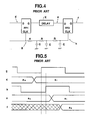
- a clock signal CLK1 for a first flip-flop FF1 and a clock signal CLK2 for a second flip-flop FF2 have, as shown in Fig. 2, a phase difference called skew due to presence of routing resistance R and routing capacitance C in a clock routing CLK between the first and second flip-flops FF1 and FF2.
- the appearance of such a skew in clock signal is called clock-skew. Since the longer routing makes more delay of a transmission of a clock signal between two flip flops, it is desirable for the flip-flops to have routing for clock signal as short as possible.
- the racing is avoided by providing an extra delay X between the output terminal Q of the first flip-flop FF1 and the input terminal D of the second flip-flop FF2, as shown in Fig. 4, such that a delay of data is suitably elongated to be compatible with a delay of clock due to the clock-skew so as to achieve a correct timing relationship shown in Fig. 5 in which the output in the routing f is correctly a0.
- a conventional standard cells has numbers of flip-flops F/F scattered in numbers of lines R as a result of designing, so that the clock routings l1, l2, l3, l4, and l5 become long and complicated, and neither an accurate estimation of the clock routing length nor minimization of the clock routing has been possible.
- standard cells comprising: substrate on which circuits are to be arranged; flip-flop circuits collectively arranged in a region of the substrate; clock routing for the flip-flop circuits with connections connecting the clock routing and each of the flip-flop circuits at shortest distance; and other circuits arranged in a remaining region of the substrate.
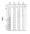
- Fig. 7 there is shown one embodiment of standard cells according to the present invention.
- standard cells is formed on an LSI substrate 10 by arranging numbers of flip-flops F/F collectively, one adjacent to another, all on a single cell line comprising a flip-flop area 12 which has an associated clock routing area 11 located nearby, along the flip-flop area 12, while other logical circuits are arranged in the remaining logical circuit area 13 with other routing area 14.
- the clock routings are arranged in very ordered and simple geometrical manner and, in particular, all the connections l1, l2, ⁇ , l n have the same length. All of these featuressignificantly contribute to the fact that in this embodiment the clock routing length can accurately be estimated. Thus, from the resistance and capacitance of the clock routing and the estimated clock routing length, it is possible to select an appropriate delay to be incorporated for an optimal protection against the racing.
- FIG. 7 there is shown another embodiment of standard cells according to the present invention.
- the previous embodiment is modified such that the flip-flops F/F are arranged not on a single cell line but on two cell lines.
- the same care to arrange the flip-flops F/F collectively in one specific region of the LSI substrate 10 has also been taken.
- the connections l1, l2, ⁇ , l i for an upper cell line for the flip-flops F/F and the connections l i+1 , ⁇ , 1 n for a lower cell line for the flip-flops separately have the same advantageous features of the connections l1, l2, ⁇ ,l n of the previous embodiment.
- the similar effects and advantages of the previous embodiment can be achieved by this embodiment.
- the clock routing may be incorporated within the flip-flop area 12, without providing a separate clock routing area 11.
Landscapes
- Engineering & Computer Science (AREA)
- Computer Hardware Design (AREA)
- Microelectronics & Electronic Packaging (AREA)
- Physics & Mathematics (AREA)
- Mathematical Physics (AREA)
- Computing Systems (AREA)
- General Engineering & Computer Science (AREA)
- Design And Manufacture Of Integrated Circuits (AREA)
- Semiconductor Integrated Circuits (AREA)
- Logic Circuits (AREA)
- Internal Circuitry In Semiconductor Integrated Circuit Devices (AREA)
Applications Claiming Priority (2)
| Application Number | Priority Date | Filing Date | Title |
|---|---|---|---|
| JP178214/88 | 1988-07-19 | ||
| JP63178214A JPH0229124A (ja) | 1988-07-19 | 1988-07-19 | スタンダードセル |
Publications (3)
| Publication Number | Publication Date |
|---|---|
| EP0351819A2 true EP0351819A2 (de) | 1990-01-24 |
| EP0351819A3 EP0351819A3 (en) | 1990-11-28 |
| EP0351819B1 EP0351819B1 (de) | 1995-09-13 |
Family
ID=16044580
Family Applications (1)
| Application Number | Title | Priority Date | Filing Date |
|---|---|---|---|
| EP89113243A Expired - Lifetime EP0351819B1 (de) | 1988-07-19 | 1989-07-19 | Standard-Zellen mit Flip-Flops |
Country Status (5)
| Country | Link |
|---|---|
| US (1) | US5029279A (de) |
| EP (1) | EP0351819B1 (de) |
| JP (1) | JPH0229124A (de) |
| KR (1) | KR920010213B1 (de) |
| DE (1) | DE68924213T2 (de) |
Cited By (2)
| Publication number | Priority date | Publication date | Assignee | Title |
|---|---|---|---|---|
| EP0445937A3 (en) * | 1990-03-06 | 1991-11-27 | Advanced Micro Devices, Inc. | Delay circuit |
| EP0767961B1 (de) * | 1994-06-29 | 1998-09-16 | Océ Printing Systems GmbH | Schaltungsanordnung mit wenigstens einer schaltungseinheit wie einem register, einer speicherzelle, einer speicheranordnung oder dergleichen |
Families Citing this family (18)
| Publication number | Priority date | Publication date | Assignee | Title |
|---|---|---|---|---|
| JP2622612B2 (ja) * | 1989-11-14 | 1997-06-18 | 三菱電機株式会社 | 集積回路 |
| US5208764A (en) * | 1990-10-29 | 1993-05-04 | Sun Microsystems, Inc. | Method for optimizing automatic place and route layout for full scan circuits |
| TW198159B (de) * | 1991-05-31 | 1993-01-11 | Philips Gloeicampenfabrieken Nv | |
| JP3026387B2 (ja) * | 1991-08-23 | 2000-03-27 | 沖電気工業株式会社 | 半導体集積回路 |
| US5396129A (en) * | 1992-05-25 | 1995-03-07 | Matsushita Electronics Corporation | Semiconductor integrated circuit apparatus comprising clock signal line formed in a ring shape |
| US5508938A (en) * | 1992-08-13 | 1996-04-16 | Fujitsu Limited | Special interconnect layer employing offset trace layout for advanced multi-chip module packages |
| US5387825A (en) * | 1992-08-20 | 1995-02-07 | Texas Instruments Incorporated | Glitch-eliminator circuit |
| JP3048471B2 (ja) * | 1992-09-08 | 2000-06-05 | 沖電気工業株式会社 | クロック供給回路及びクロックスキュー調整方法 |
| US5444407A (en) * | 1992-12-28 | 1995-08-22 | Advanced Micro Devices, Inc. | Microprocessor with distributed clock generators |
| EP0613074B1 (de) * | 1992-12-28 | 1998-04-01 | Advanced Micro Devices, Inc. | Mikroprozessorschaltung mit zwei Taktsignalen |
| US5444406A (en) * | 1993-02-08 | 1995-08-22 | Advanced Micro Devices, Inc. | Self-adjusting variable drive strength buffer circuit and method for controlling the drive strength of a buffer circuit |
| US5742832A (en) * | 1996-02-09 | 1998-04-21 | Advanced Micro Devices | Computer system with programmable driver output's strengths responsive to control signal matching preassigned address range |
| US6211703B1 (en) * | 1996-06-07 | 2001-04-03 | Hitachi, Ltd. | Signal transmission system |
| JPH11186506A (ja) * | 1997-12-24 | 1999-07-09 | Mitsubishi Electric Corp | 集積回路 |
| JP2007299800A (ja) | 2006-04-27 | 2007-11-15 | Nec Electronics Corp | 半導体集積回路装置 |
| US8018052B2 (en) * | 2007-06-29 | 2011-09-13 | Stats Chippac Ltd. | Integrated circuit package system with side substrate having a top layer |
| JP2009152822A (ja) * | 2007-12-20 | 2009-07-09 | Spansion Llc | 記憶装置 |
| US11095272B2 (en) | 2018-09-21 | 2021-08-17 | Taiwan Semiconductor Manufacturing Company, Ltd. | Flip-flop cell |
Family Cites Families (7)
| Publication number | Priority date | Publication date | Assignee | Title |
|---|---|---|---|---|
| US3747064A (en) * | 1971-06-30 | 1973-07-17 | Ibm | Fet dynamic logic circuit and layout |
| JPS5925381B2 (ja) * | 1977-12-30 | 1984-06-16 | 富士通株式会社 | 半導体集積回路装置 |
| JPS5969948A (ja) * | 1982-10-15 | 1984-04-20 | Fujitsu Ltd | マスタ−スライス型半導体集積回路 |
| US4694403A (en) * | 1983-08-25 | 1987-09-15 | Nec Corporation | Equalized capacitance wiring method for LSI circuits |
| JPS6341048A (ja) * | 1986-08-06 | 1988-02-22 | Mitsubishi Electric Corp | 標準セル方式大規模集積回路 |
| JPH0815210B2 (ja) * | 1987-06-04 | 1996-02-14 | 日本電気株式会社 | マスタスライス方式集積回路 |
| JPH0828421B2 (ja) * | 1987-08-27 | 1996-03-21 | 株式会社東芝 | 半導体集積回路装置 |
-
1988
- 1988-07-19 JP JP63178214A patent/JPH0229124A/ja active Granted
-
1989
- 1989-07-17 US US07/379,791 patent/US5029279A/en not_active Expired - Lifetime
- 1989-07-19 DE DE68924213T patent/DE68924213T2/de not_active Expired - Fee Related
- 1989-07-19 KR KR1019890010200A patent/KR920010213B1/ko not_active Expired
- 1989-07-19 EP EP89113243A patent/EP0351819B1/de not_active Expired - Lifetime
Cited By (2)
| Publication number | Priority date | Publication date | Assignee | Title |
|---|---|---|---|---|
| EP0445937A3 (en) * | 1990-03-06 | 1991-11-27 | Advanced Micro Devices, Inc. | Delay circuit |
| EP0767961B1 (de) * | 1994-06-29 | 1998-09-16 | Océ Printing Systems GmbH | Schaltungsanordnung mit wenigstens einer schaltungseinheit wie einem register, einer speicherzelle, einer speicheranordnung oder dergleichen |
Also Published As
| Publication number | Publication date |
|---|---|
| EP0351819A3 (en) | 1990-11-28 |
| KR900002564A (ko) | 1990-02-28 |
| DE68924213T2 (de) | 1996-04-04 |
| EP0351819B1 (de) | 1995-09-13 |
| KR920010213B1 (ko) | 1992-11-21 |
| JPH0229124A (ja) | 1990-01-31 |
| DE68924213D1 (de) | 1995-10-19 |
| US5029279A (en) | 1991-07-02 |
| JPH0481895B2 (de) | 1992-12-25 |
Similar Documents
| Publication | Publication Date | Title |
|---|---|---|
| EP0351819A2 (de) | Standard-Zellen mit Flip-Flops | |
| US4393464A (en) | Chip topography for integrated circuit communication controller | |
| US5287025A (en) | Timing control circuit | |
| US5767720A (en) | Clock signal supplying circuit | |
| EP0235303A1 (de) | System zur einstellung der taktphase | |
| JP2002182777A (ja) | クロック切り換え回路 | |
| EP0115004A1 (de) | Asynchrone Zählerschaltung mit reduzierter Laufzeit | |
| EP0272847A2 (de) | Zweirichtungs-Halbleitergerät mit nur einem einzigen Einrichtungsgerät | |
| US6971040B2 (en) | Method and system for reducing the effects of simultaneously switching outputs | |
| US6803783B2 (en) | Time borrowing using dynamic clock shift for bus speed performance | |
| JPS6387744A (ja) | 半導体集積回路 | |
| JPH05206792A (ja) | フリップフロップ回路 | |
| KR100471145B1 (ko) | 카운터 | |
| US6259018B1 (en) | Conductor structure | |
| JPH05258589A (ja) | 可変長シフトレジスタ | |
| KR20010068608A (ko) | 배선을 줄일 수 있는 반도체 메모리 회로 배치 | |
| JPH065705A (ja) | 半導体集積回路 | |
| JPH06177248A (ja) | 自動レイアウト手法による半導体集積回路のブロック配置方法 | |
| JP3273683B2 (ja) | 半導体集積回路 | |
| KR100240652B1 (ko) | 인터페이스 로직의 타이밍을 고려한 인쇄회로 기판 배선 방법 | |
| JPH05315900A (ja) | フリップ・フロップ回路 | |
| KR20030054335A (ko) | 동기식 반도체 소자 | |
| JPH0993108A (ja) | 入出力(i/o)バッファ回路 | |
| JPH0818438A (ja) | ゲートアレー構成半導体装置 | |
| JPH0729979A (ja) | 半導体装置 |
Legal Events
| Date | Code | Title | Description |
|---|---|---|---|
| PUAI | Public reference made under article 153(3) epc to a published international application that has entered the european phase |
Free format text: ORIGINAL CODE: 0009012 |
|
| 17P | Request for examination filed |
Effective date: 19890719 |
|
| AK | Designated contracting states |
Kind code of ref document: A2 Designated state(s): DE FR GB |
|
| RAP1 | Party data changed (applicant data changed or rights of an application transferred) |
Owner name: KABUSHIKI KAISHA TOSHIBA Owner name: TOSHIBA MICRO-ELECTRONICS CORPORATION |
|
| PUAL | Search report despatched |
Free format text: ORIGINAL CODE: 0009013 |
|
| AK | Designated contracting states |
Kind code of ref document: A3 Designated state(s): DE FR GB |
|
| 17Q | First examination report despatched |
Effective date: 19930309 |
|
| GRAA | (expected) grant |
Free format text: ORIGINAL CODE: 0009210 |
|
| AK | Designated contracting states |
Kind code of ref document: B1 Designated state(s): DE FR GB |
|
| REF | Corresponds to: |
Ref document number: 68924213 Country of ref document: DE Date of ref document: 19951019 |
|
| ET | Fr: translation filed | ||
| PLBE | No opposition filed within time limit |
Free format text: ORIGINAL CODE: 0009261 |
|
| STAA | Information on the status of an ep patent application or granted ep patent |
Free format text: STATUS: NO OPPOSITION FILED WITHIN TIME LIMIT |
|
| 26N | No opposition filed | ||
| REG | Reference to a national code |
Ref country code: GB Ref legal event code: IF02 |
|
| PGFP | Annual fee paid to national office [announced via postgrant information from national office to epo] |
Ref country code: DE Payment date: 20070712 Year of fee payment: 19 |
|
| PGFP | Annual fee paid to national office [announced via postgrant information from national office to epo] |
Ref country code: GB Payment date: 20070718 Year of fee payment: 19 |
|
| PGFP | Annual fee paid to national office [announced via postgrant information from national office to epo] |
Ref country code: FR Payment date: 20070710 Year of fee payment: 19 |
|
| GBPC | Gb: european patent ceased through non-payment of renewal fee |
Effective date: 20080719 |
|
| PG25 | Lapsed in a contracting state [announced via postgrant information from national office to epo] |
Ref country code: DE Free format text: LAPSE BECAUSE OF NON-PAYMENT OF DUE FEES Effective date: 20090203 |
|
| REG | Reference to a national code |
Ref country code: FR Ref legal event code: ST Effective date: 20090331 |
|
| PG25 | Lapsed in a contracting state [announced via postgrant information from national office to epo] |
Ref country code: GB Free format text: LAPSE BECAUSE OF NON-PAYMENT OF DUE FEES Effective date: 20080719 |
|
| PG25 | Lapsed in a contracting state [announced via postgrant information from national office to epo] |
Ref country code: FR Free format text: LAPSE BECAUSE OF NON-PAYMENT OF DUE FEES Effective date: 20080731 |