EP0272847A2 - Zweirichtungs-Halbleitergerät mit nur einem einzigen Einrichtungsgerät - Google Patents
Zweirichtungs-Halbleitergerät mit nur einem einzigen Einrichtungsgerät Download PDFInfo
- Publication number
- EP0272847A2 EP0272847A2 EP87310861A EP87310861A EP0272847A2 EP 0272847 A2 EP0272847 A2 EP 0272847A2 EP 87310861 A EP87310861 A EP 87310861A EP 87310861 A EP87310861 A EP 87310861A EP 0272847 A2 EP0272847 A2 EP 0272847A2
- Authority
- EP
- European Patent Office
- Prior art keywords
- port
- output
- ports
- internal
- mode signal
- Prior art date
- Legal status (The legal status is an assumption and is not a legal conclusion. Google has not performed a legal analysis and makes no representation as to the accuracy of the status listed.)
- Granted
Links
Images


Classifications
-
- G—PHYSICS
- G11—INFORMATION STORAGE
- G11C—STATIC STORES
- G11C11/00—Digital stores characterised by the use of particular electric or magnetic storage elements; Storage elements therefor
- G11C11/21—Digital stores characterised by the use of particular electric or magnetic storage elements; Storage elements therefor using electric elements
- G11C11/34—Digital stores characterised by the use of particular electric or magnetic storage elements; Storage elements therefor using electric elements using semiconductor devices
- G11C11/40—Digital stores characterised by the use of particular electric or magnetic storage elements; Storage elements therefor using electric elements using semiconductor devices using transistors
-
- G—PHYSICS
- G06—COMPUTING OR CALCULATING; COUNTING
- G06F—ELECTRIC DIGITAL DATA PROCESSING
- G06F5/00—Methods or arrangements for data conversion without changing the order or content of the data handled
- G06F5/06—Methods or arrangements for data conversion without changing the order or content of the data handled for changing the speed of data flow, i.e. speed regularising or timing, e.g. delay lines, FIFO buffers; over- or underrun control therefor
- G06F5/065—Partitioned buffers, e.g. allowing multiple independent queues, bidirectional FIFO's
-
- G—PHYSICS
- G06—COMPUTING OR CALCULATING; COUNTING
- G06F—ELECTRIC DIGITAL DATA PROCESSING
- G06F2205/00—Indexing scheme relating to group G06F5/00; Methods or arrangements for data conversion without changing the order or content of the data handled
- G06F2205/06—Indexing scheme relating to groups G06F5/06 - G06F5/16
- G06F2205/067—Bidirectional FIFO, i.e. system allowing data transfer in two directions
Definitions
- the present invention relates to a bidirectional semiconductor device which enables a one-directional circuit such as a first-in first-out (FIFO) memory to carry out bidirectional data transmission.
- a one-directional circuit such as a first-in first-out (FIFO) memory
- a two-port buffer such as a FIFO memory, a last-in first-out (LIFO) memory, and a shift register has an input port and a separate output port, thereby establishing a one-directional data transmission path from the input port to the output port.
- terminals corresponding to these input and output ports are fixed input/output pins are used for a bidirectional data transmission, at least two FIFO's are required.
- board occupied area the number of chips on a printed circuit board is increased to increase the area of the board occupied by mounting the chips on it (hereinafter, board occupied area), and in addition, the input/output (I/O) connections on the printed board become complex. Note that the complexity of the I/0 connections also reduces the mounting density of the printed board because of the area they occupy and deteriorate the electrical characteristics of the device due to the stray capacity introduced by the connections.
- a bidirectional semiconductor device comprises:
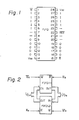
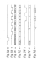
- a write control signal W is fixed to a first pin
- input date IN (l 0 to l 8 ) is fixed to second to sixth pins and 24-th to 27-th pins
- a read control signal R is fixed to a 15-th pin
- output data OUT (O o to Os) is fixed to 9-th to 13-th pins and 16-th to 19-th pins.
- V cc and V ss designate power supplies, and other terminals are designated "Full", "Empty” and the like.
- FIFO (1) is used for data transmission from A-side to B-side
- FIFO (2) is used for data transmission from B-side to A-side.
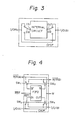
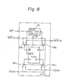
- a one-directional internal circuit has an internal input port IN and an internal output port OUT.
- the internal input port IN is connectable to either an A-side external input/output terminal I/0 (A) or a B-side external input/output terminal I/0 (B).
- the switching of such connections is carried out by a switching means, so that the internal ports I/O (A) and I/O (B), and the internal output port OUT is connected to the other external port.
- a frame indicated by a dotted-solid line designates one chip.
- a frame indicated by a dotted-solid line designates one chip.
- only one FIFO memory is provided as the one-directional internal circuit.
- internal ports such as a write control port W , a read control port R , an input port IN, an output port OUT, and a reset port RST i are provided.
- A-side external ports such as a write/read control port W/R (A) and an input/output port I/O (A)
- B-side external ports such as a write/read control port W/R (B), an input/output I/0 (B), and a reset port RST for the connections to the exterior.
- the external reset port RST is fixed to the internal reset port
- a first switch SW 1 is provided between the external ports W/R (A), W/R (B) and the internal port W ;
- a second switch SW 2 is provided between the external ports W/R (A), W/R (B) and the internal port R ;
- a third switch SW 3 is provided between the external ports I/0 (A), I/0 (B) and the internal port IN;
- a fourth switch SW 4 is provided between the external ports I/0 (A), I/O (B) and the internal port OUT.
- the internal ports IN and OUT, and the external ports I/0 (A) and I/O (B) of Fig. 4 actually have a multi-bit configuration such as a 9-bit configuration as illustrated in Fig. 1, but, for simplification, such ports have a single-bit configuration in Fig. 4.
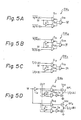
- the switch SW 1 is comprised of NAND circuits G 11 , G 12 , and G 13 , and an inverter I 1 . Therefore, when the mode signal m is "1", the signal at the external control port W/R (A) is supplied to the write control port W of the FIFO memory, and when the mode signal M is "0", the signal at the external control port W/R (B) is supplied to the write control port W of the FIFO memory.
- the switch SW 2 is comprised of NAND circuits G 21 , G 22 , and G 23 , and an inverter 1 2 . Therefore, when the mode signal M is "1", the signal at the external control port W/R (B) is supplied to the write control port W of the FIFO memory, and when the mode signal M is "0", the signal at the external control port W/R (A) is supplied to the write control port W of the FIFO memory.
- the switch SW 3 is comprised of the NAND circuits G 31 , G 32 , and G 33 , and an inverter 1 3 . Therefore, when the mode signal M is "1", the signal at the external port I/O (A) is supplied to the input data port IN of the FIFO memory, and when the mode signal M is "0", the signal at the external port I/0 (B) is supplied to input data port IN of the FIFO memory.
- the switch SW 4 is comprised of NAND circuits Ga 41 , G 42 , G 43 , and G 44 , inverter l 4 to l 8 and CMOS buffers BF 1 and BF 2 . Therefore, when the mode signal M is "1", the lower-side circuit of Fig. 5D is operated so that data at the output data port OUT is transmitted to the B-side port I/0 (B), and when the mode signal M is "0", the upper-side circuit of Fig. 5D is operated so that data at the output data port OUT is transmitted to the A-side port I/O (A).
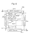
- a static memory cell MC ij is provided between a write word line WL i (W), and a read word line WL; (R), and in write bit lines BL j (W),
- write data IN is written by a write amplifier WA into the memory cell MC ij between a word line such as WL i (W) selected by a write pointer WP (1) and write bit lines such as BL j (W), BL j (W) selected by a write pointer WP (2).
- data of a memory cell between a read word line such as WL; (R) selected by a read pointer RP (1) and read bit lines such as BL i (R), BL j (R) selected by a read pointer RP (2) is read and is transmitted as output data OUT via a read amplifier RA.
- the write pointer WP (1) and WP (2) are counted up one by one in accordance with a write control signal W , thereby sequentially accessing the memory cells and writing data thereinto.
- the two write pointers serve as one write pointer WP and are reset by a reset signal RST. That is, every time one of the write pointers WP (1) and WP (2) is cycled, the other pointer is counted up by + 1.
- the read pointer RP (1) and RP (2) are counted up one by one in accordance with a read control signal R , thereby sequentially accessing the memory cells and reading data therefrom.
- the two read pointers serve as one read pointer RP and are reset by a reset signal RST. That is, every time one of the read pointers RP (1) and RP (2) is cycled, the other pointer is counted up by + 1.
- a mode setting circuit SC for generating the mode signal M is added to the elements of the first embodiment of Fig. 4.
- the mode setting circuit SC detects the presence or absence of an overlap at a predetermined level such as "0" level of the signals of at least two originally existing external ports such as RST and W/R (B) without additional special ports, thereby generating the mode signal M within the chip.
- the mode setting circuit SC of Fig. 8 will be explained with reference to Fig. 9.
- the mode setting circuit SC is comprised of an overlap detector (NOR circuit) DET1 for detecting an overlap of a low level ("0") of the external reset signal RST and a low level of an external write/read control signal R/W (B), a fall detector DET2 comprised of a delay circuit DL, an inverter I 1 , and a NOR circuit Gz , and an RS flip-flop FF serving as a memory.
- This RS flip-flop FF is constructed as shown in Fig. 10.
- a power supply V cc is applied to a set terminal S
- a ground potential is applied to reset terminal R
- the output of the overlap detector DET1 is applied to a clock terminal CK
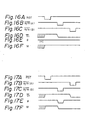
- the output of the fall detector DET2 is applied to a clear terminal CL. Therefore, as illustrated in Figs. 11 A through 11 E, after the FIFO memory is reset by the signal RST
- the flip-flop FF is reset (cleared) by the reset signal RST, but such a reset operation can be carried out by applying the power supply if the circuit constants of the flip-flop FF are suitably set.
- the detector DET1 may detect an overlap of a high level between the two external ports, and a rise detector may be used instead of the fall detector DET2.
- the mode signal M is set by an overlap of the signals of the two external input signals RST, W/R (B), but other external input signals can be used.
- a mode setting circuit SC' for generating the mode signal M is added to the elements of the first embodiment of Fig. 4.
- the mode setting circuit SC' detects the sequence of the signals of at least two originally existing external ports such as W/R (A) and W/R (B) without additional special ports, thereby generating the mode signal M within the chip.
- the mode setting circuit SC' of Fig. 13 will be explained with reference to Fig. 14.
- the mode setting circuit SC' is comprised of two RS flip-flops FF1 and FF2 each of which is constructed as shown in Fig. 15.
- a power supply V cc is applied to a set terminal S
- a ground potential is applied to a reset terminal R
- the reset signal RST is applied to a clear terminal CL
- the signal at the A-side external input/output control port W/R (A) is applied to a clock terminal CK.
- a power supply V cc is applied to a set terminal_S, a ground potential is applied to a reset terminal R, a reset signal RST is applied to clear terminal CL, and the signal ⁇ is applied to a clock terminal CK.
- the output Q of the flip-flop FF2 serves as the mode signal M.
- the flip-flops FF1 and FF2 are reset (cleared) by the reset signal RST, but such a reset operation can be carried out by applying power supply if the circuit constants of the flip-flops FF1 and FF2 are suitably set.
- the mode signal M is determined by which of the A-side input/output control port W/R (A) and the B-side input/output control port W/R (B) receives a preceding pulse.
- an FIFO memory is used as a one-directional circuit, however, the present invention can be applied to other circuits such as LIFO and a shift register.
- the bidirectional semiconductor device is constructed by only one one-directional circuit, the board occupied area on a printed circuit board can be reduced, and in addition, the connections thereof can be simplified.
Landscapes
- Engineering & Computer Science (AREA)
- Theoretical Computer Science (AREA)
- Physics & Mathematics (AREA)
- General Engineering & Computer Science (AREA)
- General Physics & Mathematics (AREA)
- Microelectronics & Electronic Packaging (AREA)
- Computer Hardware Design (AREA)
- Dram (AREA)
- Static Random-Access Memory (AREA)
Applications Claiming Priority (6)
| Application Number | Priority Date | Filing Date | Title |
|---|---|---|---|
| JP61298895A JPS63152084A (ja) | 1986-12-17 | 1986-12-17 | 双方向性半導体装置 |
| JP61298887A JPS63152083A (ja) | 1986-12-17 | 1986-12-17 | 双方向性半導体装置 |
| JP298895/86 | 1986-12-17 | ||
| JP298887/86 | 1986-12-17 | ||
| JP300112/86 | 1986-12-18 | ||
| JP61300112A JPS63153787A (ja) | 1986-12-18 | 1986-12-18 | 双方向性半導体装置 |
Publications (3)
| Publication Number | Publication Date |
|---|---|
| EP0272847A2 true EP0272847A2 (de) | 1988-06-29 |
| EP0272847A3 EP0272847A3 (en) | 1990-03-28 |
| EP0272847B1 EP0272847B1 (de) | 1994-06-22 |
Family
ID=27338257
Family Applications (1)
| Application Number | Title | Priority Date | Filing Date |
|---|---|---|---|
| EP87310861A Expired - Lifetime EP0272847B1 (de) | 1986-12-17 | 1987-12-10 | Zweirichtungs-Halbleitergerät mit nur einem einzigen Einrichtungsgerät |
Country Status (4)
| Country | Link |
|---|---|
| US (1) | US4825098A (de) |
| EP (1) | EP0272847B1 (de) |
| KR (1) | KR910000153B1 (de) |
| DE (1) | DE3750124D1 (de) |
Families Citing this family (11)
| Publication number | Priority date | Publication date | Assignee | Title |
|---|---|---|---|---|
| US4894558A (en) * | 1988-10-11 | 1990-01-16 | Nec Electronics Inc. | Power saving input buffer for use with a gate array |
| US4906870A (en) * | 1988-10-31 | 1990-03-06 | Atmel Corporation | Low power logic array device |
| US5235543A (en) * | 1989-12-29 | 1993-08-10 | Intel Corporation | Dual port static memory with one cycle read-modify-write |
| US5384730A (en) * | 1991-05-31 | 1995-01-24 | Thunderbird Technologies, Inc. | Coincident activation of pass transistors in a random access memory |
| JPH05151778A (ja) * | 1991-06-05 | 1993-06-18 | Mitsubishi Electric Corp | スタテイツクランダムアクセスメモリおよびその制御方法 |
| US5216295A (en) * | 1991-08-30 | 1993-06-01 | General Instrument Corp. | Current mode logic circuits employing IGFETS |
| US5381528A (en) * | 1992-10-15 | 1995-01-10 | Maxtor Corporation | Demand allocation of read/write buffer partitions favoring sequential read cache |
| KR0140179B1 (ko) * | 1994-12-19 | 1998-07-15 | 김광호 | 불휘발성 반도체 메모리 |
| JPH1073643A (ja) * | 1996-09-02 | 1998-03-17 | Mitsubishi Electric Corp | 半導体装置試験治具 |
| US6029253A (en) * | 1997-10-30 | 2000-02-22 | Micron Electronics, Inc. | Method for synchronizing data with a bi-directional buffer |
| US6055597A (en) * | 1997-10-30 | 2000-04-25 | Micron Electronics, Inc. | Bi-directional synchronizing buffer system |
Family Cites Families (7)
| Publication number | Priority date | Publication date | Assignee | Title |
|---|---|---|---|---|
| JPS5247636A (en) * | 1975-10-15 | 1977-04-15 | Toshiba Corp | Control method for transmitting information |
| US4344132A (en) * | 1979-12-14 | 1982-08-10 | International Business Machines Corporation | Serial storage interface apparatus for coupling a serial storage mechanism to a data processor input/output bus |
| US4481623A (en) * | 1982-11-23 | 1984-11-06 | Burroughs Corporation | Speed independent arbiter switch employing M-out-of-N codes |
| US4621201A (en) * | 1984-03-30 | 1986-11-04 | Trilogy Systems Corporation | Integrated circuit redundancy and method for achieving high-yield production |
| JPS6188538A (ja) * | 1984-10-05 | 1986-05-06 | Fujitsu Ltd | 半導体装置 |
| JPS61263313A (ja) * | 1985-05-17 | 1986-11-21 | Matsushita Electric Ind Co Ltd | セレクタ付ラツチ回路 |
| US4774422A (en) * | 1987-05-01 | 1988-09-27 | Digital Equipment Corporation | High speed low pin count bus interface |
-
1987
- 1987-12-08 US US07/130,630 patent/US4825098A/en not_active Expired - Lifetime
- 1987-12-10 EP EP87310861A patent/EP0272847B1/de not_active Expired - Lifetime
- 1987-12-10 DE DE3750124T patent/DE3750124D1/de not_active Expired - Lifetime
- 1987-12-17 KR KR8714385A patent/KR910000153B1/ko not_active Expired
Also Published As
| Publication number | Publication date |
|---|---|
| DE3750124D1 (de) | 1994-07-28 |
| EP0272847B1 (de) | 1994-06-22 |
| US4825098A (en) | 1989-04-25 |
| KR880008338A (ko) | 1988-08-30 |
| EP0272847A3 (en) | 1990-03-28 |
| KR910000153B1 (en) | 1991-01-21 |
Similar Documents
| Publication | Publication Date | Title |
|---|---|---|
| US4159541A (en) | Minimum pin memory device | |
| US5818350A (en) | High performance method of and system for selecting one of a plurality of IC chip while requiring minimal select lines | |
| US4535427A (en) | Control of serial memory | |
| US4825098A (en) | Bidirectional semiconductor device having only one one-directional device | |
| KR900000048B1 (ko) | Lsi 메모리회로 | |
| EP1402340B1 (de) | Fifo-speicher system und verfahren dafür | |
| EP0444825A2 (de) | Registerschaltung für Abfragedurchlauf | |
| JPH1011971A (ja) | 半導体記憶装置 | |
| US5239509A (en) | Semiconductor memory device | |
| EP0416513A2 (de) | FIFO-Speicher | |
| EP0204130B1 (de) | Gerät zur Verminderung des Bedarfs an Prüfdatenspeicher zur Prüfung von Hochgeschwindigkeits-VLSI-Schaltungen | |
| US4922457A (en) | Serial access memory system provided with improved cascade buffer circuit | |
| US6998873B2 (en) | Data input/output buffer and semiconductor memory device using the same | |
| US6366979B1 (en) | Apparatus and method for shorting retransmit recovery times utilizing cache memory in high speed FIFO | |
| US4935902A (en) | Sequential access memory | |
| JPS63153787A (ja) | 双方向性半導体装置 | |
| KR0158249B1 (ko) | 직렬억세스 메모리 장치 | |
| SU1026163A1 (ru) | Устройство дл управлени записью и считыванием информации | |
| JPH027284A (ja) | 集積回路 | |
| KR950009237B1 (ko) | 동기식 반도체 메모리 장치의 데이타 처리방법 | |
| SU1642525A1 (ru) | Многофункциональный запоминающий модуль дл логической матрицы | |
| SU743035A1 (ru) | Запоминающее устройство | |
| JP2595707B2 (ja) | メモリ装置 | |
| SU1531172A1 (ru) | Параллельный асинхронный регистр | |
| KR100680457B1 (ko) | 난드 플래시 메모리 소자의 데이터 출력 회로 및 이를이용한 데이터 출력 방법 |
Legal Events
| Date | Code | Title | Description |
|---|---|---|---|
| PUAI | Public reference made under article 153(3) epc to a published international application that has entered the european phase |
Free format text: ORIGINAL CODE: 0009012 |
|
| AK | Designated contracting states |
Kind code of ref document: A2 Designated state(s): DE FR GB |
|
| PUAL | Search report despatched |
Free format text: ORIGINAL CODE: 0009013 |
|
| AK | Designated contracting states |
Kind code of ref document: A3 Designated state(s): DE FR GB |
|
| 17P | Request for examination filed |
Effective date: 19900921 |
|
| 17Q | First examination report despatched |
Effective date: 19921125 |
|
| GRAA | (expected) grant |
Free format text: ORIGINAL CODE: 0009210 |
|
| AK | Designated contracting states |
Kind code of ref document: B1 Designated state(s): DE FR GB |
|
| REF | Corresponds to: |
Ref document number: 3750124 Country of ref document: DE Date of ref document: 19940728 |
|
| PG25 | Lapsed in a contracting state [announced via postgrant information from national office to epo] |
Ref country code: DE Effective date: 19940923 |
|
| ET | Fr: translation filed | ||
| PGFP | Annual fee paid to national office [announced via postgrant information from national office to epo] |
Ref country code: GB Payment date: 19941130 Year of fee payment: 8 |
|
| PLBE | No opposition filed within time limit |
Free format text: ORIGINAL CODE: 0009261 |
|
| STAA | Information on the status of an ep patent application or granted ep patent |
Free format text: STATUS: NO OPPOSITION FILED WITHIN TIME LIMIT |
|
| 26N | No opposition filed | ||
| PG25 | Lapsed in a contracting state [announced via postgrant information from national office to epo] |
Ref country code: GB Effective date: 19951210 |
|
| GBPC | Gb: european patent ceased through non-payment of renewal fee |
Effective date: 19951210 |
|
| PGFP | Annual fee paid to national office [announced via postgrant information from national office to epo] |
Ref country code: FR Payment date: 20031210 Year of fee payment: 17 |
|
| PG25 | Lapsed in a contracting state [announced via postgrant information from national office to epo] |
Ref country code: FR Free format text: LAPSE BECAUSE OF NON-PAYMENT OF DUE FEES Effective date: 20050831 |
|
| REG | Reference to a national code |
Ref country code: FR Ref legal event code: ST |