EP0348933B1 - Standardzelle - Google Patents
Standardzelle Download PDFInfo
- Publication number
- EP0348933B1 EP0348933B1 EP89111757A EP89111757A EP0348933B1 EP 0348933 B1 EP0348933 B1 EP 0348933B1 EP 89111757 A EP89111757 A EP 89111757A EP 89111757 A EP89111757 A EP 89111757A EP 0348933 B1 EP0348933 B1 EP 0348933B1
- Authority
- EP
- European Patent Office
- Prior art keywords
- cell
- power source
- cells
- source wires
- standard
- Prior art date
- Legal status (The legal status is an assumption and is not a legal conclusion. Google has not performed a legal analysis and makes no representation as to the accuracy of the status listed.)
- Expired - Lifetime
Links
- XAGFODPZIPBFFR-UHFFFAOYSA-N aluminium Chemical compound [Al] XAGFODPZIPBFFR-UHFFFAOYSA-N 0.000 description 1
- 229910052782 aluminium Inorganic materials 0.000 description 1
- 239000004411 aluminium Substances 0.000 description 1
- 230000001934 delay Effects 0.000 description 1
- 238000000034 method Methods 0.000 description 1
- 230000004048 modification Effects 0.000 description 1
- 238000012986 modification Methods 0.000 description 1
Images


Classifications
-
- H—ELECTRICITY
- H10—SEMICONDUCTOR DEVICES; ELECTRIC SOLID-STATE DEVICES NOT OTHERWISE PROVIDED FOR
- H10D—INORGANIC ELECTRIC SEMICONDUCTOR DEVICES
- H10D89/00—Aspects of integrated devices not covered by groups H10D84/00 - H10D88/00
- H10D89/10—Integrated device layouts
-
- G—PHYSICS
- G11—INFORMATION STORAGE
- G11C—STATIC STORES
- G11C11/00—Digital stores characterised by the use of particular electric or magnetic storage elements; Storage elements therefor
- G11C11/21—Digital stores characterised by the use of particular electric or magnetic storage elements; Storage elements therefor using electric elements
- G11C11/34—Digital stores characterised by the use of particular electric or magnetic storage elements; Storage elements therefor using electric elements using semiconductor devices
- G11C11/40—Digital stores characterised by the use of particular electric or magnetic storage elements; Storage elements therefor using electric elements using semiconductor devices using transistors
- G11C11/41—Digital stores characterised by the use of particular electric or magnetic storage elements; Storage elements therefor using electric elements using semiconductor devices using transistors forming static cells with positive feedback, i.e. cells not needing refreshing or charge regeneration, e.g. bistable multivibrator or Schmitt trigger
-
- G—PHYSICS
- G11—INFORMATION STORAGE
- G11C—STATIC STORES
- G11C5/00—Details of stores covered by group G11C11/00
-
- G—PHYSICS
- G11—INFORMATION STORAGE
- G11C—STATIC STORES
- G11C5/00—Details of stores covered by group G11C11/00
- G11C5/06—Arrangements for interconnecting storage elements electrically, e.g. by wiring
- G11C5/063—Voltage and signal distribution in integrated semi-conductor memory access lines, e.g. word-line, bit-line, cross-over resistance, propagation delay
-
- G—PHYSICS
- G11—INFORMATION STORAGE
- G11C—STATIC STORES
- G11C8/00—Arrangements for selecting an address in a digital store
- G11C8/14—Word line organisation; Word line lay-out
Definitions
- the present invention relates to a standard cell laid out for LSI (large scale integrated circuit), and particularly to a large scale standard cell like a flip-flop standard cell (a so called bistable standard cell) whose length in the direction of the power source wire thereof can be controlled so as not to be larger than required.
- LSI large scale integrated circuit
- a conventional standard cell used for a layout of a large scale integrated circuit, particularly a large scale cell like a flip-flop standard cell has a relatively large length in the direction of the power source wire thereof (hereinafter the direction is called lateral direction) as compared with cells other than the flip-flop cell.
- the direction is called lateral direction
- dead space tends to be produced in the circuit pattern owing to the uniformity of their lateral lengths. Accordingly, there is inconvenience in design of the circuit patterns as composed by the combination.
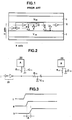
- Fig. 1 shows a composition of a conventional standard cell.
- the cell there is provided in the cell two power source wires 1, 1 extending substantially in parallel to the lateral direction (X axis) of the cell so that a group of circuit elements such as transistors and diodes for composing a logical circuit required are arranged in a space 2 defined between the two power source wires 1, 1.
- Fig. 2 shows a manner of a cell from which the clock skew tends to occur
- Fig. 3 shows waveforms produced by the clock skew shifting in timing from an original clock.
- a clock signal (a) inputted to a cell A and a clock signal (b) inputted to a cell B are different from each other in their time constants of a wire resistance Ri and a wire capacity Ci between the buffer 21 and the cell A, and a wire resistance R and capacity C between the buffer 21 and the cell B.
- the clock line of this clock skew becomes long and large, in the case that flip-flop cells are scattered. Accordingly, if all the flip-flop cells are arranged in one cell row, it is useful in order to make the clock skew small. However, if the flip-flop cells are conventional ones, the following problems occur.
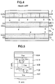
- Fig. 4 shows an abstract layout of a portion of IC composed by conventional cells, in which are shown a cell row including only flip-flop cells 3 and other cell rows including cells 4 other than the flip-flop cell. As seen from the drawing, there are dead spaces 5 produced by the differences of lateral length of the rows of the flip-flop cells and the others. Accordingly, an area of the circuit pattern composed with the conventional cells by automatic place and route should become larger than required.
- the conventional standard cell has only two power source wires 1, 1, thus it is impossible to connect cells inversely between the wires of the high potential side (V DD ) and the low potential side (v SS ) in one cell row.
- a flip-flop (bistable) standard cell whose lateral length can be controlled so as not to be larger than required, whereby an area of the cell and an entire area of a circuit pattern composed with the cells by automatic place and route can be reduced.
- a standard cell according to the present invention for automatic place and route is provided with at least three power source wires as set out in claim 1.
- the circuit elements such as transistors and diodes for composing a logical circuit can be arranged in at least two spaces respectively defined between each adjacent pair of the wires. Accordingly, when compared the lateral lengths of the standard cells according to the present invention and the prior art required for arranging the same number of the elements therein, the length of the former can be reduced to substantially half or less as compared with that of the latter because the elements can be arranged in at least two spaces in the case of the former.
- the electrical potentials of respective wires can be arranged symmetrically in the vertical direction of the cell, thus it becomes possible to optionally change the vertical direction of the cell in one cell row.
- Fig. 5 shows a basic composition of a standard cell according to the present invention.
- the standard cell for automatic place and route according to the present invention is provided with at least three power source wires 10.
- the central one of the power source wires 10 is a low potential power source wire and the outside two power source wires are high potential power source wires. Accordingly, there can be obtained at least two spaces 11, 11 defined between each adjacent pair of the wires for arrangement of circuit elements such as transistors and diodes for composing a logical circuit.
- the length of the former can be substantially reduced to half or less to that of the latter because the elements can be arranged in at least two spaces in the case of the former.
- the vertical length of the cell increases as the number of the power source wires increases. However, when the number of the power source wires becomes three, the vertical length of the cell is increased by only 1.5 times that of the prior art cell having two power source wires.
- the electrical potentials of respective wires can be arranged symmetrically in the vertical direction of the cell, thus it becomes possible to optionally change the vertical direction of the cell in one cell row.
- Fig. 6 shows an abstract layout of a portion of IC of an embodiment of the present invention.
- a plurality of flip-flop cells 7 are assembled together in one row 12, and other cells are assembled in the other rows 13, 13.
- Reference numerals 14 designate wiring areas respectively.
- each the lateral length of the cells 7 can be optionally reduced into a desired length.
- the length of the row 12 comprising the flip-flop cells of an embodiment according to the present invention shown in Fig. 6 can be adjusted to substantially the same as that of the rows 13, 13, so there can be eliminated the dead space 5 as produced in the composition of the standard cell comprising a combination of a conventional flip-flop cell and other cells as shown in Fig. 4.
- Figs. 7 and 8 show an embodiment of a connecting cell 13 according to the present invention for connecting two kinds of cells having a different number of power source wires from each other, more specifically, the drawings show the case on which are connected cells having three power source wires and other cells having two power source wires, the wires consisting of aluminium. Further in the drawings, there are shown vias H and a connecting strip 16.
- a plurality of the connecting cells 13 should be required and the entire lateral length of the connected cells increases by the length corresponding to the number of the connecting cells employed.
- wiring in the area becomes extremely difficult. While, as shown in Fig. 10, when the cells having the same number of wires are respectively assembled together, these two kinds of assembled cells can be connected with only one connecting cell 13.
- each wire 19 for connecting each pair of then input terminals 17 and the output terminals 18 of each adjacent pair of the cells should be relatively long.
- the electrical potentials of respective power source wires can be optionally arranged to be vertically symmetrical.
- the directions of the cells can be so arranged that each the pair of the input terminal 17 and the output terminal 18 to be connected can be adjacent to each other to shorten the wire 19. This method is applicable to other cases on which different kinds of cells are connected.
- the area for arranging circuit elements therein can be increased in the vertical direction by increase of the number of the power source wires in a standard cell according to the present invention, thus the elements can be flexibly arranged in the cell, so that the lateral length of the cell can be reduced as compared with conventional cells on condition that the same number of the elements are respectively arranged.
- the electrical potentials of respective power source wires can be arranged vertically symmetrical in the cell according to the present invention, the direction of the cell can be changed vertically in one cell row. Accordingly, there can be shortened wires for connecting cells respectively having an input and an output terminal which are vertically disposed away from each other. Moreover, an entire area of a circuit pattern formed by automatic place and route can be also reduced.
Landscapes
- Engineering & Computer Science (AREA)
- Microelectronics & Electronic Packaging (AREA)
- Computer Hardware Design (AREA)
- Design And Manufacture Of Integrated Circuits (AREA)
- Semiconductor Integrated Circuits (AREA)
Claims (5)
- Standardzelle zur automatischen Plazierung und Leitungsführung von Schaltkreiselementen eines hochintegrierten Schaltkreises (LSI), dadurch gekennzeichnet, daß sie mindestens drei Energiequellenleitungen (10A, 10B, 10C) umfaßt, die sich im wesentlichen nur in einer Richtung (x-Achse) der Zelle erstrecken, wobei jedes benachbarte Paar (10A, 10B; 10B, 10C) der Energiequellenleitungen in paralleler und voneinander beabstandeter Beziehung angeordnet ist, um einen Zwischenraum (11A; 11B) zu bilden, in welchem die Schaltkreiselemente der Standardzelle angeordnet sind.
- Standardzelle nach Anspruch 1, dadurch gekennzeichnet, daß eine der Energiequellenleitungen (10B) eine Energiequellenleitung niedrigen Potentials (VSS) und die andere Energiequellenleitung (10A, 10C) eine Energiequellenleitung hohen Potentials (VDD) ist.
- Standardzelle nach Anspruch 1 dadurch gekennzeichnet, daß die elektrischen Potentiale von mindestens drei Energiequellenleitungen zur mittleren Energiequellenleitung (10B) nach ihren beiden Außenseiten symmetrisch angeordnet sind.
- Anordnung von mindestens zwei Standardzellen, umfassend:
Eine erste Standardzelle (C₁) mit mindestens drei Energiequellenleitungen (10), wie in einem der Ansprüche 1 bis 3 beansprucht;
eine zweite Standardzelle (10₂) mit mindestens zwei Energiequellenleitungen (15);
eine Verbindungszelle (13) zum Verbinden der ersten und zweiten Standardzelle. - Anordnung von Standardzellen nach Anspruch 4, dadurch gekennzeichnet, daß eine Vielzahl von ersten Standardzellen zusammengefaßt ist, um eine erste Standardzellengruppe (C₁ in Fig. 10) zu bilden, eine Vielzahl von zweiten Standardzellen zusammengefaßt ist, um eine zweite Standardzellengruppe (C₂ in Fig. 10) zu bilden und die ersten und zweiten Zellengruppen durch eine einzige Verbindungszelle (13) verbunden sind.
Applications Claiming Priority (2)
| Application Number | Priority Date | Filing Date | Title |
|---|---|---|---|
| JP158005/88 | 1988-06-28 | ||
| JP63158005A JP2739958B2 (ja) | 1988-06-28 | 1988-06-28 | スタンダードセル |
Publications (3)
| Publication Number | Publication Date |
|---|---|
| EP0348933A2 EP0348933A2 (de) | 1990-01-03 |
| EP0348933A3 EP0348933A3 (en) | 1990-11-28 |
| EP0348933B1 true EP0348933B1 (de) | 1994-05-11 |
Family
ID=15662174
Family Applications (1)
| Application Number | Title | Priority Date | Filing Date |
|---|---|---|---|
| EP89111757A Expired - Lifetime EP0348933B1 (de) | 1988-06-28 | 1989-06-28 | Standardzelle |
Country Status (5)
| Country | Link |
|---|---|
| US (1) | US5401988A (de) |
| EP (1) | EP0348933B1 (de) |
| JP (1) | JP2739958B2 (de) |
| KR (1) | KR940001393B1 (de) |
| DE (1) | DE68915211T2 (de) |
Families Citing this family (6)
| Publication number | Priority date | Publication date | Assignee | Title |
|---|---|---|---|---|
| JPH06140505A (ja) * | 1992-10-28 | 1994-05-20 | Mitsubishi Electric Corp | 半導体集積回路装置 |
| US5675501A (en) * | 1994-03-15 | 1997-10-07 | Kabushiki Kaisha Toshiba | Method of designing semiconductor integrated circuit apparatus having no dead space |
| DE69517693T2 (de) * | 1995-12-29 | 2001-03-01 | Stmicroelectronics S.R.L., Agrate Brianza | Standardzellenbibliothek für den Entwurf von integrierten Schaltungen |
| US5949261A (en) | 1996-12-17 | 1999-09-07 | Cypress Semiconductor Corp. | Method and circuit for reducing power and/or current consumption |
| US6255675B1 (en) * | 1998-07-10 | 2001-07-03 | Xilinx, Inc. | Programmable capacitor for an integrated circuit |
| US6963510B1 (en) | 1998-07-10 | 2005-11-08 | Xilinx, Inc. | Programmable capacitor and method of operating same |
Family Cites Families (18)
| Publication number | Priority date | Publication date | Assignee | Title |
|---|---|---|---|---|
| GB1579419A (en) * | 1977-06-15 | 1980-11-19 | Seiko Instr & Electronics | Static induction transistor logic semi-conductor devices and integrated injection logic semi-conductor devices |
| JPS5925381B2 (ja) * | 1977-12-30 | 1984-06-16 | 富士通株式会社 | 半導体集積回路装置 |
| US4198695A (en) * | 1978-07-19 | 1980-04-15 | Texas Instruments Incorporated | Static semiconductor memory cell using data lines for voltage supply |
| US4295149A (en) * | 1978-12-29 | 1981-10-13 | International Business Machines Corporation | Master image chip organization technique or method |
| US4423432A (en) * | 1980-01-28 | 1983-12-27 | Rca Corporation | Apparatus for decoding multiple input lines |
| JPS5827343A (ja) * | 1981-08-10 | 1983-02-18 | Matsushita Electronics Corp | 半導体集積回路 |
| JPS58142544A (ja) * | 1982-02-19 | 1983-08-24 | Hitachi Ltd | 半導体集積回路 |
| JPS58166742A (ja) * | 1982-03-29 | 1983-10-01 | Nec Corp | マスタ−スライス基板 |
| US4516040A (en) * | 1982-06-14 | 1985-05-07 | Standard Microsystems Corporation | High-speed merged plane logic function array |
| JPS607147A (ja) * | 1983-06-24 | 1985-01-14 | Mitsubishi Electric Corp | 半導体装置 |
| JPS60198843A (ja) * | 1984-03-23 | 1985-10-08 | Fujitsu Ltd | マスタ−スライス方式集積回路 |
| JPS6124250A (ja) * | 1984-07-13 | 1986-02-01 | Nippon Gakki Seizo Kk | 半導体集積回路装置 |
| JPS61185964A (ja) * | 1985-02-13 | 1986-08-19 | Toshiba Corp | 半導体メモリ |
| JPS6320440U (de) * | 1986-07-25 | 1988-02-10 | ||
| US4949149A (en) * | 1987-03-31 | 1990-08-14 | Unisys Corporation | Semicustom chip whose logic cells have narrow tops and wide bottoms |
| JP2606845B2 (ja) * | 1987-06-19 | 1997-05-07 | 富士通株式会社 | 半導体集積回路 |
| JPS6437034A (en) * | 1987-08-01 | 1989-02-07 | Ricoh Kk | Standard cell |
| US4851893A (en) * | 1987-11-19 | 1989-07-25 | Exar Corporation | Programmable active/passive cell structure |
-
1988
- 1988-06-28 JP JP63158005A patent/JP2739958B2/ja not_active Expired - Lifetime
-
1989
- 1989-06-28 DE DE68915211T patent/DE68915211T2/de not_active Expired - Fee Related
- 1989-06-28 KR KR1019890008920A patent/KR940001393B1/ko not_active Expired - Fee Related
- 1989-06-28 EP EP89111757A patent/EP0348933B1/de not_active Expired - Lifetime
-
1992
- 1992-11-10 US US08/974,322 patent/US5401988A/en not_active Expired - Lifetime
Non-Patent Citations (1)
| Title |
|---|
| VLSI SYSTEM DESIGNS, S. MUROGA, John Wiley & Sons, New York, US; pages 389-392 * |
Also Published As
| Publication number | Publication date |
|---|---|
| JP2739958B2 (ja) | 1998-04-15 |
| KR900001007A (ko) | 1990-01-31 |
| JPH029149A (ja) | 1990-01-12 |
| KR940001393B1 (ko) | 1994-02-21 |
| US5401988A (en) | 1995-03-28 |
| DE68915211D1 (de) | 1994-06-16 |
| DE68915211T2 (de) | 1994-09-29 |
| EP0348933A2 (de) | 1990-01-03 |
| EP0348933A3 (en) | 1990-11-28 |
Similar Documents
| Publication | Publication Date | Title |
|---|---|---|
| US5045725A (en) | Integrated standard cell including clock lines | |
| KR100273495B1 (ko) | 반도체 기억장치 | |
| US4811073A (en) | Gate array arrangement | |
| US4661721A (en) | Clock driver distribution system in a semiconductor integrated circuit device | |
| US5422441A (en) | Master slice integrated circuit having a reduced chip size and a reduced power supply noise | |
| US4689441A (en) | Routing method and pattern for reducing cross talk noise problems on printed interconnection boards | |
| EP0112894B1 (de) | Stromversorgungsführung für eine torschaltungsanordnung | |
| US4513307A (en) | CMOS/SOS transistor gate array apparatus | |
| EP0304930B1 (de) | Integrierte Halbleiterschaltung mit Signallinien | |
| US5012427A (en) | Semiconductor integrated circuit and method of manufacturing the same | |
| US4644187A (en) | Gate array basic cell | |
| US6329969B1 (en) | Integrated circuit for driving liquid crystal | |
| EP0348933B1 (de) | Standardzelle | |
| EP0335697B1 (de) | Integrierte Schaltung mit einer Verbindungsverdrahtung | |
| KR100261900B1 (ko) | 반도체 집적 회로 장치 | |
| US5391904A (en) | Semiconductor delay circuit device | |
| US6456137B1 (en) | Semiconductor circuit, delay adjustment method therefor and layout method therefor | |
| US5506428A (en) | Gate array LSI | |
| KR100261901B1 (ko) | 클럭 드라이버 회로 및 반도체 집적 회로 장치 | |
| JPS61226943A (ja) | 自動配置配線用標準セル | |
| US5227665A (en) | Semiconductor integrated circuit device | |
| US5475568A (en) | Power supply structure for multichip package | |
| EP0278463A2 (de) | Gatematrix mit in Verbindungsgebiet begrabenem Transistor | |
| GB2122417A (en) | Integrated circuits | |
| JPH0560666B2 (de) |
Legal Events
| Date | Code | Title | Description |
|---|---|---|---|
| PUAI | Public reference made under article 153(3) epc to a published international application that has entered the european phase |
Free format text: ORIGINAL CODE: 0009012 |
|
| 17P | Request for examination filed |
Effective date: 19890628 |
|
| AK | Designated contracting states |
Kind code of ref document: A2 Designated state(s): DE FR GB |
|
| RAP1 | Party data changed (applicant data changed or rights of an application transferred) |
Owner name: TOSHIBA MICRO-ELECTRONICS CORPORATION Owner name: KABUSHIKI KAISHA TOSHIBA |
|
| PUAL | Search report despatched |
Free format text: ORIGINAL CODE: 0009013 |
|
| AK | Designated contracting states |
Kind code of ref document: A3 Designated state(s): DE FR GB |
|
| 17Q | First examination report despatched |
Effective date: 19921208 |
|
| GRAA | (expected) grant |
Free format text: ORIGINAL CODE: 0009210 |
|
| AK | Designated contracting states |
Kind code of ref document: B1 Designated state(s): DE FR GB |
|
| REF | Corresponds to: |
Ref document number: 68915211 Country of ref document: DE Date of ref document: 19940616 |
|
| ET | Fr: translation filed | ||
| PLBE | No opposition filed within time limit |
Free format text: ORIGINAL CODE: 0009261 |
|
| STAA | Information on the status of an ep patent application or granted ep patent |
Free format text: STATUS: NO OPPOSITION FILED WITHIN TIME LIMIT |
|
| 26N | No opposition filed | ||
| PGFP | Annual fee paid to national office [announced via postgrant information from national office to epo] |
Ref country code: FR Payment date: 19970610 Year of fee payment: 9 |
|
| PGFP | Annual fee paid to national office [announced via postgrant information from national office to epo] |
Ref country code: DE Payment date: 19970704 Year of fee payment: 9 |
|
| PG25 | Lapsed in a contracting state [announced via postgrant information from national office to epo] |
Ref country code: FR Free format text: LAPSE BECAUSE OF NON-PAYMENT OF DUE FEES Effective date: 19990226 |
|
| PG25 | Lapsed in a contracting state [announced via postgrant information from national office to epo] |
Ref country code: DE Free format text: LAPSE BECAUSE OF NON-PAYMENT OF DUE FEES Effective date: 19990401 |
|
| REG | Reference to a national code |
Ref country code: FR Ref legal event code: ST |
|
| REG | Reference to a national code |
Ref country code: GB Ref legal event code: IF02 |
|
| PGFP | Annual fee paid to national office [announced via postgrant information from national office to epo] |
Ref country code: GB Payment date: 20070627 Year of fee payment: 19 |
|
| GBPC | Gb: european patent ceased through non-payment of renewal fee |
Effective date: 20080628 |
|
| PG25 | Lapsed in a contracting state [announced via postgrant information from national office to epo] |
Ref country code: GB Free format text: LAPSE BECAUSE OF NON-PAYMENT OF DUE FEES Effective date: 20080628 |