EP0347725B1 - Tableau élctronique et accessoires tels que les instruments d'écriture - Google Patents
Tableau élctronique et accessoires tels que les instruments d'écriture Download PDFInfo
- Publication number
- EP0347725B1 EP0347725B1 EP89110724A EP89110724A EP0347725B1 EP 0347725 B1 EP0347725 B1 EP 0347725B1 EP 89110724 A EP89110724 A EP 89110724A EP 89110724 A EP89110724 A EP 89110724A EP 0347725 B1 EP0347725 B1 EP 0347725B1
- Authority
- EP
- European Patent Office
- Prior art keywords
- writing
- electric wave
- electronic blackboard
- signal
- detection means
- Prior art date
- Legal status (The legal status is an assumption and is not a legal conclusion. Google has not performed a legal analysis and makes no representation as to the accuracy of the status listed.)
- Expired - Lifetime
Links
- 239000003550 marker Substances 0.000 claims description 35
- 238000001514 detection method Methods 0.000 claims description 32
- 239000003990 capacitor Substances 0.000 claims description 18
- 238000006243 chemical reaction Methods 0.000 claims description 2
- 230000010365 information processing Effects 0.000 claims description 2
- 230000001419 dependent effect Effects 0.000 claims 1
- 230000005540 biological transmission Effects 0.000 description 24
- 230000015654 memory Effects 0.000 description 13
- 238000000034 method Methods 0.000 description 9
- 230000008569 process Effects 0.000 description 7
- 239000007769 metal material Substances 0.000 description 6
- 229920003002 synthetic resin Polymers 0.000 description 5
- 239000000057 synthetic resin Substances 0.000 description 5
- 230000008859 change Effects 0.000 description 4
- 230000006870 function Effects 0.000 description 4
- 230000004044 response Effects 0.000 description 4
- 230000009471 action Effects 0.000 description 3
- 230000002441 reversible effect Effects 0.000 description 3
- 230000008054 signal transmission Effects 0.000 description 3
- 230000007704 transition Effects 0.000 description 3
- 238000004364 calculation method Methods 0.000 description 2
- 238000006073 displacement reaction Methods 0.000 description 2
- 230000004907 flux Effects 0.000 description 2
- 239000000463 material Substances 0.000 description 2
- 239000002023 wood Substances 0.000 description 2
- 239000003086 colorant Substances 0.000 description 1
- 238000004891 communication Methods 0.000 description 1
- 230000008878 coupling Effects 0.000 description 1
- 238000010168 coupling process Methods 0.000 description 1
- 238000005859 coupling reaction Methods 0.000 description 1
- 238000010586 diagram Methods 0.000 description 1
- 239000000428 dust Substances 0.000 description 1
- 238000010030 laminating Methods 0.000 description 1
- 239000002184 metal Substances 0.000 description 1
- 230000003287 optical effect Effects 0.000 description 1
- 239000003973 paint Substances 0.000 description 1
- 239000002985 plastic film Substances 0.000 description 1
- 238000012887 quadratic function Methods 0.000 description 1
- 230000008707 rearrangement Effects 0.000 description 1
- 230000000717 retained effect Effects 0.000 description 1
- 239000000758 substrate Substances 0.000 description 1
- 230000001360 synchronised effect Effects 0.000 description 1
- 230000002123 temporal effect Effects 0.000 description 1
Images


Classifications
-
- G—PHYSICS
- G06—COMPUTING; CALCULATING OR COUNTING
- G06F—ELECTRIC DIGITAL DATA PROCESSING
- G06F3/00—Input arrangements for transferring data to be processed into a form capable of being handled by the computer; Output arrangements for transferring data from processing unit to output unit, e.g. interface arrangements
- G06F3/01—Input arrangements or combined input and output arrangements for interaction between user and computer
- G06F3/03—Arrangements for converting the position or the displacement of a member into a coded form
- G06F3/041—Digitisers, e.g. for touch screens or touch pads, characterised by the transducing means
- G06F3/046—Digitisers, e.g. for touch screens or touch pads, characterised by the transducing means by electromagnetic means
-
- B—PERFORMING OPERATIONS; TRANSPORTING
- B43—WRITING OR DRAWING IMPLEMENTS; BUREAU ACCESSORIES
- B43L—ARTICLES FOR WRITING OR DRAWING UPON; WRITING OR DRAWING AIDS; ACCESSORIES FOR WRITING OR DRAWING
- B43L1/00—Repeatedly-usable boards or tablets for writing or drawing
-
- G—PHYSICS
- G06—COMPUTING; CALCULATING OR COUNTING
- G06F—ELECTRIC DIGITAL DATA PROCESSING
- G06F3/00—Input arrangements for transferring data to be processed into a form capable of being handled by the computer; Output arrangements for transferring data from processing unit to output unit, e.g. interface arrangements
- G06F3/01—Input arrangements or combined input and output arrangements for interaction between user and computer
- G06F3/03—Arrangements for converting the position or the displacement of a member into a coded form
- G06F3/033—Pointing devices displaced or positioned by the user, e.g. mice, trackballs, pens or joysticks; Accessories therefor
- G06F3/0354—Pointing devices displaced or positioned by the user, e.g. mice, trackballs, pens or joysticks; Accessories therefor with detection of 2D relative movements between the device, or an operating part thereof, and a plane or surface, e.g. 2D mice, trackballs, pens or pucks
- G06F3/03545—Pens or stylus
Definitions
- the present invention relates to an electronic blackboard for processing image information which corresponds to the image or the like displayed on the writing surface and its accessaries such as writing tools.
- an electromagnetic coupled type hereinafter
- a multiplicity of sensing lines are, in both x and y directions, formed on the reverse side of the writing surface thereof and a writing tool comprising a felt pen or the like is provided with a coil as to generate flux change when an electronic current is passed so that the thus-generated flux change is detected by the sensing lines or the other end of the coil so that the position of the writing tool on the writing surface is detected and thereby image information which corresponds to the image displayed on the writing surface can be processed.
- a photoelectric transfer type Another type of the electronic blackboard apparatus which is arranged such that image written on a whiteboard or a flexible sheet with a writing tool such as a felt pen or the like is scanned by a scanner which can move along the surface of this whiteboard or by a stationary scanner with this sheet wound up as to be photoelectrically transferred to image information.
- the other conventional electronic blackboard apparatus (called “a pressure sensing type” hereinafter) in which two resistance plates provided with electrodes on the opposing sides thereof are fastened to the reverse side of a writing surface made of a flexible material with laminated to each other. These two resistance plates are fastened to the same in such a manner that these electrodes are positioned in the vertical or lateral direction. Therefore, a displacement current is generated between this electrode and the electrode on the other resistance plate when the writing tool is moved along the surface of the writing surface with an electric current being passed through either of the two resistance plates. On the basis of the thus-generated displacement current, the position of the writing tool on the writing surface is detected so that image information corresponding to the image displayed on the writing surface is processed.
- the above-described electromagnetic coupling type apparatus arises a problem in that, a cord needs to be provided between the control unit for detecting the position and the coil provided for the writing tool. The thus-provided cord deteriorates readiness in handling the writing tool.
- the writing tool can be arranged to be a cord-less type.
- information corresponding to the displayed image cannot be obtained during writing of the image on the writing surface, that is real-time image cannot be obtained since image information can be first obtained when the scanner is moved or the sheet is wound up.
- the writing tool can be arranged to be a cord-less type and the information corresponding to the image which is being written can be obtained.
- a problem arises in that the thickness and the weight become excessive since the structure needs to be formed so as to withstand the pressure applied with the writing tool to the writing surface.
- the document EP-A-0 259 894 discloses a position detecting apparatus which comprises: pen-shaped position designating means (pointer) having a tuning circuit which includes a coil and a capacitor and has a predetermined tuning frequency, a sensing portion provided on a tablet and including electric wave generating means capable of generating electric waves for exciting said tuning circuit, and electric wave detection means capable of detecting electric waves generated by the excited tuning circuit, and coordinate detection means for determining coordinate values of the position of said position designating means relative to the sensing portion, based on the frequency of the electric waves detected by the electric wave detection means.
- pen-shaped position designating means pointer having a tuning circuit which includes a coil and a capacitor and has a predetermined tuning frequency
- a sensing portion provided on a tablet and including electric wave generating means capable of generating electric waves for exciting said tuning circuit
- electric wave detection means capable of detecting electric waves generated by the excited tuning circuit
- coordinate detection means for determining coordinate values of the position of said position designating means relative to the sensing portion, based
- this known position detecting apparatus does not permit the repeated writing and erasing of physically readable characters or graphic items by means of a writing tool and an eraser, as is required for an electronic blackboard. Further, this known apparatus is not capable of determining whether the detected coordinate values have been input by means of a writing tool or by means of an eraser.
- Fig. 1 is a view which illustrates a first embodiment of an electronic blackboard apparatus according to the present invention, wherein reference numeral 1 represents a main blackboard body, 2 represents an instruction rod, 3 represents a marker, 4 represents an eraser, and 5 represents a control box.
- the main blackboard body 1 is formed such that legs 13 are fastened to a frame 12 a portion of which corresponds to the front surface of a sensing portion 11 is made of a non-metallic material having a flat surface so as to form a writing surface 14 which can be repeatedly used with the marker 3 and the eraser 4.
- the portion of the frame 12 which corresponds to the front surface of the sensing portion 11 may be formed by applying paint to which magnetic dust is mixed to the plate made of the non-metallic material or by laminating a film sheet such as a magnet sheet and a plastic sheet on the same plate for the purpose of realizing a writing surface to which sheet in which intended frames or figures are written can be temporally fastened by metal pieces or magnets.
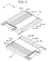
- Fig. 2 is a view which in detail illustrates a loop coil groups 11x in x-direction and a loop coil group 11y in y-direction which form the sensing portion 11.
- the loop coil group 11x in x-direction comprises a multiplicity of, for example, 48 loop coils 11x-1, 11x-2,..., 11x-48 so as to be arranged in parallel to each other and to overlap each other.
- the loop coil group 11y in y-direction comprises a multiplicity of, for example, 30 loop coils 11y-1, 11y-2,..., 11y-30 so as to be arranged in parallel to each other and to overlap each other.
- the loop coils may be formed by a plurality of turns if necessary.
- Fig. 3 is a view which illustrates a first embodiment of the writing tool and so on according to the present invention, in which the structure of the instruction rod 2 is illustrated.
- This instruction rod 2 is made of a synthetic resin, wood or the like and is formed in such a manner that a tuning circuit 22 comprising a coil 221 which includes a core and a capacitor 222 is accommodated in a recessed portion 21a formed at the front end portion of a column-like main body 21 made of a synthetic resin or wood in such a manner that the axis of this coil 221 substantially meets the longitudinal direction of the main body 21 (frame), and this recessed portion 21a is covered with a cap 23 made of the similar material to that for the main body 21.
- the main body 21 may comprise a telescopic rod.
- the coil 221 and the capacitor 222 are, as shown in Fig. 7, connected to each other in series so as to form a known resonant circuit.
- the inductance of this coil 221 and the capacity of the capacitor 222 are determined as to make the resonant (tuned) frequency thereof substantially a predetermined frequency f0, for example, 600 kHz.
- Fig. 4 is a view which illustrates a second embodiment of the writing tool according to the present invention, in which the structure of a marker 3 is in detail illustrated.
- This marker 3 comprises: a pen shaft 31 formed by two portions 31a and 31b made of a non-metallic material such as a synthetic resin and to be screw-coupled with each other; a pen body 32 such as a black felt pen on the market or the like; a push switch 331; a coil 332 including a core; a tuning circuit 33 comprising capacitors 333 and 334; and a cap 34 for the pen body 32.
- the pen body 32 is accommodated in a space formed by a stopper 31a′ formed in the portion 31a of the pen shaft 31 and the switch 331 accommodated in the portion 31b such that the same can be slightly moved therein.
- the coil 332 is accommodated in the portion at the front end of the portion 31a of the pen shaft 31 such that the axial direction thereof can be substantially meet the longitudinal direction of the pen shaft 31 (frame).
- the coil 332 and the capacitor 333 are connected to each other in series so as to form a known resonant circuit.
- the inductance of this coil 332 and the capacity of the capacitor 333 are so determined as to make the resonant (tuned) frequency thereof substantially a predetermined frequency f0, for example, 600 kHz.
- the capacitor 334 is in parallel connected to the two ends of the capacitor 333 via the switch 331 so that the same acts to change the tuned frequency in the resonant circuit from the predetermined frequency f0 to another frequency f1, for example, 550 kHz when the above-described switch 331 is switched on.
- This switch 331 is arranged to be switched on when it is abutted by the rear end of the pen body 32 which has been pushed into the pen shaft 31 as a result of abutting the front end of the pen body 32 against the writing surface 14 or the like with the pen shaft 31 held by the hand or the like.
- the front end of th pen body is made project over the writing surface as to enable the writing according to this embodiment, it may be arranged to be capable of projecting only when used.
- the marker is so designed that the pen body 32 included therein can be replaced by so arranging the pen shaft 31 that it can be divided and coupled to each other.
- Fig. 5 is a view which illustrates a third embodiment of the writing tool or the like according to the present invention, in which the structure of the eraser 4 is illustrated in detail.
- This eraser 4 comprises: a case 41 made of a non-metallic material such as a synthetic resin or the like; a movable plate 42 comprising a pair of members 42a and 42b each of which has a shape corresponding to the bottom surface of the case 41 and which are arranged to be detachable to each other; a pair of springs 43a and 43b inserted between the movable plate 42 and the case 41; a stopper 44 disposed in an inner portion 41a of the case 41 and capable of supporting a securing portion 42b′ which projects in the direction of the member 42b perpendicular to the drawing sheet for the purpose of restricting the position of the movable plate 42 with respect to the case 41; an erasing member 45 made of felt or the like and fastened to the outer surface of the member 42a of the movable plate 42; a
- the coil 463 and the capacitor 462 are connected to each other in series via the switch 461 as shown in Fig. 7 so that a known resonant circuit is actuated when this switch 461 is switched on.
- the inductance of this coil 463 and the capacity of the capacitor 462 are determined as to make the resonant (tuned) frequency thereof substantially another frequency f2, for example, 500 kHz.
- the coil 473 and the capacitor 472 are connected to each other in series via the switch 471 as shown in Fig. 7 so that a known resonant circuit is actuated when this switch 471 is switched on.
- the inductance of this coil 473 and the capacity of the capacitor 472 are determined as to make the resonant (tuned) frequency thereof substantially other frequency f3, for example, 450 kHz.
- switches 461 and 471 are switched off when the eraser 4 is not operated, while either or both of the switches 461 and 471 are switched on by being pressed by the member 42b of the movable plate 42 when the erasing member 45 of the movable plate 42 is pushed into the case 41 by abutting this erasing member 45 against the writing surface 14 or the like with the case 41 held by the hand or the like.
- the tuning circuit for the writing tool or the like of the type described above is so arranged that it can synchronize with the energy of the electric wave discharged from the electric wave generating means in the sensing portion and discharge this energy to the electric wave detection means in the sensing portion for the purpose of meeting the conditions required to perform indication of the position to be measured to the sensing portion.
- the control box 5 is provided with, on the front surface thereof, various control switches 51 and an outlet 52 through which printed sheets are discharged, this control box 5 including, as shown in Fig. 6, the sensing portions control unit 6, the data processing unit 7, and a printer 8.
- Fig. 7 is a view which in detail illustrates the sensing portion control unit 6 together with the instruction rod 2, the marker 3, the tuning circuits 22, 33, 46, and 47 for the eraser 4.
- reference numeral 601 represents a control circuit
- 602 represents a signal generating means (circuit)
- 603x and 603y respectively represent selection means (circuit) in x-direction and y-direction
- 604x an 604y represent transmission and reception switch circuits
- 605 represents a XY switch circuit
- 606 represents a reception timing switch circuit, whereby connection switch means is formed.
- Reference numeral 607 represents a BPF (Band-Pass Filter) which forms a signal detection means.
- BPF Band-Pass Filter
- Reference numeral 608 represents a detector and 609 represents an LPF (Low-Pass Filter) which form coordinate detection means and writing tool or the like identification means in which a process performed by the control circuit 601 to be described later is included.
- Reference numerals 610 an 611 represent drive circuits, 612 and 613 represent amplifiers, and 614 represents an inverter.
- sensing portion control unit 6 The operation of the sensing portion control unit 6 with the structure thereof will be described. First, the signal transmission and receipt between the sensing portion 11 and the writing tool or the like and the thus-obtained signals will be described with reference to Fig. 8.
- the control circuit 601 comprises a known type of a microprocessor or the like. It acts to: supply a frequency switch signals p1 and P2 (quadrual counter data)and a timing signal (start pulse) p3 to the signal generating circuit 602 in accordance with a flow chart to be described later; control the switching of the loop coils in the sensing portion 11 via the selection circuits 603x and 603y; control the switching of the coordinate detection direction performed by the XY switch circuit 605 and the reception timing switch circuit 606; analog-digital (A/D) convert the output data from the low-pass filter 609 for the purpose of obtaining the coordinate of the writing tool or the like by performing calculations to be described later; and supply the frequency switch signals p1 and p2 when the above-described coordinate is obtained to the data processing unit 7, these frequency switch signals p1 and p2 serving information representing the type or the state (a state of the switch for the marker 3) of the writing tool or the like.
- the signal generating circuit 602 comprises a rectangular signal generators 602a, 602b, 602c, 602d, and 602e, and a multiplexer 602f for respectively generating predetermined frequencies f0, f1, f2, f3, and fk.
- the rectangular signals having frequencies from f0 to f3 are arranged to be input to the multiplexer 602f whose switching is controlled in response to the switch signals p1 and p2.
- the switching signals p1 and P2 are "00"
- the signal having the frequency f0 is output, when the same are "01”
- the signal having the frequency f1 is output, when the same are “10”
- the signal having the frequency f2 is output
- the thus-generated signal being output in the form of a rectangular signal A.
- the thus-output rectangular signal A is converted to a sine-wave signal by a low-pass filter (omitted from illustration), and is then supplied to either the drive circuit 610 or 611 via the XY switch circuit 605.
- a rectangular signal having the frequency fk, for example, 18.75 kHz, is transmitted to the transmission and reception switch circuits 604x and 604y in the form of a transmission and reception switch signal B, and is simultaneously inverted via the inverter 614 as to be transmitted to the reception timing switch circuit 606 in the form of a reception timing signal C.
- the rectangular signal generator 602e is reset by the start pulse p3.
- the selection circuit 603x successively selects a loop coil from the x-direction loop coil group 11x, while the selection circuit 603y successively selects a loop coil from the y-direction loop coil group 11y, each of these selection circuits 603x and 603y acting in response to information supplied from the control circuit 601.
- the transmission and reception switch circuit 604x alternately connect the thus-selected x-direction loop coil to the drive circuit 610 and the amplifier 612.
- the transmission and reception switch circuit 604y alternately connect the thus-selected y-direction loop coil to the drive circuit 611 and the amplifier 613.
- the electric current passing through the tuning circuit 33 in accordance with this induced voltage E causes the coil 332 to transmit an electric wave. Since the thus-transmitted electric wave excites the loop coil 11x-i connected to the amplifier 612 on the contrary, an induced voltage on the basis of the electric wave from the coil 332 is generated. The thus-generated induced voltage is transmitted from the transmission and reception switch circuit 604x to the amplifier 612 during only the signal reception period so that it is amplified to become a reception signal F, and is then transmitted to the reception timing switch circuit 606.
- the x-direction selection information and the reception timing signal C in this case are input to the reception timing switch circuit 606.
- this signal C is at the high (H) level
- a reception signal F is output, while no signal is output when the same is at the low (L) level. Therefore, a signal G (substantially the same as the reception signal F) is obtained at the output of the reception timing switch circuit 606.
- this signal F is transmitted to the band-pass filter 607 which is a filter including the frequency f0 to f3 in its band-pass region, a signal H (strictly, in the state in which a plurality of signals G have been input to and converged in the band-pass filter 607) having an amplitude h in accordance with energy of the frequency components from f0 to f3 in the above-described signal G transmitted to the detector 608.
- the signal H input to the detector 608 is detected and rectified as to be made a signal I. Then, this signal I is converted into a direct current J having a voltage level corresponding to a half of the above-described amplitude h, for example, Vx by a low-pass filter 609 with a sufficiently low cut-off frequency as to be transmitted to the control circuit 601.
- the voltage level Vx of the signal J relates to the distance between the marker 3 and the loop coil 11x-i, where it is a value in inverse proportion to substantially the fourth power of the distance between the marker 3 and the loop coil 11x-i. Therefore, when the loop coil 11x-i is switched, this voltage Vx of the signal J is varied.
- the x-coordinate of the marker 3 can be obtained by converting, in the control circuit 601, the voltages Vx obtained for each of the loop coils into digital values and by having the thus-obtained digital values subjected to the arithmetic process to be described later.
- the y-coordinate of the marker 3 can be obtained similarly.
- the above-described frequency switch signals p1 and p2 are the values counted by the quadrual ring counter formed by a program or the like in the control circuit 601. This counter is stepped to "1" when no reception signal, that is, no induced voltage is obtained in the control circuit 601 and the detection of the coordinate is thereby impossible to be performed.
- the value counted at this time is, together with the start pulse p3, arranged to be transmitted in the form of the switch signals p1 and p2 to the signal generating circuit 602. Therefore, during the period in which no reception signal is obtained, the frequency of the AC signal is successively switched from f0 to f3 so that the detection of the coordinate is performed by repeating this switching of the frequency.
- the x and y-coordinates can be obtained as described above.
- the switch signal p1 and p2 are "00" or "01, that is if the frequency of the AC signal is f0 or f1
- the above-described counter is not stepped so that the frequencies of the switch signals p1 and p2, that is the frequency of the AC signal is maintained intact.
- the switch signal p1 and p2 are "10" or "11, that is if the frequency of the AC signal is f2 or f3
- the above-described counter is stepped by "1" so that the frequencies of the switch signals p1 and p2, that is the frequency of the AC signal is successively switched.
- the tuned frequency of the tuning circuit 33 of the marker 3 is f0
- the switch 331 is switched on
- the tuned frequency of the tuning circuit 33 of the marker 3 is f1
- the switch 461 is switched on
- the tuned frequency of the tuning circuit 46 of the eraser 4 is f2
- the switch 471 is switched on, the tuned frequency of the tuning circuit 47 of the eraser 4 is f3.
- the switch signals p1 and p2 representing the frequency of the AC signal are "00" when the reception signal can be obtained, a fact can be detected that the apparatus is used such that the instruction rod 2 or the pen body 32 of the marker 3 is not positioned in contact with the writing surface 14 and thereby the switch 331 is switched off. If the switch signals p1 and p2 are "01", a fact can be detected that the apparatus is used such that the pen body 32 of the marker 3 is positioned in contact with the writing surface 14 and thereby the switch 331 is switched on, that is, a fact can be detected that image is being written on the writing surface 14.
- switch signals p1 and p2 are "10" or "11"
- a fact can be detected that the apparatus is used such that the erasing member 45 of the eraser 4 is positioned in contact with the writing surface 14 and thereby the switch 416 or 471 is switched on, that is, a fact can be detected that the image on the writing surface is being erased.
- the switch signals p1 and p2 representing the frequencies of the AC signal when the above-described reception signal is obtained serve identification information representing the type or the state of use of the writing tool which is being used on the writing surface 14.
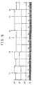
- Fig. 9 is a view which illustrates an example of transition of the switch signals p1 and p2.
- the data of the switch signals p1 and p2 are, together with the obtained x and y-coordinate data, supplied to the data processing unit 7.
- the switch signals p1 and p2 representing the frequency of the AC signal are "00" or "01” at the time of obtaining the reception signal
- the frequency of the switch signal that is, the frequency of the AC signal is maintained intact.
- the cycle of detecting the coordinate when the instruction rod 2 or the marker 3 is used is intended to be shortened as possible for the purpose of improving following-up performance.
- the switch signals p1 and p2 representing the frequency of the AC signal are "10" or "11” at the time of obtaining the reception signal, the frequency of the switching signal, that is, the frequency of the AC signal is successively switched.
- the reason for this lies in that two tuning circuits 46 and 47 having individual frequencies are sometimes operated and their coordinates thereby need to be simultaneously detected when the eraser 4 is used.
- the significantly excellent following-up capability is not needed with respect to the marker 3 or the like which writes image.
- the structure may be arranged such that the signals f0 to f3 are always and repeatedly generated regardless of the results of the coordinate detection although the coordinate-detection speed is slightly reduced.
- the control circuit 601 resets the above-described quadrual counter (step sp1), transmits the thus-obtained counter data, that is, the switch signals p1 and p2 with the start pulse p3 to the signal generating circuit 602 (step sp2), transmits information for selecting x-direction to the XY switch circuit 605 and the transmission and reception switch circuit 606, transmits information for selecting the first loop coil 11x-1 from the x-direction loop coils from 11x-1 to 11x-48 in the sensing portion 11 to the selection circuit 603x, and connects the thus-selected loop coil 11x-1 to the transmission and reception switch circuit 604x.
- the transmission and reception switch circuit 604x alternately connects the loop coil 11x-1 to the drive circuit 610 and the amplifier 61 in response to the above-described transmission and reception switch signal B.
- the drive circuit 610 transmits 16 sine wave signals of 600 kHz as shown in Fig. 11A to the loop coil 11x-1 during the signal reception time period of substantially 27 »sec.
- the above-described switching between signal transmission and signal reception are, as shown in Fig. 11B, repeated 7 times for one loop coil, where it is 11x-1.
- the time period in which the signal transmission and signal reception are repeated 7 times corresponds to the selection period for one loop coil.
- an induced voltage can be obtained at the output of the amplifier 612 for one loop coil every reception time period of 7 times.
- the thus-obtained induced voltages are, as described above, transmitted to the band-pass filter 607 via the reception timing switch circuit 606, wherein the same is averaged and then is transmitted to the control circuit 601 via the detector 608 and the low-pass filter 609.
- the control circuit 601 inputs the output value from the above-described low-pass filter 609 after A/D converting the same as to store the same as the detected voltage related to the distance between the writing tool or the like and the loop coil 11x-1, for example as Vx1.
- the control circuit 601 transmits information for selecting the loop coil 11x-2 to the selection circuit 603x, connects this loop coil 11x-2 to the transmission and reception switch circuit 604x, obtains and stores the detection voltage Vx2 relating to the distance between the writing tool or the like and the loop coil 11x-2, successively and similarly connects the loop coils 11x-3 to 11x-48 to the transmission and reception switch circuit 604x, and stores the detection voltages Vx1 to Vx48 (however, Fig. 11C illustrates only a part of the voltages in an analog-like manner) relating to each of the distances between each of the loop coils as shown in Fig. 11C and the writing tool or the like in x-direction (step sp3).
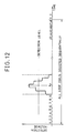
- the practical detected voltages are, as shown in Fig. 12, obtained in several loop coils centering the position (xp) of the writing tool.
- control circuit 601 transmits y-direction selection information to the XY switch circuit 605 and the reception timing switch circuit 606, similarly switches the selection circuit 603y and the transmission and reception switch circuit 604y, and temporally stores the detected voltage relating to each of the distances between the writing tool or the like and each of the loop coils 11y-1 to 11y-30 in y-direction and obtained by A/D-converting the output value from the low-pass filter 609 (step sp4).
- control circuit 601 determines whether or not the level of the detected voltage which has been stored exceeds a predetermined level (step sp5). If it is below the predetermined level, the quadrual counter is stepped by "1" (step sp6), and the above-described steps sp2 to sp5 are repeated.
- step sp7 If the same exceeds the predetermined level, the x and y-coordinates of the writing tool or the like are calculated from the thus-stored voltage level in a manner to be described later (step sp7), transmits the thus-calculated coordinates with the switch signals p1 and p2 to the data processing unit 7 (step sp8), and determines whether or not the switching signals p1 and p2 is "00" or "01” at this time (step sp9). If the same are "00" or "01”, the process according to steps sp2 to sp9 are repeated with the quadrual counter maintained intact. If the same are "10” or "11”, the quadrual counter is stepped by "1” (step sp6), and the processes according to steps sp2 to sp9 are repeated.
- the above-described coordinate xp As a method for calculating the x or y-coordinate, for example, the above-described coordinate xp, there is a method in which the waveforms in the vicinity of the maximal values of the above-described detected voltages Vx1 to Vx48 are approximated by an appropriate function and the coordinates of the maximal value of this function are calculated.
- xp x2 + Dx/2 ⁇ 3Vx2 - 4Vx3 + Vx4)/(Vx2-2Vx3 + Vx4) ⁇
- the coordinate xp of the writing tool or the like can be calculated by performing the calculation expressed in Equation (6) by using the detected voltage of the maximal value and the detected voltages in the vicinity of this maximal value which have been obtained at the above-described level check extracted from the detected voltages Vx1 to Vx48 and the coordinates (known) of the loop coil which is disposed forward by one from the loop coil at which the detected voltage of the above-described maximal value has been obtained.
- Fig. 13 is a view which illustrates the structure of the data processing unit 7, wherein reference numeral 71 represents a microprocessor (CPU), 72 represents a frame memory, 73 represents a overlay memory, 74, 75, 76, and 77 represent interface circuits which respectively corresponds to the operation switch 51, sensing portion control unit 6, printer 8, and display (omitted from illustration).
- reference numeral 71 represents a microprocessor (CPU)
- 72 represents a frame memory
- 73 represents a overlay memory
- 74, 75, 76, and 77 represent interface circuits which respectively corresponds to the operation switch 51, sensing portion control unit 6, printer 8, and display (omitted from illustration).
- Fig. 14 is a flow chart which illustrates the program relating to processing of image information in the data processing unit 7.
- Image information processing means is formed by this program and the microprocessor 71.
- the microprocessor 71 receives data comprising the x and y-coordinates and the identification information from the sensing portion control unit 6 via the interface circuit 75 (step s1), and determines whether or not the thus-received information is "00" (step s2).
- the microprocessor 71 determines that the coordinates at this time are temporal positional data, and causes the character generator (omitted from illustration) to generate a cursor pattern ,for example, an arrow " ⁇ " as to be written in an address in the overlay memory 73 which corresponds to the above-described coordinates (step s3). Since the contents of the overlay memory 73 can be lost if no data is written within a predetermined time period (usually several ms), the above-described address in which the cursor has been written is changed in accordance with the change of the coordinates transmitted from the sensing portion control unit 6.
- step s4 If the identification information is not "00”, it is determined whether or not the same is "01" (step s4). If the identification information is "01”, it is determined that the data corresponds to the image drawn on the writing surface 14 by the marker 3 so that bit "1" is written in the address in the frame memory 72 corresponding to the above-described coordinates (step s5). Contents written in the frame memory 72 can be retained if no other data is written therein.
- the data is the data for determining a predetermined range on the writing surface 14 to be erased by the eraser 4 so that bit "0" is written in the address in the frame memory 72 corresponding to the predetermined range to be erased and determined by the above-described coordinates (step s6), and the image information is deleted.
- the microprocessor 71 transmits the contents of the frame memory 73 to the printer 8 via the interface circuit 76 so that these contents are subjected to a hard copying process.
- the microprocessor 71 When a display device is connected, the microprocessor 71 simultaneously reads out the contents of the frame memory 72 and the overlay memory 73 via the interface circuit 77 and simultaneously converts the contents to a video signal as to be transmitted to and displayed on the display device.
- the contents of the frame memory 72 are rewritten in accordance with the coordinates at that time.
- the instruction rod 2 is used on the writing surface 14, or when the marker 3 is used such that the same does not come contact with the writing surface 14, the cursor is written in the overlay memory 73 in accordance with the coordinates at that time. Therefore, image corresponding to the image written on the writing surface 14 is displayed by dots on the frame of the display device, and the position of the instruction rod 2 or the marker 3 pointing an optional position on the writing surface 14 is indicated by the cursor.
- data received from the sensing portion control unit 6 can be transmitted to the other electronic blackboard connected by means of an interface circuit, a MODEM and communication lines for the purpose of display the similar image or cursor on the display device of the other electronic blackboard.
- a multiplicity of markers comprising the other color felt pens, for example, red, blue and so on and tuning circuits each of which having individual frequencies may be prepared, these markers being identified from the above-described identification information as to be processed on frame memories corresponding to the multiplicity of colors.
- Fig. 15 is a view which illustrates a second embodiment of the electronic blackboard according to the present invention, in which an example of a structure in which two writing surfaces are provided is illustrated.
- reference numeral 15 represents a frame supported as to be rotatable with respect to the legs 16 with a support shaft 17.
- Each of the obverse side and the reverse side of this frame 15 can be optionally made face the direction of the surface of this drawing sheet.
- the frame 15 is, as shown in Fig. 16, provided with, on both sides of the sensing portion 11 thereof, honeycomb members 151 and 152 made of a non-metallic material such as a synthetic resin or the like, and boards 153 and 154 which are similarly made of a non-metallic material are disposed on both sides of the above-described honeycomb members 151 and 152.
- the boards 153 and 154 respectively have corresponding writing surface 18 and 19 which can be repeatedly used.
- the frame 15 and the legs 16 respectively includes couplers 91, 92, and 93 for the purpose of transmitting information therebetween.
- These couplers 91 to 93 are arranged such that when either of the two writing surfaces, for example, the writing surface 18 is made face the surface of this drawing sheet, the couplers 91 and 92 confront each other, while when the other one, that is, the writing surface 19 is made face the surface of this drawing sheet, the couplers 91 and 93 confront each other.
- couplers 91 to 93 include, for example, light emitting diodes or phototransistors for the purpose of transmitting information by means of optical signals.
- the sensing portion control unit 6 is disposed within the frame 15 (for example, in the circumferential portion of the sensing portion 11) so that information to be transmitted by means of the couplers 91 to 93 becomes the above-described coordinates or identification information.
- a metallic member 94 and non-contact sensors 95 and 96 are respectively disposed adjacent to the above-described positions at which the couplers 91 to 93 are positioned in the frame 15 and the legs 16 so that when the writing surface 18 is made face the surface of this drawing sheet, the metallic member 94 and the non-contact sensor 95 confront each other, while when the other one, that is, the writing surface 19 is made face the surface of this drawing sheet, the metallic member 94 and the non-contact sensor 96 confront each other so that detection of the fact which one of the writing surfaces 18 and 19 is being positioned to face the surface of this drawing sheet can be readily performed, that is, a fact that which one is being used can be readily detected.
- the outputs from the non-contact sensors 95 and 96 are transmitted to the data processing unit 7 via an interface circuit (omitted from illustration).
- the power for the sensing portion control unit 6 in the frame 16 is arranged to be supplied through a mechanical and electric contact (omitted from illustration) disposed similarly to the couplers 91 to 93.
- the vertical positions of the sensing portions 11 are made inverse between the case in which the writing surface 18 is made to face the surface of this drawing sheet and the case in which the writing surface 19 is made to face the same. Therefore, even if the same image has been written, coordinates whose vertical positions are different are output from the sensing portion control unit 6.
- Fig. 17 is a flow chart of a program employed in the data processing unit 7 according to the present invention.
- a fact that which one of the writing surface of the frame 15 faces the surface of this drawing sheet is detected on the basis of the outputs from the non-contact sensors 95 and 96 (step s7) and the vertical coordinate, for example, y-coordinate is used intact or is converted into a value obtained by subtracting this coordinate from the maximal value in the subject direction (step s8). Therefore, according to the present invention, both of the writing surfaces can be used in the same manner regardless of consciousness of recognizing the writing surface.
- the metallic member 94 and the non-contact sensor 95 and 96 form means for detecting the writing surface which is being used, while, the program and microprocessor 71 shown in Fig. 17 form coordinate conversion means.
- the sensing portion described in the first and second embodiments is usually formed by an insulating substrate having a printed conductive pattern as to correspond to the positions of the above-described x and y-direction loop coils.
- a structure may be employed which is arranged such that a member in which a multiplicity of conductive wires are, at predetermined intervals, held between two insulating films and the thus-held conductive wires are connected to each other so as to correspond to the positions of the x and y-direction loop coils.
- the loop coil for generating the electric wave and the loop coil for detecting the electric wave may be individually provided.
- the structure may be arranged to always generate the electric wave.
- a structure may be formed such that a transmitting sensing portion and a receiving sensing portion may be individually provided. It is not necessarily critical for the transmission and the reception to be subjected to the time-division treatment. For example, a structure may be arranged such that the transmission side continues the transmission and the reception side detects a predetermined electric wave from the transmission side by switching only the coils of the turning circuit.
Landscapes
- Engineering & Computer Science (AREA)
- General Engineering & Computer Science (AREA)
- Theoretical Computer Science (AREA)
- Physics & Mathematics (AREA)
- Human Computer Interaction (AREA)
- General Physics & Mathematics (AREA)
- Electromagnetism (AREA)
- Position Input By Displaying (AREA)
- Drawing Aids And Blackboards (AREA)
- Facsimiles In General (AREA)
Claims (11)
- Dispositif de tableau électronique, comprenant:
un outil d'écriture (3) ayant un instrument d'écriture tel qu'un stylo feutre (32) et un premier circuit d'accord (33) qui comprend au moins une bobine (332) et un condensateur (333,334), ledit circuit d'accord ayant une première fréquence d'accord prédéterminée (f1),
un effaceur (4) ayant un moyen d'effacement (45) apte à effacer des caractères ou autres écrits avec ledit instrument d'écriture, ledit effaceur ayant au moins un deuxième circuit d'accord (46,47) comprenant au moins une bobine (463,467) et un condensateur (462,472) et ayant une deuxième fréquence d'accord prédéterminée (f2,f3),
un corps (1) de tableau ayant une surface d'écriture sur laquelle des écritures/effacements répétés sont possibles avec ledit outil d'écriture (3) et ledit effaceur (4),
une partie de détection (11) placée dans ledit corps de tableau à proximité immédiate de ladite surface d'écriture et comportant un moyen (11x,11y,610,611) de production d'ondes électriques apte à produire des ondes électriques pour exciter au moins un desdits circuits d'accord, et un moyen (11x,11y,612,613) de détection d'ondes électriques apte à détecter des ondes électriques produites à partir du circuit d'accord qui a été excité,
un moyen de détection de coordonnées pour déterminer des valeurs de coordonnées pour la position dudit outil d'écriture (3) ou dudit effaceur (4) par rapport à ladite surface d'écriture, en fonction de la fréquence des ondes électriques détectées par ledit moyen de détection d'ondes électriques, et
un moyen d'identification pour identifier lequel desdits outil d'écriture et effaceur est utilisé sur la surface d'écriture, en fonction de la fréquence de l'onde électrique détectée par ledit moyen de détection d'onde électrique. - Dispositif de tableau électronique selon la revendication 1, dans lequel un moyen (7) de traitement d'informations d'image est présent pour traiter des informations d'image à sortir sur un dispositif (8) de sortie en fonction des informations de coordonnées détectées par ledit moyen de détection de coordonnées, pour représenter de ce fait les informations d'image entrées à l'aide de l'outil d'écriture (3) et éliminer les informations d'image effacées à l'aide dudit effaceur (4).
- Dispositif de tableau électronique selon la revendication 1 ou 2, dans lequel ledit moyen de production d'ondes électriques et ledit moyen de détection d'ondes électriques sont conçus pour fonctionner en alternance.
- Dispositif de tableau électronique selon l'une quelconque des revendications 1 à 3, dans lequel ledit moyen de production d'ondes électriques et ledit moyen de détection d'ondes électriques comprennent des groupes (11x-1... 11x-48; 11y-1... 11y-30) d'enroulements en boucle dans les sens x et y, lesdits groupes d'enroulements en boucle étant communs au moyen de production d'ondes électriques et au moyen de détection d'ondes électriques.
- Dispositif de tableau électronique selon l'une quelconque des revendications précédentes, dans lequel ledit outil d'écriture (4) comporte un moyen (331) pour modifier la fréquence d'accord du circuit d'accord (33) de celui-ci entre une pluralité de fréquences d'accord prédéterminées (f0, f1) que ledits moyens et production et de détection d'ondes électriques sont aptes à émettre et à détecter.
- Dispositif de tableau électronique selon l'une quelconque des revendications précédentes, comprenant:
deux surfaces d'écriture (153,154) disposées de part et d'autre de ladite partie de détection et aptes à être utilisées de manière répétée,
un moyen (94,95,96) pour déterminer laquelle des deux surfaces d'écriture est en train d'être utilisée, et
un moyen de conversion de coordonnées pour convertir les valeurs de coordonnées détectées par ledit moyen de détection de coordonnées selon celle des surfaces d'écriture qui est en train d'être utilisée. - Baguette d'instruction (2) utilisable avec un dispositif de tableau électronique selon l'une quelconque des revendications précédentes, comportant un corps (21) analogue à une baguette qui a une longueur prédéterminée au moins pendant son utilisation et dont l'extrémité antérieure renferme un circuit d'accord ayant une fréquence d'accord prédéterminée (f0) que lesdits moyens de production et de détection d'ondes électriques sont aptes à émettre et à détecter.
- Marqueur (3) utilisable comme outil d'écriture dans un dispositif de tableau électronique selon l'une quelconque des revendications 1 à 6, comprenant une enveloppe (31) logeant un corps (32) de crayon en tant qu'instrument d'écriture, et un circuit d'accord (33) constitué au moins par une bobine (332) comprenant un noyau et un condensateur (333, 334), dans lequel une partie dudit corps de crayon dépasse ou peut dépasser de la surface extérieure de ladite enveloppe pour permettre l'écriture sur ladite surface d'écriture, et ledit circuit d'accord peut être excité par des ondes électriques émises depuis ledit moyen de production d'ondes électriques et réémet des ondes électriques vers ledit moyen de détection d'ondes électriques de façon que l'écriture à l'aide dudit corps de crayon soit autorisée et que la position de coordonnées du marqueur soit appliquée à la partie de détection (11).
- Marqueur selon la revendication 8, dans lequel ledit corps de crayon comprend un stylo feutre utilisable sur un tableau blanc habituel et disponible sur le marché.
- Marqueur selon la revendication 8 ou 9, dans lequel ladite enveloppe est constituée par au moins deux pièces séparables (31a,31b) de façon à permettre le remplacement dudit corps de crayon.
- Effaceur (4) utilisable dans un dispositif de tableau électronique selon l'une quelconque des revendications 1 à 6, dans lequel le moyen d'effacement (45) est conçu pour avoir une surface prédéterminée et au moins deux circuits d'accord sont disposés à des extrémités opposées de ladite surface.
Applications Claiming Priority (2)
| Application Number | Priority Date | Filing Date | Title |
|---|---|---|---|
| JP154518/88 | 1988-06-22 | ||
| JP63154518A JPH01320521A (ja) | 1988-06-22 | 1988-06-22 | 電子黒板装置及びその筆記具等 |
Publications (3)
| Publication Number | Publication Date |
|---|---|
| EP0347725A2 EP0347725A2 (fr) | 1989-12-27 |
| EP0347725A3 EP0347725A3 (en) | 1990-09-05 |
| EP0347725B1 true EP0347725B1 (fr) | 1995-02-01 |
Family
ID=15586004
Family Applications (1)
| Application Number | Title | Priority Date | Filing Date |
|---|---|---|---|
| EP89110724A Expired - Lifetime EP0347725B1 (fr) | 1988-06-22 | 1989-06-13 | Tableau élctronique et accessoires tels que les instruments d'écriture |
Country Status (6)
| Country | Link |
|---|---|
| US (2) | US5023408A (fr) |
| EP (1) | EP0347725B1 (fr) |
| JP (1) | JPH01320521A (fr) |
| KR (1) | KR0133068B1 (fr) |
| CN (1) | CN1024853C (fr) |
| DE (1) | DE68920916T2 (fr) |
Cited By (9)
| Publication number | Priority date | Publication date | Assignee | Title |
|---|---|---|---|---|
| US8115753B2 (en) | 2007-04-11 | 2012-02-14 | Next Holdings Limited | Touch screen system with hover and click input methods |
| US8149221B2 (en) | 2004-05-07 | 2012-04-03 | Next Holdings Limited | Touch panel display system with illumination and detection provided from a single edge |
| US8289299B2 (en) | 2003-02-14 | 2012-10-16 | Next Holdings Limited | Touch screen signal processing |
| US8384693B2 (en) | 2007-08-30 | 2013-02-26 | Next Holdings Limited | Low profile touch panel systems |
| US8405637B2 (en) | 2008-01-07 | 2013-03-26 | Next Holdings Limited | Optical position sensing system and optical position sensor assembly with convex imaging window |
| US8432377B2 (en) | 2007-08-30 | 2013-04-30 | Next Holdings Limited | Optical touchscreen with improved illumination |
| US8456447B2 (en) | 2003-02-14 | 2013-06-04 | Next Holdings Limited | Touch screen signal processing |
| US8508508B2 (en) | 2003-02-14 | 2013-08-13 | Next Holdings Limited | Touch screen signal processing with single-point calibration |
| US8692768B2 (en) | 2009-07-10 | 2014-04-08 | Smart Technologies Ulc | Interactive input system |
Families Citing this family (138)
| Publication number | Priority date | Publication date | Assignee | Title |
|---|---|---|---|---|
| JP2971488B2 (ja) * | 1989-11-01 | 1999-11-08 | 株式会社ワコム | 位置検出装置 |
| JPH0542510Y2 (fr) * | 1990-01-30 | 1993-10-26 | ||
| JPH048137U (fr) * | 1990-05-07 | 1992-01-24 | ||
| US5025314A (en) * | 1990-07-30 | 1991-06-18 | Xerox Corporation | Apparatus allowing remote interactive use of a plurality of writing surfaces |
| CA2051204C (fr) * | 1990-11-02 | 1999-04-20 | Scott A. Elrod | Systeme de saisie de donnees de position et de fonction pour afficheur a grande surface |
| EP0535442B1 (fr) * | 1991-10-04 | 1995-12-27 | Bernd Dipl-Ing. Dölling | Dispositif pour la production de dessins sur un support en forme de feuille, par exemple sur une feuille en papier transparent, au moyen d'un outil générant des points, traits, tel que crayon ou compas |
| US6141000A (en) | 1991-10-21 | 2000-10-31 | Smart Technologies Inc. | Projection display system with touch sensing on screen, computer assisted alignment correction and network conferencing |
| CA2058219C (fr) * | 1991-10-21 | 2002-04-02 | Smart Technologies Inc. | Systeme d'affichage interactif |
| EP0549956B1 (fr) * | 1991-12-26 | 1998-03-18 | Seiko Instruments Inc. | Système de lecture de coordonnées pour détecter les états d'opération d'interrupteurs nombreux |
| JPH0792722B2 (ja) * | 1992-02-21 | 1995-10-09 | グラフテック株式会社 | デジタイザ |
| JPH0619615A (ja) * | 1992-06-29 | 1994-01-28 | Matsushita Electric Ind Co Ltd | 手書き文字入力装置 |
| US5248856A (en) * | 1992-10-07 | 1993-09-28 | Microfield Graphics, Inc. | Code-based, electromagnetic-field-responsive graphic data-acquisition system |
| GB2273778A (en) † | 1992-12-22 | 1994-06-29 | Tds Cad Graphics Limited | Cordless digitizer |
| US5619253A (en) * | 1993-06-25 | 1997-04-08 | Miranda, Jr.; Henry A. | Video display of indicia |
| US5583323A (en) * | 1993-11-05 | 1996-12-10 | Microfield Graphics, Inc. | Calibration of graphic data-acquisition tracking system |
| US5434370A (en) * | 1993-11-05 | 1995-07-18 | Microfield Graphics, Inc. | Marking system with pen-up/pen-down tracking |
| US5585605A (en) * | 1993-11-05 | 1996-12-17 | Microfield Graphics, Inc. | Optical-scanning system employing laser and laser safety control |
| JPH07225644A (ja) * | 1994-02-10 | 1995-08-22 | Wacom Co Ltd | 位置指示器 |
| US5714720A (en) * | 1994-09-15 | 1998-02-03 | Calcomp Inc. | High efficiency passive pointer digitizer system |
| JP3015269B2 (ja) * | 1994-12-05 | 2000-03-06 | 株式会社ワコム | 位置検出装置及びその方法 |
| FI103837B (fi) * | 1994-12-22 | 1999-09-30 | Nokia Mobile Phones Ltd | Tiedonsiirto- ja käsittelymenetelmä |
| US5594215A (en) * | 1995-01-20 | 1997-01-14 | Jeng; James H. | Wireless digitizer and stylus pen unit |
| GB2339662B (en) * | 1995-05-05 | 2000-04-12 | Wacom Co Ltd | Digitizer eraser system and method |
| JPH09106320A (ja) * | 1995-08-24 | 1997-04-22 | Symbios Logic Inc | 図形入力装置および図形入力方法 |
| US6730862B1 (en) * | 1995-12-27 | 2004-05-04 | Lsi Logic Corporation | Erase feature in pen-based computing |
| US5823782A (en) | 1995-12-29 | 1998-10-20 | Tinkers & Chance | Character recognition educational system |
| US6167353A (en) * | 1996-07-03 | 2000-12-26 | Interval Research Corporation | Computer method and apparatus for interacting with a physical system |
| US6445384B1 (en) * | 1996-10-01 | 2002-09-03 | Greensteel, Inc. | Electronic whiteboard system eraser |
| US6353193B1 (en) * | 1996-10-01 | 2002-03-05 | Greensteel, Inc. | Electronic whiteboard system and method |
| JPH10109494A (ja) * | 1996-10-08 | 1998-04-28 | Matsushita Electric Ind Co Ltd | 電子黒板装置 |
| US6067080A (en) | 1997-02-21 | 2000-05-23 | Electronics For Imaging | Retrofittable apparatus for converting a substantially planar surface into an electronic data capture device |
| US6326565B1 (en) | 1997-02-28 | 2001-12-04 | Electronics For Imaging, Inc. | Marking device for electronic presentation board |
| US5866856A (en) * | 1997-02-28 | 1999-02-02 | Electronics For Imaging, Inc. | Marking device for electronic presentation board |
| IL120417A (en) * | 1997-03-10 | 2000-09-28 | Electronics For Imaging Inc | Presentation board digitizer systems |
| US6292177B1 (en) | 1997-03-05 | 2001-09-18 | Tidenet, Inc. | Marking device for electronic presentation board |
| US6188493B1 (en) * | 1997-04-18 | 2001-02-13 | Matsushita Electric Industrial Co., Ltd. | Electronic blackboard device |
| US6442213B1 (en) * | 1997-04-22 | 2002-08-27 | Silicon Laboratories Inc. | Digital isolation system with hybrid circuit in ADC calibration loop |
| US6104387A (en) * | 1997-05-14 | 2000-08-15 | Virtual Ink Corporation | Transcription system |
| JP3933278B2 (ja) * | 1997-11-04 | 2007-06-20 | 株式会社ワコム | 位置指示器を検出可能な位置検出方法及び装置 |
| US6151014A (en) * | 1998-02-26 | 2000-11-21 | Pagasus Technologies Ltd. | Systems and processing algorithms for ultrasound time-of-flight digitizer systems |
| US6356255B1 (en) * | 1998-04-07 | 2002-03-12 | Interval Research Corporation | Methods and systems for providing programmable computerized interactors |
| US6025783A (en) * | 1998-04-30 | 2000-02-15 | Trw Vehicle Safety Systems Inc. | Wireless switch detection system |
| US6177927B1 (en) | 1998-05-14 | 2001-01-23 | Virtual Ink Corp. | Transcription system kit |
| US6100877A (en) * | 1998-05-14 | 2000-08-08 | Virtual Ink, Corp. | Method for calibrating a transcription system |
| US6211863B1 (en) | 1998-05-14 | 2001-04-03 | Virtual Ink. Corp. | Method and software for enabling use of transcription system as a mouse |
| US6124847A (en) * | 1998-05-14 | 2000-09-26 | Virtual Ink, Corp. | Collapsible detector assembly |
| US6191778B1 (en) | 1998-05-14 | 2001-02-20 | Virtual Ink Corp. | Transcription system kit for forming composite images |
| US6147681A (en) * | 1998-05-14 | 2000-11-14 | Virtual Ink, Corp. | Detector for use in a transcription system |
| US6111565A (en) * | 1998-05-14 | 2000-08-29 | Virtual Ink Corp. | Stylus for use with transcription system |
| US6232962B1 (en) | 1998-05-14 | 2001-05-15 | Virtual Ink Corporation | Detector assembly for use in a transcription system |
| US6396005B2 (en) | 1998-06-15 | 2002-05-28 | Rodgers Technology Center, Inc. | Method and apparatus for diminishing grid complexity in a tablet |
| JP2000043484A (ja) * | 1998-07-30 | 2000-02-15 | Ricoh Co Ltd | 電子黒板システム |
| US6335724B1 (en) * | 1999-01-29 | 2002-01-01 | Ricoh Company, Ltd. | Method and device for inputting coordinate-position and a display board system |
| US7971784B2 (en) * | 1999-05-25 | 2011-07-05 | Silverbrook Research Pty Ltd | Sensing device with mode changes via nib switch |
| US7721948B1 (en) | 1999-05-25 | 2010-05-25 | Silverbrook Research Pty Ltd | Method and system for online payments |
| US20070143715A1 (en) * | 1999-05-25 | 2007-06-21 | Silverbrook Research Pty Ltd | Method of providing information via printed substrate and gesture recognition |
| US7762453B2 (en) | 1999-05-25 | 2010-07-27 | Silverbrook Research Pty Ltd | Method of providing information via a printed substrate with every interaction |
| US7593899B1 (en) | 1999-05-25 | 2009-09-22 | Silverbrook Research Pty Ltd | Method and system for online payments |
| US20070233513A1 (en) * | 1999-05-25 | 2007-10-04 | Silverbrook Research Pty Ltd | Method of providing merchant resource or merchant hyperlink to a user |
| US7832626B2 (en) * | 1999-05-25 | 2010-11-16 | Silverbrook Research Pty Ltd | Anonymous competition entry |
| US7857201B2 (en) * | 1999-05-25 | 2010-12-28 | Silverbrook Research Pty Ltd | Method and system for selection |
| US7760969B2 (en) * | 1999-05-25 | 2010-07-20 | Silverbrook Research Pty Ltd | Method of providing information via context searching from a printed substrate |
| US8113950B2 (en) | 1999-05-25 | 2012-02-14 | Silverbrook Research Pty Ltd | Competition entry with limited return messaging |
| US7793824B2 (en) | 1999-05-25 | 2010-09-14 | Silverbrook Research Pty Ltd | System for enabling access to information |
| JP4052498B2 (ja) | 1999-10-29 | 2008-02-27 | 株式会社リコー | 座標入力装置および方法 |
| EP1261895B1 (fr) * | 1999-12-10 | 2005-11-23 | Sensopad Limited | Interface homme-machine |
| JP2001184161A (ja) | 1999-12-27 | 2001-07-06 | Ricoh Co Ltd | 情報入力方法、情報入力装置、筆記入力装置、筆記データ管理方法、表示制御方法、携帯型電子筆記装置および記録媒体 |
| US20020054026A1 (en) * | 2000-04-17 | 2002-05-09 | Bradley Stevenson | Synchronized transmission of recorded writing data with audio |
| US6803906B1 (en) | 2000-07-05 | 2004-10-12 | Smart Technologies, Inc. | Passive touch system and method of detecting user input |
| ATE453147T1 (de) | 2000-07-05 | 2010-01-15 | Smart Technologies Ulc | Verfahren für ein kamerabasiertes berührungssystem |
| WO2002043045A1 (fr) * | 2000-11-22 | 2002-05-30 | Cirque Corporation | Dispositif d'entree de stylet a aimant permanent |
| JP2002163070A (ja) * | 2000-11-27 | 2002-06-07 | Matsushita Electric Ind Co Ltd | 電子黒板 |
| US7511705B2 (en) * | 2001-05-21 | 2009-03-31 | Synaptics (Uk) Limited | Position sensor |
| US7196604B2 (en) * | 2001-05-30 | 2007-03-27 | Tt Electronics Technology Limited | Sensing apparatus and method |
| GB0126014D0 (en) * | 2001-10-30 | 2001-12-19 | Sensopad Technologies Ltd | Modulated field position sensor |
| US7126590B2 (en) * | 2001-10-04 | 2006-10-24 | Intel Corporation | Using RF identification tags in writing instruments as a means for line style differentiation |
| US20030095115A1 (en) * | 2001-11-22 | 2003-05-22 | Taylor Brian | Stylus input device utilizing a permanent magnet |
| CN2512043Y (zh) * | 2001-12-29 | 2002-09-18 | 台均实业有限公司 | 具有柔性隔膜式电磁感应发生装置的电子白板 |
| US7486270B2 (en) * | 2001-12-29 | 2009-02-03 | Tai Guen Enterprise Co., Ltd. | Electromagnetic induction electronic board with antenna arrayed in gridding inside |
| GB2403017A (en) * | 2002-03-05 | 2004-12-22 | Synaptics | Position sensor |
| US7224347B2 (en) * | 2002-05-09 | 2007-05-29 | Hewlett-Packard Development Company, L.P. | Writeboard method and apparatus |
| US6875933B2 (en) | 2002-05-10 | 2005-04-05 | Luidia Inc. | Methods and apparatus for configuring a writing surface |
| US20040070616A1 (en) * | 2002-06-02 | 2004-04-15 | Hildebrandt Peter W. | Electronic whiteboard |
| US7427983B1 (en) * | 2002-06-02 | 2008-09-23 | Steelcase Development Corporation | Visual communication system |
| EP1509833A2 (fr) * | 2002-06-05 | 2005-03-02 | Synaptics (UK) Limited | Procede et appareil de transfert de signal |
| CN100553513C (zh) | 2002-07-31 | 2009-10-28 | 株式会社钟化 | 人造头发用纤维及其制造方法 |
| CN1242319C (zh) * | 2002-09-17 | 2006-02-15 | 台均实业股份有限公司 | 内置导线网格电磁感应层的电子白板 |
| US20040063078A1 (en) * | 2002-09-30 | 2004-04-01 | Marcus Brian I. | Electronic educational toy appliance |
| GB2394293A (en) * | 2002-10-16 | 2004-04-21 | Gentech Invest Group Ag | Inductive sensing apparatus and method |
| WO2004036147A2 (fr) * | 2002-10-16 | 2004-04-29 | Tt Electronics Technology Limited | Appareil de detection et procede associe |
| US6954197B2 (en) | 2002-11-15 | 2005-10-11 | Smart Technologies Inc. | Size/scale and orientation determination of a pointer in a camera-based touch system |
| GB0303627D0 (en) * | 2003-02-17 | 2003-03-19 | Sensopad Technologies Ltd | Sensing method and apparatus |
| US7532206B2 (en) * | 2003-03-11 | 2009-05-12 | Smart Technologies Ulc | System and method for differentiating between pointers used to contact touch surface |
| GB0317370D0 (en) * | 2003-07-24 | 2003-08-27 | Synaptics Uk Ltd | Magnetic calibration array |
| GB0319945D0 (en) * | 2003-08-26 | 2003-09-24 | Synaptics Uk Ltd | Inductive sensing system |
| EP1668451A4 (fr) * | 2003-09-12 | 2007-07-04 | Cirque Corp | Stylet attache s'utilisant avec un pave tactile sensible a la capacitance |
| US7411575B2 (en) | 2003-09-16 | 2008-08-12 | Smart Technologies Ulc | Gesture recognition method and touch system incorporating the same |
| US7274356B2 (en) | 2003-10-09 | 2007-09-25 | Smart Technologies Inc. | Apparatus for determining the location of a pointer within a region of interest |
| US7355593B2 (en) | 2004-01-02 | 2008-04-08 | Smart Technologies, Inc. | Pointer tracking across multiple overlapping coordinate input sub-regions defining a generally contiguous input region |
| US20050156952A1 (en) * | 2004-01-20 | 2005-07-21 | Orner Edward E. | Interactive display systems |
| WO2005096772A2 (fr) | 2004-04-01 | 2005-10-20 | Finepoint Innovations, Inc. | Systeme transducteur de surface sans fil |
| US7460110B2 (en) | 2004-04-29 | 2008-12-02 | Smart Technologies Ulc | Dual mode touch system |
| US8120596B2 (en) | 2004-05-21 | 2012-02-21 | Smart Technologies Ulc | Tiled touch system |
| JP2008509418A (ja) * | 2004-08-09 | 2008-03-27 | センソパッド リミテッド | 検知装置及び検知方法 |
| TWI266530B (en) * | 2005-07-29 | 2006-11-11 | Coretronic Corp | Projector |
| US7883420B2 (en) | 2005-09-12 | 2011-02-08 | Mattel, Inc. | Video game systems |
| KR100833365B1 (ko) * | 2006-02-23 | 2008-05-28 | 엘지전자 주식회사 | 리모콘과 그를 이용한 영상표시장치 |
| US9442607B2 (en) | 2006-12-04 | 2016-09-13 | Smart Technologies Inc. | Interactive input system and method |
| EP2145158B1 (fr) | 2007-05-10 | 2018-03-07 | Cambridge Integrated Circuits Limited | Transducteur |
| US8094137B2 (en) | 2007-07-23 | 2012-01-10 | Smart Technologies Ulc | System and method of detecting contact on a display |
| CN201112112Y (zh) * | 2007-09-28 | 2008-09-10 | 深圳市浦天利光电技术有限公司 | 一种高频大功率平板变压器 |
| US8902193B2 (en) | 2008-05-09 | 2014-12-02 | Smart Technologies Ulc | Interactive input system and bezel therefor |
| US8243028B2 (en) * | 2008-06-13 | 2012-08-14 | Polyvision Corporation | Eraser assemblies and methods of manufacturing same |
| US8890842B2 (en) | 2008-06-13 | 2014-11-18 | Steelcase Inc. | Eraser for use with optical interactive surface |
| CN101685366A (zh) * | 2008-09-26 | 2010-03-31 | 汉王科技股份有限公司 | 具有多点触摸功能的电磁感应装置 |
| US8339378B2 (en) | 2008-11-05 | 2012-12-25 | Smart Technologies Ulc | Interactive input system with multi-angle reflector |
| US8400419B2 (en) * | 2009-04-20 | 2013-03-19 | Broadcom Corporation | Dual mode inductive touch screen for use in a configurable communication device and methods for use therewith |
| JP4535205B2 (ja) * | 2009-10-14 | 2010-09-01 | パナソニック株式会社 | 電子黒板システム |
| GB2488389C (en) | 2010-12-24 | 2018-08-22 | Cambridge Integrated Circuits Ltd | Position sensing transducer |
| CN102736818A (zh) * | 2011-04-12 | 2012-10-17 | 北京瑞麟百嘉科技有限公司 | 一种电磁多笔电子白板 |
| KR20130123691A (ko) * | 2012-05-03 | 2013-11-13 | 삼성전자주식회사 | 터치 입력 방법 및 이를 적용한 터치 디스플레이 장치 |
| GB2503006B (en) | 2012-06-13 | 2017-08-09 | Cambridge Integrated Circuits Ltd | Position sensing transducer |
| US9164595B2 (en) * | 2013-03-08 | 2015-10-20 | Darren C. PETERSEN | Mechanical actuator apparatus for a touchscreen |
| US9158390B2 (en) * | 2013-03-08 | 2015-10-13 | Darren C. PETERSEN | Mechanical actuator apparatus for a touch sensing surface of an electronic device |
| KR102120772B1 (ko) * | 2013-06-28 | 2020-06-17 | 삼성전자주식회사 | 전자칠판용 영상 지우개 디바이스 및 그 제어방법, 디스플레이장치 및 그 제어방법, 전자칠판 시스템 |
| US10180736B2 (en) | 2014-11-26 | 2019-01-15 | Synaptics Incorporated | Pen with inductor |
| US9946391B2 (en) | 2014-11-26 | 2018-04-17 | Synaptics Incorporated | Sensing objects using multiple transmitter frequencies |
| US10088922B2 (en) | 2014-11-26 | 2018-10-02 | Synaptics Incorporated | Smart resonating pen |
| US10698553B2 (en) * | 2016-07-13 | 2020-06-30 | Sharp Kabushiki Kaisha | Writing input device |
| JP6754643B2 (ja) * | 2016-09-02 | 2020-09-16 | 三菱鉛筆株式会社 | 手書き入力装置 |
| JP7012485B2 (ja) * | 2016-12-27 | 2022-01-28 | 株式会社ワコム | 画像情報処理装置および画像情報処理方法 |
| CN106815586A (zh) * | 2017-03-06 | 2017-06-09 | 温州云航信息科技有限公司 | 新型进程单架及其同步装置 |
| JP6960277B2 (ja) * | 2017-08-31 | 2021-11-05 | 三菱鉛筆株式会社 | 電磁誘導タッチペン |
| US20190163292A1 (en) * | 2017-11-28 | 2019-05-30 | Egalax_Empia Technology Inc. | Electronic Board Eraser and Controlling Method Thereof |
| US20210096709A1 (en) * | 2017-11-28 | 2021-04-01 | Egalax_Empia Technology Inc. | Electronic Board Eraser and Controlling Method Thereof for Setting Erasing Area |
| JP2020004103A (ja) * | 2018-06-28 | 2020-01-09 | シャープ株式会社 | 電子ボード |
| US11670972B2 (en) * | 2018-09-24 | 2023-06-06 | Apple Inc. | Electronic device having an inductive charging system |
| CN112912826B (zh) | 2018-11-06 | 2024-07-23 | 三菱铅笔株式会社 | 输入笔和输入笔的制造方法 |
Family Cites Families (15)
| Publication number | Priority date | Publication date | Assignee | Title |
|---|---|---|---|---|
| US2899596A (en) * | 1959-08-11 | Wide band mixing system | ||
| US2812427A (en) * | 1951-06-27 | 1957-11-05 | Alexander F | Passive radio communication system |
| US2899546A (en) * | 1954-05-25 | 1959-08-11 | hollmann | |
| US2958781A (en) * | 1956-03-22 | 1960-11-01 | Marchal Maurice | Radio-physiological method and means |
| US3117277A (en) * | 1957-09-04 | 1964-01-07 | Karl Rath | Passive radio repeater transmission system |
| US3373425A (en) * | 1967-04-14 | 1968-03-12 | Allen L Well | Tunnel diode circuit utilized to control the reply of a passive transponder |
| US4479032A (en) * | 1982-02-08 | 1984-10-23 | Bausch & Lomb Incorporated | Digitizing cursor and coordinate grid system |
| US4672154A (en) * | 1985-04-03 | 1987-06-09 | Kurta Corporation | Low power, high resolution digitizing system with cordless pen/mouse |
| FR2584836B1 (fr) * | 1985-07-09 | 1992-06-19 | Farel Alain | Procede de saisie informatique de donnees graphiques concomitante a leur creation |
| EP0229637A3 (fr) * | 1986-01-09 | 1988-10-05 | Wacom Co., Ltd. | Appareil de tableau électronique |
| JPS634320A (ja) * | 1986-06-24 | 1988-01-09 | Fujitsu Ltd | 描画入出力装置 |
| EP0254297B1 (fr) * | 1986-07-23 | 1994-06-01 | Wacom Company, Ltd. | Système d'entrée de coordonnées |
| JPH07107661B2 (ja) * | 1986-09-08 | 1995-11-15 | 株式会社ワコム | 位置指示器の状態検出方式 |
| JPS6370326A (ja) * | 1986-09-12 | 1988-03-30 | Wacom Co Ltd | 位置検出装置 |
| JP2583509B2 (ja) * | 1987-06-16 | 1997-02-19 | 株式会社 ワコム | 座標入力装置 |
-
1988
- 1988-06-22 JP JP63154518A patent/JPH01320521A/ja active Pending
-
1989
- 1989-06-13 EP EP89110724A patent/EP0347725B1/fr not_active Expired - Lifetime
- 1989-06-13 DE DE68920916T patent/DE68920916T2/de not_active Expired - Fee Related
- 1989-06-13 US US07/365,388 patent/US5023408A/en not_active Ceased
- 1989-06-13 CN CN89106336A patent/CN1024853C/zh not_active Expired - Lifetime
- 1989-06-21 KR KR1019890008598A patent/KR0133068B1/ko not_active IP Right Cessation
-
1993
- 1993-06-10 US US08/074,569 patent/USRE35329E/en not_active Expired - Lifetime
Cited By (11)
| Publication number | Priority date | Publication date | Assignee | Title |
|---|---|---|---|---|
| US8289299B2 (en) | 2003-02-14 | 2012-10-16 | Next Holdings Limited | Touch screen signal processing |
| US8456447B2 (en) | 2003-02-14 | 2013-06-04 | Next Holdings Limited | Touch screen signal processing |
| US8466885B2 (en) | 2003-02-14 | 2013-06-18 | Next Holdings Limited | Touch screen signal processing |
| US8508508B2 (en) | 2003-02-14 | 2013-08-13 | Next Holdings Limited | Touch screen signal processing with single-point calibration |
| US8149221B2 (en) | 2004-05-07 | 2012-04-03 | Next Holdings Limited | Touch panel display system with illumination and detection provided from a single edge |
| US8115753B2 (en) | 2007-04-11 | 2012-02-14 | Next Holdings Limited | Touch screen system with hover and click input methods |
| US8384693B2 (en) | 2007-08-30 | 2013-02-26 | Next Holdings Limited | Low profile touch panel systems |
| US8432377B2 (en) | 2007-08-30 | 2013-04-30 | Next Holdings Limited | Optical touchscreen with improved illumination |
| US8405637B2 (en) | 2008-01-07 | 2013-03-26 | Next Holdings Limited | Optical position sensing system and optical position sensor assembly with convex imaging window |
| US8405636B2 (en) | 2008-01-07 | 2013-03-26 | Next Holdings Limited | Optical position sensing system and optical position sensor assembly |
| US8692768B2 (en) | 2009-07-10 | 2014-04-08 | Smart Technologies Ulc | Interactive input system |
Also Published As
| Publication number | Publication date |
|---|---|
| EP0347725A2 (fr) | 1989-12-27 |
| KR910000390A (ko) | 1991-01-29 |
| DE68920916T2 (de) | 1995-07-06 |
| CN1040279A (zh) | 1990-03-07 |
| USRE35329E (en) | 1996-09-17 |
| DE68920916D1 (de) | 1995-03-16 |
| US5023408A (en) | 1991-06-11 |
| JPH01320521A (ja) | 1989-12-26 |
| EP0347725A3 (en) | 1990-09-05 |
| CN1024853C (zh) | 1994-06-01 |
| KR0133068B1 (ko) | 1998-04-24 |
Similar Documents
| Publication | Publication Date | Title |
|---|---|---|
| EP0347725B1 (fr) | Tableau élctronique et accessoires tels que les instruments d'écriture | |
| EP0295699B1 (fr) | Appareil pour l'introduction de coordonnées | |
| US4711977A (en) | Electronic blackboard apparatus | |
| JP3262297B2 (ja) | 光学式座標入力装置 | |
| US4890096A (en) | Coordinate input device with display | |
| US4988837A (en) | Position detecting device | |
| US5134388A (en) | Electronic blackboard system marker and eraser therefor | |
| EP0307667B1 (fr) | Système pour l'entrée de coordonnées avec un crayon pour l'introduction des données | |
| US4956526A (en) | Digitizer having flat tablet with magnetic shield plate | |
| JP3786464B2 (ja) | 画像消去方法及びスタイラス型電子筆記システム | |
| EP0187372A2 (fr) | Dispositif pour la détection d'une position | |
| US6606087B1 (en) | Coordinate reader | |
| JPS60134325A (ja) | デイスプレイ付座標入力装置 | |
| JP2857539B2 (ja) | コードレスデジタイザ | |
| US20210294493A1 (en) | Position detection apparatus and position detection method | |
| JPH05216581A (ja) | 入力装置 | |
| JP2007121894A (ja) | 印刷物複製装置及び印刷物複製方法 | |
| JPH01289366A (ja) | 画像入力装置及びそのハンドスキャナ | |
| JPH03241415A (ja) | 座標入力装置 | |
| JPH09146683A (ja) | タブレット装置 | |
| JPH02171910A (ja) | 座標入力装置 | |
| JP2618701B2 (ja) | 図形入力装置 | |
| JPH01119818A (ja) | 座標入力装置 | |
| JPH05341902A (ja) | コードレスデジタイザ | |
| JPH01265317A (ja) | 座標読取装置 |
Legal Events
| Date | Code | Title | Description |
|---|---|---|---|
| PUAI | Public reference made under article 153(3) epc to a published international application that has entered the european phase |
Free format text: ORIGINAL CODE: 0009012 |
|
| AK | Designated contracting states |
Kind code of ref document: A2 Designated state(s): DE FR GB IT |
|
| PUAL | Search report despatched |
Free format text: ORIGINAL CODE: 0009013 |
|
| AK | Designated contracting states |
Kind code of ref document: A3 Designated state(s): DE FR GB IT |
|
| 17P | Request for examination filed |
Effective date: 19910228 |
|
| 17Q | First examination report despatched |
Effective date: 19930706 |
|
| RAP1 | Party data changed (applicant data changed or rights of an application transferred) |
Owner name: WACOM COMPANY, LTD. |
|
| GRAA | (expected) grant |
Free format text: ORIGINAL CODE: 0009210 |
|
| AK | Designated contracting states |
Kind code of ref document: B1 Designated state(s): DE FR GB IT |
|
| REF | Corresponds to: |
Ref document number: 68920916 Country of ref document: DE Date of ref document: 19950316 |
|
| ET | Fr: translation filed | ||
| ITF | It: translation for a ep patent filed | ||
| PGFP | Annual fee paid to national office [announced via postgrant information from national office to epo] |
Ref country code: GB Payment date: 19950606 Year of fee payment: 7 |
|
| PGFP | Annual fee paid to national office [announced via postgrant information from national office to epo] |
Ref country code: FR Payment date: 19950622 Year of fee payment: 7 |
|
| PGFP | Annual fee paid to national office [announced via postgrant information from national office to epo] |
Ref country code: DE Payment date: 19950629 Year of fee payment: 7 |
|
| PLBE | No opposition filed within time limit |
Free format text: ORIGINAL CODE: 0009261 |
|
| STAA | Information on the status of an ep patent application or granted ep patent |
Free format text: STATUS: NO OPPOSITION FILED WITHIN TIME LIMIT |
|
| 26N | No opposition filed | ||
| PG25 | Lapsed in a contracting state [announced via postgrant information from national office to epo] |
Ref country code: GB Effective date: 19960613 |
|
| GBPC | Gb: european patent ceased through non-payment of renewal fee |
Effective date: 19960613 |
|
| PG25 | Lapsed in a contracting state [announced via postgrant information from national office to epo] |
Ref country code: FR Effective date: 19970228 |
|
| PG25 | Lapsed in a contracting state [announced via postgrant information from national office to epo] |
Ref country code: DE Effective date: 19970301 |
|
| REG | Reference to a national code |
Ref country code: FR Ref legal event code: ST |
|
| PG25 | Lapsed in a contracting state [announced via postgrant information from national office to epo] |
Ref country code: IT Free format text: LAPSE BECAUSE OF NON-PAYMENT OF DUE FEES;WARNING: LAPSES OF ITALIAN PATENTS WITH EFFECTIVE DATE BEFORE 2007 MAY HAVE OCCURRED AT ANY TIME BEFORE 2007. THE CORRECT EFFECTIVE DATE MAY BE DIFFERENT FROM THE ONE RECORDED. Effective date: 20050613 |