EP0347530B1 - Statische RAM-Speicheranordnung mit einer Leistungsverminderungsfunktion - Google Patents
Statische RAM-Speicheranordnung mit einer Leistungsverminderungsfunktion Download PDFInfo
- Publication number
- EP0347530B1 EP0347530B1 EP89105247A EP89105247A EP0347530B1 EP 0347530 B1 EP0347530 B1 EP 0347530B1 EP 89105247 A EP89105247 A EP 89105247A EP 89105247 A EP89105247 A EP 89105247A EP 0347530 B1 EP0347530 B1 EP 0347530B1
- Authority
- EP
- European Patent Office
- Prior art keywords
- write
- pulse signal
- circuit
- signal
- data
- Prior art date
- Legal status (The legal status is an assumption and is not a legal conclusion. Google has not performed a legal analysis and makes no representation as to the accuracy of the status listed.)
- Expired - Lifetime
Links
Images


Classifications
-
- G—PHYSICS
- G11—INFORMATION STORAGE
- G11C—STATIC STORES
- G11C11/00—Digital stores characterised by the use of particular electric or magnetic storage elements; Storage elements therefor
- G11C11/21—Digital stores characterised by the use of particular electric or magnetic storage elements; Storage elements therefor using electric elements
- G11C11/34—Digital stores characterised by the use of particular electric or magnetic storage elements; Storage elements therefor using electric elements using semiconductor devices
-
- G—PHYSICS
- G06—COMPUTING OR CALCULATING; COUNTING
- G06F—ELECTRIC DIGITAL DATA PROCESSING
- G06F1/00—Details not covered by groups G06F3/00 - G06F13/00 and G06F21/00
- G06F1/26—Power supply means, e.g. regulation thereof
- G06F1/32—Means for saving power
-
- G—PHYSICS
- G11—INFORMATION STORAGE
- G11C—STATIC STORES
- G11C11/00—Digital stores characterised by the use of particular electric or magnetic storage elements; Storage elements therefor
- G11C11/21—Digital stores characterised by the use of particular electric or magnetic storage elements; Storage elements therefor using electric elements
- G11C11/34—Digital stores characterised by the use of particular electric or magnetic storage elements; Storage elements therefor using electric elements using semiconductor devices
- G11C11/40—Digital stores characterised by the use of particular electric or magnetic storage elements; Storage elements therefor using electric elements using semiconductor devices using transistors
- G11C11/41—Digital stores characterised by the use of particular electric or magnetic storage elements; Storage elements therefor using electric elements using semiconductor devices using transistors forming static cells with positive feedback, i.e. cells not needing refreshing or charge regeneration, e.g. bistable multivibrator or Schmitt trigger
- G11C11/413—Auxiliary circuits, e.g. for addressing, decoding, driving, writing, sensing, timing or power reduction
- G11C11/417—Auxiliary circuits, e.g. for addressing, decoding, driving, writing, sensing, timing or power reduction for memory cells of the field-effect type
- G11C11/419—Read-write [R-W] circuits
-
- G—PHYSICS
- G11—INFORMATION STORAGE
- G11C—STATIC STORES
- G11C7/00—Arrangements for writing information into, or reading information out from, a digital store
- G11C7/22—Read-write [R-W] timing or clocking circuits; Read-write [R-W] control signal generators or management
-
- G—PHYSICS
- G11—INFORMATION STORAGE
- G11C—STATIC STORES
- G11C8/00—Arrangements for selecting an address in a digital store
- G11C8/18—Address timing or clocking circuits; Address control signal generation or management, e.g. for row address strobe [RAS] or column address strobe [CAS] signals
Definitions
- the present invention relates to a static random access memory device, and more particularly to a static random access memory device with a power down function to reduce the consume current during a write cycle.
- a memory cell MC1 is made up of a flip-flop including a couple of resistors R1 and R2 and a couple of N channel MOSFETs Q11 and Q12, and a couple of N channel MOSFETs Q13 and Q14 for data transfer.
- a word line WL1 and a column select line CSL1 are energized by a row decoder and a column decoder (both decoders are not shown), respectively.
- N channel MOSFETs Q1, Q2, Q13 and Q14 are turned on. Consequently, the node A is placed in "L” level by the data Din, while the node B, in "H” level by the data Din . In this way, data "0" is written into the memory cell MC1.
- a current I1 indicated by a broken line flows from a power source terminal VDD to a ground VSS terminal, through N channel MOSFETs Q9, Q13 and Q11.
- Another current I2 also flows from a power source terminal VDD to a ground VSS terminal, through N channel MOSFETs Q9 and Q1, and the MOSFET Q8 in the buffer 101.
- the word line WL1 and the column select line CSL1 are kept in an active state, so that during this period, the flow of the currents I1 and I2 continues.
- US-A-4 707 809 describes a semi-conductor memory device in accordance with the preamble of claim 1.
- the article in IEEE Journal of Solid-State Circuits, vol. 22, no 5, Oct. 1987, pages 741-747, New York, USA; W.C.H. Gubbels et al.: "A 40-ns/100-pF low-power full-CMOS 256 K (32Kx8) SRAM” describes a static RAM.
- An address-transition detection circuit produces an activation pulse with a pulse width slightly larger than an access time and controls the section of wordlines and local data path. This cuts off alter dc current paths in the RAM after a read/write operation is altered. Consequently, no dc power is consumed.
- an object of the present invention is to provide a static random access memory device capable of reducing the consume current during a write cycle.
- a static random access memory device having a memory cell array having a plurality of static memory cells, a pair of bit lines for transferring data to and from said memory cells in said memory cell array, and a write circuit for supplying write data to said bit line pair
- said static random access memory device comprising loads for charging said bit lines; memory cell drive means for selectively driving via drive control means one of said memory cells in accordance with a row address signal supplied from exterior; write mode detecting means for detecting a signal state transition of a write enable signal changing to an active state; input data transition detecting means for detecting a transition of the input data supplied from exterior, during a continuation of the active state of said write enable signal; address signal transition detecting means for detecting a transition of an externally applied address signal during an active state of said write enable signal; pulse signal generating means for generating a pulse signal with a predetermined pulse width in response to any of the detecting signals outputted from said write mode detecting means, said input data transition detecting means, and said address signal transition
- the period to execute an actual write operation is determined not by the period of a write cycle which is determined by an external control signal but by the period that the pulse signal generating means generates a pulse signal.
- the reduction of the consume current in a write mode of the SRAM is noticeable particularly when the write cycle is long.
- a plurality of memory cells of different addresses may be accessed for data write in a sequential order due to the address signal transition detecting section. In this case, the consume current during each write cycle will be reduced.
- FIG. 2 there is shown a circuit configuration of a static random access memory device (SRAM) according to an embodiment of the present invention.
- SRAM static random access memory device
- static memory cells MC1 to MCn are connected to the cross-points of paired bit lines BL1 and BL1 and word lines WL1 to WLn.
- the memory cell MC1 is made up of a flip-flop including a couple of resistors R11 and R12, a couple of N channel MOSFETs Q21 and Q22, and a couple of N channel MOSFETs Q23 and Q24 for data transfer.
- the circuit configuration of each of the remaining memory cells is the same as that of the memory cell MC1.
- the paired bit lines BL1 and BL1 are coupled at one side with a load circuit 10.
- the load circuit 10 is also coupled at the other side with a power source VDD.
- the circuit 10 includes normally-on transistors Q9 and Q10 as N channel MOSFETs.
- the paired bit lines BL1 and BL1 are coupled with a write circuit 17 through N channel MOSFETs Q1 and Q2.
- N channel MOSFETs Q1 and Q2 are used as switches which respond to an output signal of a column decoder 14 to place paired bit lines BL1 and BL1 in a select mode or a nonselect mode.
- the gates of those FETs Q1 and Q2 are connected together to the column select line CSL1.
- the write circuit 17 for supplying write data to the paired bit lines BL1 and BL1 is made up of a pair of buffers 101 and 102, and a pair of N channel MOSFETs Q3 and Q4 inserted respectively between the buffers 101 and 102 and the bit line pairs BL1 and BL1 .
- An address circuit 12 receives an address signal through an address input terminal 11 from outside, and applies a row address signal contained in the address signal to a row decoder 13, and a column address signal to a column decoder 14.
- the row decoder 13 decodes a row address signal, and produces a signal to select one of the word lines WL1 to WLn.
- the output signal of the row decoder 13 is transferred to the word lines WL1 to WLn by way of a gate G1.
- the gate G1 includes NOR gates 421 to 42n and inverters 431 to 43n.
- the column decoder 14 decodes a column address signal and produces a signal to select one of column select lines CSL to CSLm.
- a write mode detector 31 is for detecting a level transition of a write enable signal WE going active, i.e., low "L" in level.
- the write enable signal WE and a chip enable signal CE are applied to NOR gate 41, from exterior.
- the NOR gate 41 after receiving these signals, produces a signal WE′, which in turn is applied to the write mode detector 31.
- the write mode detector 31 produces a one-shot pulse ⁇ we as a write mode detect signal.
- the data transition detector 32 produces a one-shot pulse ⁇ dt as a data transition detect signal.
- the address signal transition detector 33 produces a one-shot pulse ⁇ at as an address signal transition detect signal, when either of a row address signal and a column address signal as supplied to the address input circuit 12, changes its signal state during an active period of the write enable signal WE .
- the write mode detect signal ⁇ we from the write mode detector 31, the data transition detect signal ⁇ dt from the data transition detector 32, and the address transition detect signal ⁇ at from the address signal transition detector 33 are supplied to a write power down timer 34.
- the write power down timer 34 when receiving either the detect signal ⁇ we, ⁇ dt or ⁇ at , produces simultaneously two signals WE ⁇ and ⁇ act that are in "0" level during a predetermined period. Those pulses WE ⁇ and ⁇ wact have the same pulse widths or the latter is slightly longer than the faster.
- the pulse signal WE ⁇ is for controlling the gating operation of the gate circuit G1 and the write circuit 17.
- the pulse signal WE ⁇ is applied to the first input terminals of NOR gates 421 to 42n, which are respectively coupled with the word lines WL1 to WLn.
- the second input terminals of these NOR gates 421 to 42n are coupled for reception with the output signal of the row decoder 13, through inverters 431 to 43n. Accordingly, when the row decoder 13 produces a drive signal to drive the word line WL1, during a period that the pulse signal WE ⁇ is generated, viz., during an "L" level period, the gate G1 allows the drive signal to go to the word line WL1. During a period that no pulse signal WE ⁇ is generated, viz., during an "H” level period, the gate G1 prohibits the drive signal from going to the word line WL1.
- the pulse signal WE ⁇ is also applied to the first input of a NOR gate 44, which is connected to the gates of the N channel MOSFETs Q3 and Q4 in the write circuit 17.
- the output signal WE′ of the NOR gate 41 is applied through an inverter 45 to the second input of the NOR gate 44. Accordingly, the write buffers 101 and 102 are allowed to be coupled with the paired bit lines BL1 and BL1 only when the SRAM is in a write mode and during a period that the pulse signal WE ⁇ is being generated. During a period that the pulse signal WE ⁇ generation rests, the write buffers 101 and 102 are separated from the paired bit lines BL1 and BL1 .
- the pulse signal ⁇ wact together with the output signal WE′ of the NOR gate 41, is supplied to the write control circuit 35.
- the write control circuit 35 controls a data input circuit 19 in accordance with these signals ⁇ wact and WE′.
- the write control circuit 35 controls the data input circuit 19 so that the circuit 19 transfers the write data corresponding to the externally applied input data IN to the write circuit 17.
- the output signals of the write buffers 101 and 102 in the write circuit 17 are set to "L” and “H” levels by the write control circuit 34 and the data input/output circuit 19, respectively.
- the write buffers 101 and 102 are set to "H” and "L" levels.
- the write control circuit 34 controls the data input circuit 19 so that the circuit 19 transfers write initial setting data to the write circuit 17.
- the initial setting data places both the output signals of the buffers 101 and 102 in "H” level.
- an actual write operation period is determined by the pulse signals WE ⁇ and ⁇ wact . Therefore, the periods that the DC currents I1 and I2 flow (see Fig. 1) are reduced. In other words, the power dissipation during the write cycle can be reduced. Additionally, when the address signal sequentially changes, the pulse signals WE ⁇ and ⁇ wact are generated every time it varies. Therefore, it is possible to sequentially access a plurality of memory cells of different addresses and write data therein. Also in this case, the period of the actual data writing in each write cycle is limited, so that the power dissipation each write cycle can be reduced.
- the data transition detector 32 may be formed by using inverters 51 to 54, NOR gates 55 and 56, and N channel MOSFETs 57 and 58, as shown in Fig. 3.
- a pulse signal that is set in “1” level during a period equal to a total sum of delay times by three inverters 51 to 53 is produced from the NOR gate 55, and applied to the gate of the FET 57.
- the NOR gate 56 produces a pulse signal that is set in "1” level during a period equal to a total sum of delay times by three inverters 52 to 54, and applies it to the gate of the FET 58.
- the detect signal ⁇ dt is maintained to "L" level during a predetermined period from the transition time.
- the details of the write mode detector 31 is shown in Fig. 4.
- the detector 31 is made up of inverters 60 and 61, a delay circuit 62, and a NOR gate 63.
- the first input of the NOR gate 63 is coupled for reception with the output signal WE′ of the NOR gate 41 (Fig. 2) through the inverter 60, while the second input of the same receives the output signal WE′ through the inverters 60 and 61, and the delay circuit 62. Accordingly, when the signal WE′ changes from "L” to "H", the NOR gate 63 produces a detect signal ⁇ we in the form of a pulse signal that is placed in "H" level during a period corresponding to the delay time by the delay circuit 62.
- the address signal transition detector 33 may be constructed like the data transition detector shown in Fig. 3. In this case, an address signal is applied to the first input of the NOR gate 55, and the input of the inverter 51 in Fig. 3. The circuit of Fig. 3 is required for each bit of the address signal. Therefore, if the address signal consists of 8 bits, eight circuits of Fig. 3 must be used for the address signal transistor detector 33.
- the details of the write power down timer 34 is shown in Fig. 5.
- a series circuit including a P channel MOSFET 71 and an N channel MOSFETs 72 and 73 is inserted between a power source VDD terminal and a ground VSS terminal.
- the FETs 71 and 72 are normally in an on state, and a node N1 of these transistors 71 and 72 is coupled for reception with a detect signal ⁇ dt supplied from the data transition detector 32 and a detect signal ⁇ at from the address signal transition detector 33.
- the gate of the FET 73 receives a detect signal ⁇ we from the the write mode detect circuit 31.
- the potential at the node N1 continues an "L" level during a predetermined period when it receives the signal ⁇ dt , ⁇ at or ⁇ we.
- the inverter 74 produces a pulse signal ⁇ D1 of a predetermined "H" level duration.
- This pulse signal ⁇ D1 is directly applied to the first input terminals of the NOR gates 75 and 78, and is applied to the second input terminals of the NOR gates 75 and 78 through a pulse elongation circuit 81.
- the pulse elongation circuit 81 functioning to elongate the pulse width of the pulse signal ⁇ D1 outputted from the inverter 74, may be constructed by the pulse generating circuit shown in Fig. 4.
- the output signals of the NOR gates 75 and 78 are placed in "L" level during a period corresponding to the pulse width obtained by the pulse elongation circuit 81.
- the output signal of the NOR gate 75 is supplied to the second input of a NOR gate 76 whose first input is connected to the ground VSS terminal.
- the output signal of this NOR gate 76 is supplied as a signal ⁇ wact, by way of the inverter 77.
- the output of the NOR gate 78 is coupled with the second input of a NOR gate 79 that is connected at the first input to the ground VSS terminal.
- the output signal of the NOR gate 79 is outputted as a signal WE ⁇ , by way of an inverter 80.
- the write power down timer 34 when receiving either detect signal ⁇ dt , ⁇ at or ⁇ we, produces a pulse signals ⁇ wact and WE ⁇ each having a pulse width as obtained by the pulse elongation circuit 81.
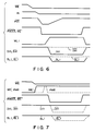
- a timing chart of Fig. 6 is obtained under conditions that an externally applied write enable signal WE is in an active state, i.e., in "0" level, and a logical state of input data IN changes from a "1" state to "0" state.
- the data transition detector 32 detects the transition and produces a detect signal ⁇ dt .
- this detect signal ⁇ dt is applied to the power down timer 34, the write power down timer 34 produces a pulse signal ⁇ wact , WE ⁇ each having a predetermined "L” duration.
- the energization of the word line is allowed by the gate circuit G1.
- the word line WL1 when the word line WL1 is selected, its potential rises as shown, and falls at the trailing edge of the pulse signal WE ⁇ .
- the pulse signal ⁇ wact , WE ⁇ is in "L"
- the write data corresponding to the input data IN is inputted to the write circuit 17, and the FETs Q3 and Q4 in the write circuit 17 are in an on state.
- the data lines Din and Din and the bit lines BL1 and BL1 are set at a potential based on the the input data.
- the write data is written into the memory cell MC1.
- the write operation is executed only during the "L" level period of the pulse signal ⁇ wact , WE ⁇ .
- the timing chart shown in Fig. 7 is depicted when the input data is "1" and the write enable signal WE changes from “H” to “L", viz., changes to an active state.
- the output signal WE′ of the NOR gate 41 rises to "H” level.
- the write mode detector 31 detects the signal WE′ of "H” level and produces a detect signal ⁇ we.
- the write power down timer 34 produces a pulse signal ⁇ wact , WE ⁇ each having a predetermined "L” duration.
- the word line WL1 is driven and the write data based on the input data is supplied to the write circuit 17.
- the input data IN is "1”
- the data lines Din and Din are respectively set at “H” and “L” levels, so that the bit lines BL1 and BL1 are also set at “H” and “L”, respectively.
- data "1” is written into the memory cell MC1.
- the pulse signal ⁇ wact , WE ⁇ goes high ("H") in level, the energization of the word line WL1 is inhibited. At the same time, the supply of the write data is prohibited. No data write operation will be performed.
- Fig. 8 shows a timing chart describing such a transient operation of the SRAM that the input data maintains a logical state "1", and the address signal continues a certain state, and under this condition, the write enable signal WE becomes active in a signal state, and then the address signal changes its contents.
- a detect signal ⁇ we derived from the write mode detector 31 causes the write power down timer 34 to produce a pulse signal ⁇ wact , WE ⁇ which is placed in "L" level during a predetermined period of time, as already stated.
- the word line corresponding to the input address for example, WL1
- the word line corresponding to the input address for example, WL1
- the paired data lines Din and Din are set in “H” and “L” level, respectively, and consequently the paired bit lines BL1 and BL1 are also set in in “H” and “L” level, respectively.
- This writing operation is executed only when the pulse signal ⁇ wact , WE ⁇ is in "L” level.
- the pulse signal ⁇ wact , WE ⁇ goes high ("H"), the word line is inhibited from being energized, while at the same time the supply of the write data is inhibited, and the writing operation stops.
- the address signal transition detector 33 In a state that the write enable signal WE is in an active state of "L" level, when the address signal changes, the address signal transition detector 33 produces a detect signal ⁇ at . In response to this signal, the write power down timer 34 produces a pulse signal ⁇ wact , WE ⁇ which is placed in "L” level during a predetermined period of time. Subsequently, the paired data lines Din and Din are set in “H” and “L” level, respectively, and then the paired bit lines BL1 and BL1 are also set in “H” and “L” level, respectively. Thereafter, when the address signal changes, a sequence of the operations like the above one is repeated.
- the provision of the address signal transition detector 33 enables control to access a plurality of memory cells of different addresses for write operation.
- the period of an actual write operation is limited by the pulse signal ⁇ wact , WE ⁇ . Accordingly, the power dissipation at the time of data writing operation is reduced.
- the period of executing an actual write operation can be uniquely determined within the SRAM circuit, not using an external control signal.
- the consume current of the SRAM according to the present invention is comparable with that of the conventional one with no power down function, when the writing operation is at a high speed more than 25 MHz. In a low speed write operation less than 25 MHz, the consume current is considerably reduced when comparing with that of the conventional SRAM.
- the control by the power down timer 34 is applied to the word line, and further the switch circuit (FETs Q3 and Q4) and the write buffers 101, 102 that are provided in the write circuit 17.
- the DC current saving may be realized by applying that control to the word line and the write buffers except the switch circuit (FETs Q3 and Q4). The reason for this is that when the output signals of the buffers 101 and 102 are in "H", no DC current flows even when the switch circuit (FETs Q3, Q4) is in an on state.
- the write power down timer 34 must produce a pulse signal WE ⁇ of a predetermined pulse width and a pulse signal ⁇ wact of a pulse width longer than that of the former. This is realized with substituting of two pulse width elongation circuits producing signals of different pulse widths for the pulse width elongation circuit 81 in Fig. 5. Of the pulse width signals, a shorter pulse width signal is coupled with the NOR gate 78 (Fig. 5) and a longer pulse width signal, with the NOR gate 75.
Landscapes
- Engineering & Computer Science (AREA)
- Microelectronics & Electronic Packaging (AREA)
- Theoretical Computer Science (AREA)
- Computer Hardware Design (AREA)
- Physics & Mathematics (AREA)
- General Engineering & Computer Science (AREA)
- General Physics & Mathematics (AREA)
- Static Random-Access Memory (AREA)
- Dram (AREA)
Claims (6)
- Statische Direktzugriffsspeichereinrichtung mit einer Speicherzellenanordnung, die eine Vielzahl von statischen Speicherzellen (MC1 bis MCn), ein Paar von Bitleitungen (BL1,
BL1 ) zum Transferieren von Daten nach und von den Speicherzellen in der Speicherzellenanordnung (BL1,BL1 ) und eine Schreibschaltung (17) zum Liefern von Schreibdaten an das Bitleitungspaar aufweist, wobei die statische Direktzugriffsspeichereinrichtung umfaßt:
Lasten (10) zum Laden der Bitleitungen;
eine Speicherzellen-Ansteuereinrichtung (13) zum selektiven Ansteuern einer der Speicherzellen über eine Ansteuer-Steuereinrichtung (G1) entsprechend einem Zeilenadressignal, welches von außen geliefert wird;
eine Schreibmodus-Erfassungseinrichtung (31) zum Erfassen eines Signalzustandsübergangs eines Schreibaktivierungssignals, welches sich auf einen aktiven Zustand ändert;
eine Eingangsdatenübergangserfassungseinrichtung (32) zur Erfassung eines Übergangs des von außen gelieferten Eingangsdatenwertes, während einer Fortdauer des aktiven Zustands des Schreibaktivierungssignals;
eine Adressignalübergangs-Erfassungseinrichtung (33) zur Erfassung eines Übergangs eines extern angelegten Adressignals während eines aktiven Zustands des Schreibaktivierungssignals;
eine Impulssignal-Erzeugungseinrichtung (34) zur Erzeugung eines Impulssignals mit einer vorgegebenen Impulsbreite im Ansprechen auf irgendeines der von der Schreibmodus-Erfassungseinrichtung (31), der Eingangsdatenübergangs-Erfassungseinrichtung (32) und der Adressignalübergangs-Erfassungseinrichtung (33) ausgegebenen Erfassungssignale;
wobei die Ansteuer-Steuereinrichtung (G1) der Speicherzellen-Ansteuereinrichtung (13) einen Betrieb während einer Periode erlaubt, in der die Impulssignal-Erzeugungseinrichtung (34) ein Impulssignal erzeugt und einen Betrieb der Speicherzellen-Ansteuereinrichtung (13) während einer Periode sperrt, in der die Impulssignal-Erzeugungseinrichtung ruht; und
eine Schreibschaltungs-Steuereinrichtung (35, 19) zum Liefern von Schreibdaten auf Grundlage der Eingangsdaten an die Schreibschaltung (17) während einer Periode, in der die Impulssignal-Erzeugungseinrichtung (34) ein Impulssignal erzeugt,
dadurch gekennzeichnet, daß
die Schreibsteuereinrichtung (35, 19) an die Schreibschaltungs-Anfangsdaten zum Setzen des Bitleitungspaars (BL1,BL1 ) auf die gleichen Potentiale während der Periode liefert, in der die Impulssignal-Erzeugungseinrichtung (34) ruht; und
die Impulssignal-Erzeugungseinrichtung (34) gleichzeitig ein erstes Impulssignal (WE˝ ) und ein zweites Impulssignal (Φwact ) einer breiteren Impulsbreite als die des ersten Impulssignals erzeugt, wobei das erste Impulssignal an die Ansteuer-Steuereinrichtung (G1) geliefert wird und das zweite Impulssignal an die Schreibschaltungs-Steuereinrichtung (35, 19) geliefert wird. - Statische Direktzugriffsspeichereinrichtung nach Anspruch 1,
dadurch gekennzeichnet, daß die
Schreibschaltung (17) Schreibpuffer (101, 102) zum Liefern von Schreibdaten an das Bitleitungspaar (BL1,BL1 ) und eine Umschaltschaltung (Q3, Q4), die zwischen die gepaarten Bitleitungen und die Schreibpuffer (101, 102) eingefügt ist, umfaßt, und die Umschaltschaltung (Q3, Q4) nur unter den Bedingungen eingeschaltet wird, daß das Schreibaktivierungssignal sich in einem aktiven Zustand befindet und die Impulserzeugungseinrichtung (34) ein Impulssignal erzeugt. - Statische Direktzugriffsspeichereinrichtung nach Anspruch 1,
dadurch gekennzeichnet, daß die
Speicherzellen-Ansteuereinrichtung (13) einen Zeilendekoder umfaßt. - Statische Direktzugriffsspeichereinrichtung nach Anspruch 3,
dadurch gekennzeichnet, daß die Ansteuer-Steuereinrichtung (G1) eine Gatterschaltung umfaßt, deren Gatterdurchschaltung durch das von der Impulssignal-Erzeugungseinrichtung (34) ausgegebene Impulssignal gesteuert wird, wobei die Gatterschaltung auf der Ausgangsseite des Zeilendekoders vorgesehen ist. - Statische Direktzugriffsspeichereinrichtung nach Anspruch 1,
dadurch gekennzeichnet, daß sie ferner eine Lastschaltung (10) umfaßt, die an einem Ende mit den gepaarten Bitleitungen (BL1,BL1 ) und an dem anderen Ende mit einem
Energiequellenpotentialversorgungsanschluß in einem ersten Logikpegel verbunden ist, und ferner dadurch gekennzeichnet, daß die Schreibschaltungs-Steuereinrichtung (35, 19) Schreibdaten auf Grundlage der Eingangsdaten an die Schreibschaltung (17) liefert, so daß während der Periode, in der die Impulssignal-Erzeugungseinrichtung (34) ein Impulssignal erzeugt, eine der gepaarten Bitleitungen (BL1,BL1 ) in den ersten Logikpegel eingestellt wird, während die andere in einen zweiten Logikpegel eingestellt wird, und daß die Schreibschaltungs-Steuereinrichtung (34, 19) an die Schreibschaltung (17) Schreibdaten liefert, um beide gepaarten Bitleitungen (BL1,BL1 ) in den ersten Logikpegel während der Periode einzustellen, in der die Impulssignal-Erzeugungseinrichtung (34) ruht. - Statische Direktzugriffsspeichereinrichtung nach Anspruch 1,
dadurch gekennzeichnet, daß die Schreibschaltung (17) Schreibpuffer (101, 102) zum Liefern von Schreibdaten an das Bitleitungspaar (BL1,BL1 ) und eine Umschaltschaltung (Q3, Q4) umfaßt, die zwischen die gepaarten Bitleitungen und die Schreibpuffer (101, 102) eingefügt ist;
wobei die Umschaltschaltung (Q3, Q4) angeordnet ist, so daß sie nur unter den Bedingungen eingeschaltet wird, daß sich das Schreibaktivierungssignal in einem aktiven Zustand befindet und die Impulserzeugungseinrichtung (34) ein Impulssignal erzeugt; und
die Umschaltschaltung (Q3, Q4) angeordnet ist, um die Bitleitungen von den Schreibpuffern (101, 102) zu trennen, wenn die Umschaltschaltung (Q3, Q4) ausgeschaltet wird.
Applications Claiming Priority (2)
| Application Number | Priority Date | Filing Date | Title |
|---|---|---|---|
| JP63078785A JPH01251496A (ja) | 1988-03-31 | 1988-03-31 | スタティック型ランダムアクセスメモリ |
| JP78785/88 | 1988-03-31 |
Publications (3)
| Publication Number | Publication Date |
|---|---|
| EP0347530A2 EP0347530A2 (de) | 1989-12-27 |
| EP0347530A3 EP0347530A3 (de) | 1991-04-03 |
| EP0347530B1 true EP0347530B1 (de) | 1995-05-24 |
Family
ID=13671538
Family Applications (1)
| Application Number | Title | Priority Date | Filing Date |
|---|---|---|---|
| EP89105247A Expired - Lifetime EP0347530B1 (de) | 1988-03-31 | 1989-03-23 | Statische RAM-Speicheranordnung mit einer Leistungsverminderungsfunktion |
Country Status (5)
| Country | Link |
|---|---|
| US (1) | US4962487A (de) |
| EP (1) | EP0347530B1 (de) |
| JP (1) | JPH01251496A (de) |
| KR (1) | KR930011786B1 (de) |
| DE (1) | DE68922787T2 (de) |
Families Citing this family (28)
| Publication number | Priority date | Publication date | Assignee | Title |
|---|---|---|---|---|
| US5228003A (en) * | 1988-04-15 | 1993-07-13 | Seiko Epson Corporation | Semiconductor memory |
| US5287525A (en) * | 1989-11-29 | 1994-02-15 | Linear Technology Corporation | Software controlled power shutdown in an integrated circuit |
| JP2740063B2 (ja) * | 1990-10-15 | 1998-04-15 | 株式会社東芝 | 半導体記憶装置 |
| US5124584A (en) * | 1990-10-22 | 1992-06-23 | Sgs-Thomson Microelectronics, Inc. | Address buffer circuit with transition-based latching |
| US5215615A (en) * | 1990-12-21 | 1993-06-01 | E. I. Du Pont De Nemours And Company | Process for multiple yarn winding in ordered fashion and resulting product |
| JP2876830B2 (ja) * | 1991-06-27 | 1999-03-31 | 日本電気株式会社 | 半導体記憶装置 |
| JPH0520877A (ja) * | 1991-07-16 | 1993-01-29 | Mitsubishi Electric Corp | 半導体記憶装置 |
| JP2868650B2 (ja) * | 1991-07-24 | 1999-03-10 | キヤノン株式会社 | 表示装置 |
| JP3587542B2 (ja) * | 1992-06-19 | 2004-11-10 | インテル・コーポレーション | 電力消費を節減する方法および装置 |
| JP2838967B2 (ja) * | 1993-12-17 | 1998-12-16 | 日本電気株式会社 | 同期型半導体装置用パワーカット回路 |
| KR0141933B1 (ko) * | 1994-10-20 | 1998-07-15 | 문정환 | 저전력의 스테이틱 랜덤 억세스 메모리장치 |
| JP3290315B2 (ja) * | 1994-11-15 | 2002-06-10 | 三菱電機株式会社 | 半導体記憶装置 |
| US5633828A (en) * | 1995-08-24 | 1997-05-27 | Sgs-Thomson Microelectronics, Inc. | Circuitry and methodology to test single bit failures of integrated circuit memory devices |
| US5636177A (en) * | 1996-01-16 | 1997-06-03 | United Microelectronics Corp. | Static random access memory with improved noise immunity |
| US5864696A (en) * | 1996-01-19 | 1999-01-26 | Stmicroelectronics, Inc. | Circuit and method for setting the time duration of a write to a memory cell |
| JPH09282886A (ja) * | 1996-01-19 | 1997-10-31 | Sgs Thomson Microelectron Inc | メモリセルへの書込の開始をトラッキングする回路及び方法 |
| JPH09231770A (ja) * | 1996-01-19 | 1997-09-05 | Sgs Thomson Microelectron Inc | メモリセルへの書込を終了させる回路及び方法 |
| JPH1063581A (ja) * | 1996-08-26 | 1998-03-06 | Nec Corp | メモリ書き込み制御回路 |
| US5949261A (en) | 1996-12-17 | 1999-09-07 | Cypress Semiconductor Corp. | Method and circuit for reducing power and/or current consumption |
| US5764592A (en) * | 1996-12-21 | 1998-06-09 | Sgs-Thomson Microelectronics, Inc. | External write pulse control method and structure |
| US5864509A (en) * | 1997-02-21 | 1999-01-26 | Cypress Semiconductor Corp. | Method and apparatus for reducing continuous write cycle current in memory device |
| KR100253282B1 (ko) * | 1997-04-01 | 2000-05-01 | 김영환 | 메모리소자의소모전력자동감소회로 |
| US6181640B1 (en) | 1997-06-24 | 2001-01-30 | Hyundai Electronics Industries Co., Ltd. | Control circuit for semiconductor memory device |
| US6741111B1 (en) | 2003-04-21 | 2004-05-25 | Pericom Semiconductor Corp. | Data register for buffering double-data-rate DRAMs with reduced data-input-path power consumption |
| US8264862B2 (en) | 2010-11-24 | 2012-09-11 | Lsi Corporation | Low power SRAM based content addressable memory |
| US11100962B2 (en) * | 2017-12-26 | 2021-08-24 | SK Hynix Inc. | Semiconductor device with a power-down mode and a power gating circuit and semiconductor system including the same |
| US11838020B1 (en) | 2017-12-26 | 2023-12-05 | SK Hynix Inc. | Semiconductor memory device including write driver with power gating structures and operating method thereof |
| US10943626B1 (en) | 2017-12-26 | 2021-03-09 | SK Hynix Inc. | Semiconductor memory device with power gating circuit for data input-output control block and data input/output block and semiconductor system including the same |
Family Cites Families (14)
| Publication number | Priority date | Publication date | Assignee | Title |
|---|---|---|---|---|
| JPS54136239A (en) * | 1978-04-14 | 1979-10-23 | Nec Corp | Integrated circuit |
| US4337525A (en) * | 1979-04-17 | 1982-06-29 | Nippon Electric Co., Ltd. | Asynchronous circuit responsive to changes in logic level |
| JPS56137580A (en) * | 1980-03-26 | 1981-10-27 | Nec Corp | Semiconductor storage device |
| JPS58147883A (ja) * | 1982-02-26 | 1983-09-02 | Toshiba Corp | スタテイツク型ブ−トストラツプ回路を備えた半導体集積回路 |
| JPS5956292A (ja) * | 1982-09-24 | 1984-03-31 | Hitachi Ltd | 半導体記憶装置 |
| JPS5975486A (ja) * | 1982-10-22 | 1984-04-28 | Hitachi Ltd | Mosスタテイツク型ram |
| JPS59221891A (ja) * | 1983-05-31 | 1984-12-13 | Toshiba Corp | スタテイツク型半導体記憶装置 |
| JPS6124091A (ja) * | 1984-07-12 | 1986-02-01 | Nec Corp | メモリ回路 |
| US4636991A (en) * | 1985-08-16 | 1987-01-13 | Motorola, Inc. | Summation of address transition signals |
| JPH0612626B2 (ja) * | 1986-01-22 | 1994-02-16 | 株式会社日立製作所 | 半導体メモリ装置 |
| JPS62254460A (ja) * | 1986-04-26 | 1987-11-06 | Toshiba Corp | Bi−CMOS論理回路 |
| JPH0831275B2 (ja) * | 1986-09-09 | 1996-03-27 | 日本電気株式会社 | メモリ回路 |
| JPS6383991A (ja) * | 1986-09-29 | 1988-04-14 | Toshiba Corp | スタテイツク型メモリ |
| JPS63166090A (ja) * | 1986-12-26 | 1988-07-09 | Toshiba Corp | スタティック型メモリ |
-
1988
- 1988-03-31 JP JP63078785A patent/JPH01251496A/ja active Pending
-
1989
- 1989-03-23 DE DE68922787T patent/DE68922787T2/de not_active Expired - Fee Related
- 1989-03-23 EP EP89105247A patent/EP0347530B1/de not_active Expired - Lifetime
- 1989-03-30 KR KR8904080A patent/KR930011786B1/ko not_active Expired - Fee Related
-
1990
- 1990-02-21 US US07/483,988 patent/US4962487A/en not_active Expired - Lifetime
Non-Patent Citations (1)
| Title |
|---|
| 747, New York, US; W.C.H. GUBBELS et al.: "A 40-ns/ 100-pF low-power full-CMOS256K (32K X 8) SRAM" * |
Also Published As
| Publication number | Publication date |
|---|---|
| DE68922787T2 (de) | 1995-11-16 |
| JPH01251496A (ja) | 1989-10-06 |
| KR930011786B1 (en) | 1993-12-21 |
| EP0347530A2 (de) | 1989-12-27 |
| US4962487A (en) | 1990-10-09 |
| EP0347530A3 (de) | 1991-04-03 |
| DE68922787D1 (de) | 1995-06-29 |
| KR890015271A (ko) | 1989-10-28 |
Similar Documents
| Publication | Publication Date | Title |
|---|---|---|
| EP0347530B1 (de) | Statische RAM-Speicheranordnung mit einer Leistungsverminderungsfunktion | |
| US5426755A (en) | Semiconductor device including clock selection circuitry selecting between high and low frequency clock signals for reduced power consumption | |
| US7123541B2 (en) | Memory with address management | |
| EP0649146B1 (de) | Integrierte Halbleiterschaltungsanordnung | |
| EP0186906B1 (de) | Halbleiterspeicher mit einer hohen Datenlesegeschwindigkeit und einem hohen Störabstand | |
| EP0533096B1 (de) | Adressiersystem ohne Vielfach-Selektion der Word-Leitungen | |
| US5969995A (en) | Static semiconductor memory device having active mode and sleep mode | |
| US6031781A (en) | Semiconductor memory device allowing high-speed activation of internal circuit | |
| US5357479A (en) | Static random access memory capable of preventing erroneous writing | |
| US4618784A (en) | High-performance, high-density CMOS decoder/driver circuit | |
| US4987560A (en) | Semiconductor memory device | |
| US5400285A (en) | Semiconductor integrated circuit device | |
| EP0259862B1 (de) | Halbleiterspeicher mit Schreibfunktion | |
| US4933905A (en) | Semiconductor memory device for reducing power dissipation during a write operation | |
| EP0337172B1 (de) | Statische RAM-Speicheranordnung mit einer Leistungsverminderungsfunktion | |
| US5384730A (en) | Coincident activation of pass transistors in a random access memory | |
| EP0646926B1 (de) | Schaltung zum Abschalten eines Flankendetektors zum Ändern der Betriebscharakteristiken eines Speichers | |
| US5461593A (en) | Word-line driver for a semiconductor memory device | |
| US6061286A (en) | Memory device with reduced power dissipation | |
| US4610003A (en) | Dynamic type semiconductor memory device | |
| EP0228958B1 (de) | Halbleiterspeicheranordnung mit einer Rücksetzsignalgeneratorschaltung | |
| US7032083B1 (en) | Glitch-free memory address decoding circuits and methods and memory subsystems using the same | |
| US4825410A (en) | Sense amplifier control circuit | |
| US6473347B2 (en) | Semiconductor device having memory with effective precharging scheme | |
| JPS60119691A (ja) | メモリ回路 |
Legal Events
| Date | Code | Title | Description |
|---|---|---|---|
| PUAI | Public reference made under article 153(3) epc to a published international application that has entered the european phase |
Free format text: ORIGINAL CODE: 0009012 |
|
| 17P | Request for examination filed |
Effective date: 19890323 |
|
| AK | Designated contracting states |
Kind code of ref document: A2 Designated state(s): DE FR GB |
|
| PUAL | Search report despatched |
Free format text: ORIGINAL CODE: 0009013 |
|
| AK | Designated contracting states |
Kind code of ref document: A3 Designated state(s): DE FR GB |
|
| 17Q | First examination report despatched |
Effective date: 19921218 |
|
| GRAA | (expected) grant |
Free format text: ORIGINAL CODE: 0009210 |
|
| AK | Designated contracting states |
Kind code of ref document: B1 Designated state(s): DE FR GB |
|
| REF | Corresponds to: |
Ref document number: 68922787 Country of ref document: DE Date of ref document: 19950629 |
|
| ET | Fr: translation filed | ||
| PLBE | No opposition filed within time limit |
Free format text: ORIGINAL CODE: 0009261 |
|
| STAA | Information on the status of an ep patent application or granted ep patent |
Free format text: STATUS: NO OPPOSITION FILED WITHIN TIME LIMIT |
|
| 26N | No opposition filed | ||
| PGFP | Annual fee paid to national office [announced via postgrant information from national office to epo] |
Ref country code: GB Payment date: 19970314 Year of fee payment: 9 |
|
| PGFP | Annual fee paid to national office [announced via postgrant information from national office to epo] |
Ref country code: DE Payment date: 19970401 Year of fee payment: 9 |
|
| PG25 | Lapsed in a contracting state [announced via postgrant information from national office to epo] |
Ref country code: GB Free format text: LAPSE BECAUSE OF NON-PAYMENT OF DUE FEES Effective date: 19980323 |
|
| GBPC | Gb: european patent ceased through non-payment of renewal fee |
Effective date: 19980323 |
|
| PG25 | Lapsed in a contracting state [announced via postgrant information from national office to epo] |
Ref country code: DE Free format text: LAPSE BECAUSE OF NON-PAYMENT OF DUE FEES Effective date: 19981201 |
|
| REG | Reference to a national code |
Ref country code: FR Ref legal event code: D6 |
|
| PGFP | Annual fee paid to national office [announced via postgrant information from national office to epo] |
Ref country code: FR Payment date: 20070308 Year of fee payment: 19 |
|
| REG | Reference to a national code |
Ref country code: FR Ref legal event code: ST Effective date: 20081125 |
|
| PG25 | Lapsed in a contracting state [announced via postgrant information from national office to epo] |
Ref country code: FR Free format text: LAPSE BECAUSE OF NON-PAYMENT OF DUE FEES Effective date: 20080331 |