EP0345757A2 - Veraschungsverfahren zum Entfernen einer organischen Schicht auf einer Halbleiteranordnung während ihrer Herstellung - Google Patents
Veraschungsverfahren zum Entfernen einer organischen Schicht auf einer Halbleiteranordnung während ihrer Herstellung Download PDFInfo
- Publication number
- EP0345757A2 EP0345757A2 EP89110295A EP89110295A EP0345757A2 EP 0345757 A2 EP0345757 A2 EP 0345757A2 EP 89110295 A EP89110295 A EP 89110295A EP 89110295 A EP89110295 A EP 89110295A EP 0345757 A2 EP0345757 A2 EP 0345757A2
- Authority
- EP
- European Patent Office
- Prior art keywords
- gas
- ashing
- oxygen
- reactant gas
- plasma
- Prior art date
- Legal status (The legal status is an assumption and is not a legal conclusion. Google has not performed a legal analysis and makes no representation as to the accuracy of the status listed.)
- Granted
Links
Images


Classifications
-
- H—ELECTRICITY
- H01—ELECTRIC ELEMENTS
- H01L—SEMICONDUCTOR DEVICES NOT COVERED BY CLASS H10
- H01L21/00—Processes or apparatus adapted for the manufacture or treatment of semiconductor or solid state devices or of parts thereof
- H01L21/02—Manufacture or treatment of semiconductor devices or of parts thereof
- H01L21/04—Manufacture or treatment of semiconductor devices or of parts thereof the devices having at least one potential-jump barrier or surface barrier, e.g. PN junction, depletion layer or carrier concentration layer
- H01L21/18—Manufacture or treatment of semiconductor devices or of parts thereof the devices having at least one potential-jump barrier or surface barrier, e.g. PN junction, depletion layer or carrier concentration layer the devices having semiconductor bodies comprising elements of Group IV of the Periodic System or AIIIBV compounds with or without impurities, e.g. doping materials
- H01L21/30—Treatment of semiconductor bodies using processes or apparatus not provided for in groups H01L21/20 - H01L21/26
- H01L21/31—Treatment of semiconductor bodies using processes or apparatus not provided for in groups H01L21/20 - H01L21/26 to form insulating layers thereon, e.g. for masking or by using photolithographic techniques; After treatment of these layers; Selection of materials for these layers
- H01L21/3105—After-treatment
- H01L21/311—Etching the insulating layers by chemical or physical means
- H01L21/31127—Etching organic layers
- H01L21/31133—Etching organic layers by chemical means
- H01L21/31138—Etching organic layers by chemical means by dry-etching
-
- G—PHYSICS
- G03—PHOTOGRAPHY; CINEMATOGRAPHY; ANALOGOUS TECHNIQUES USING WAVES OTHER THAN OPTICAL WAVES; ELECTROGRAPHY; HOLOGRAPHY
- G03F—PHOTOMECHANICAL PRODUCTION OF TEXTURED OR PATTERNED SURFACES, e.g. FOR PRINTING, FOR PROCESSING OF SEMICONDUCTOR DEVICES; MATERIALS THEREFOR; ORIGINALS THEREFOR; APPARATUS SPECIALLY ADAPTED THEREFOR
- G03F7/00—Photomechanical, e.g. photolithographic, production of textured or patterned surfaces, e.g. printing surfaces; Materials therefor, e.g. comprising photoresists; Apparatus specially adapted therefor
- G03F7/26—Processing photosensitive materials; Apparatus therefor
- G03F7/42—Stripping or agents therefor
- G03F7/427—Stripping or agents therefor using plasma means only
Definitions
- the present invention relates to a removing method of an organic material used in a semiconductor device, and particularly the present invention relates to an ashing method of an organic film temporarily formed on a substance of a semiconductor device under fabrication.
- An organic film such as a resist or a polyimide film temporarily formed on a substance, which is a part of a semiconductor device, for fabricating the semiconductor device was usually removed by an ashing method using oxygen plasma. Removing the resist film is an important process in fabrication of the semiconductor device, removing the resist film as an organic film will be described, hereinafter. Since the semiconductor device becomes very small as a Large Scale Integration circuit device (LSI) or a Very Large Scale Integrated circuit device (VLSI), the resist film, which will be called simply the "resist” hereinafter, becomes hard to be removed by the usual ashing method using the oxygen plasma without damaging the devices.
- LSI Large Scale Integration circuit device
- VLSI Very Large Scale Integrated circuit device
- the property of the resist is changed during the process of ion implantation and dry etching, which are widely performed in the fabricating process of the LSI or the VLSI, so that a long time is required for performing ashing, in other words, the ashing rate of the resist becomes small. Since the resist is used many times in the fabrication process of the LSI or the VLSI, the ashing rate for each resist should be large to improve the throughput of the fabrication of the LSI or the VLSI.
- a layer, called simply a "ground layer” hereinafter and the resist is formed thereon, is usually made of material such as silicon dioxide (SiO2), polysilicon (Si) or aluminum (Al).
- the resist is not easy to be etched intentionally by the the ashing method, in other words, the resist is hard to be etched precisely so as to be removed only the resist without damaging any of the ground layer in the ashing process. Therefore, when the ashing method is applied to the fabricating process of the LSI or the VLSI, great attention must be paid to leave the ground layer as it is. Because, the ground layer of the LSI or the VLSI is very thin and any little part of it is not allowed to be etched.
- the down stream ashing rate generally depends on a temperature, which will be called an "ashing temperature" hereinafter, of the resist so that the ashing rate decreases with the decrease of the ashing temperature.
- the ashing rate is usually expressed by the well known Arrhenius plot by which the ashing rates are plotted in a line against the inverse numbers of the respective ashing temperatures.
- the gradient of the line gives the activation energy for ashing in such that when the ashing rate decreases rapidly with the decrease of the ashing temperature, the activation energy is large, and when the ashing rate changes only little with the decrease of the ashing temperature, the activation energy is small.
- the small activation energy is desirable because the ashing can be performed almost independently on the ashing temperature, in other words, the ashing can be performed in stable and precisely.
- a wafer process in the fabrication process of a semiconductor device is performed at a lower temperature according as the semiconductor device has a higher integration circuit as seen in the LSI or the VLSI.
- the ashing process is desired to be performed lower than 300°C, most preferably lower than 200°C to avoid contamination from the resist.
- the activation energy of the ashing rate must be also small.
- the activation energy of the ashing rate can be changed to some extent by changing the species of reactant gases used for ashing.
- the selection and the combination of the reactant gases are very important for making the ashing rate high and the activation energy small and for etching the resist precisely, leaving the ground layer as perfectly as possible and for minimizing damage.
- the selection and the combination of the reactant gases has been studied energetically.
- the downstream ashing is performed in a downstream of a microwave plasma using a microwave plasma resist stripper. This is fully disclosed in the paper titled "Heavy Metal Contamination From Resists during Plasma Stripping" by Shuzo Fujimura and Hiroshi Yano, in Elect. Chem. Soc. Vol. 135, No. 5, May 1988. .
- the downstream of a microwave plasma resist stripper consists of a vacuum chamber including a plasma generating chamber, a vacuum pump for exhausting gas in the vacuum chamber, a process chamber including a pedestal on which a sample wafer is placed and a microwave power source.
- a reactant gas is supplied to the process chamber through the plasma generating chamber.
- a reactant gas plasma is generated in the plasma generating chamber by the microwaves, so that active species for ashing produced in the gas plasma flows down to the process chamber and reacts with a resist previously formed on the sample wafer so as to remove the resist.
- a first reactant gas was a mixed gas of oxygen (O2) with a halogenide gas such as tetrafluoromethane (CF4).
- the first reactant gas was most commonly used because it had a large ashing rate.
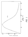
- Fig. 1 shows the ashing rate for commercially available photoresist(OFPR-800, TOKYO-OHKA) plotted against the variation of flow ratio of tetrafluoromethane to the mixed gas at room temperature.
- the ashing rate in the case using a reactant gas is simply called the ashing rate with the reactant gas, hereinafter.
- a second reactant gas was a mixed gas of oxygen and nitrogen (N2), not containing fluorine (F), which did not etch the ground layer.
- the ashing rate and the concentration of oxygen atom in a down-flowed gas were measured by varying the flow ratio of nitrogen to the second reactant gas as shown in Fig. 2; wherein, the concentration of oxygen atom was measured by an actinometry method.
- the ashing temperature was 200°C and the flow rate of the second reactant gas was 1000 Standard Cubic Centimeter per Minute (SCCM).
- SCCM Standard Cubic Centimeter per Minute
- white circles represent the concentrations of oxygen atom, obtained from the spectral intensity ratio of the radiation from an oxygen atom (at a wavelength of 6158 ⁇ ) to the radiation from an argon atom (at a wavelength of 7067 ⁇ ) and triangles represent the concentrations of the same oxygen atom, obtained from the spectral intensity ratio of the radiation from an oxygen atom (at a wave length of 4368 ⁇ ) to the radiation from an argon atom (at a wavelength of 7067 ⁇ ).
- the values of these concentrations are normalized by a maximum of the values of the concentrations, positioned at about 10% of the flow ratio of nitrogen to the second reactant gas. Multiplication signs represent the ashing rates to the flow ratio of nitrogen to the second reactant gas.
- Fig. 2 shows the curve of the ashing rate and that of the concentration of oxygen atom which means that oxygen atoms are only effective in performing the ashing.
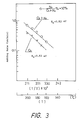
- Fig. 3 shows the Arrhenius plot of the ashing rate when the second reactant gas contains 90% of oxygen and 10% of nitrogen in the flow ratio and the Arrhenius plot of the oxygen gas only.
- the ashing temperature is denoted by T.
- the ashing rate of the second reactant gas is plotted by a circle and the ashing rate of the oxygen is plotted by a multiplication sign.
- the ashing rate with the second reactant gas is about two times of that of oxygen only.
- the activation energy of ashing in the case using a reactant gas is simply called the activation energy of the reactant gas, hereinafter.
- the activation energy (Ea) of the second reactive gas, and that of the oxygen are equally 0.52 eV. That is, the activation energy does not change by mixing nitrogen.
- the ashing rate of the second reactive gas of 0.2 ⁇ m/min at 160 °C is too small for practical use. In order to increase the ashing rate, another kind of gas was needed.
- the third reactant gas was a mixed gas of oxygen and water vapor (H2O) which did not etch the ground layer.
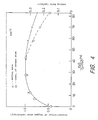
- the ashing rate and concentration of oxygen atom were measured by varying the flow ratios of water vapor to the third reactant gas as shown in Fig. 4. The measurements were performed under 180°C ashing temperature and 1000 SCCM flow rate of the third reactant gas. Circles and multiplication signs in Fig. 4 represent the same as in Fig. 2 respectively.
- the flow ratio of water vapor to the third reactant gas exceeds 40%, the concentration of the oxygen atom decreases with the increase of the water vapor flow ratio. However, the ashing rate does not decrease so much as the decrease of the concentration of oxygen atom as seen in Fig. 4.
- Fig. 5 compares the Arrhenius plot of the third reactant gas containing 60% of oxygen and 40% of water vapor and Arrhenius plot of the oxygen gas.
- the ashing rate of the third reactant gas having 40% flow ratio of water vapor is plotted by triangles and the ashing rate of the oxygen is plotted by multiplication signs.
- the activation energy of the third reactive gas is 0.39 eV which is about three quarter of the activation energy (0.52 eV) of oxygen as shown in Fig. 6.
- Fig. 6 shows the activation energy of the ashing in the case using the third reactant gas by varying the flow ratios of water vapor to the third reactant gas, by white circles.
- Fig. 6 the activation energy of ashing in the case using the mixed gas of oxygen and hydrogen by varying the flow ratio of hydrogen to the mixed gas is shown by solid circles, for the sake of comparison. It is seen in Fig. 6 that the activation energy is easily reduced by adding water vapor a little and the activation energy is constant independently on the flow ratio of water vapor when the flow ratio of water vapor exceeds 5%.
- the activation energy of the second reactant gas is also indicated by a dot chain line in Fig. 6 for the comparison with the third reactant gas. It is seen from this comparison that the activation energy does not change by adding nitrogen to oxygen. The behavior similar to the mixed gas of oxygen and water vapor is seen for the mixed gas of oxygen and hydrogen.
- the ashing rate of the third reactant gas is about o.22 ⁇ m/min at 160°C, as seen in Fig. 5.
- the value of the ashing rate of the third reactant gas is still too small for practical use.
- the fourth reactant gas is a mixed gas of oxygen, nitrogen and tetrafluoromethane.
- the fourth reactant gas is disclosed in the Japanese laid-open patent application, SHO 63-102232, titled “DRY ETCHING APPARATUS" by Mikio Nonaka.
- the flow ratio of tetrafluoromethane and nitrogen are in the range of 5 to 20% and 5 to 10% respectively, the large ratio of a rate of etching a positive resist to a rate of etching a ground layer is obtained without decreasing the ashing rate.
- the etching of ground layer can not be avoided occurring in this case.
- a mixed gas made by adding as little as 0.2% of hydrogen to a mixed gas of oxygen, nitrogen and tetrafluoromethane is commercially available from EMERGENT TECHNOLGIES CO.(Phoenix 2320 NORD Photoresist Stripper).
- the hydrogen diluted by nitrogen is added in order to improve matching with microwave power. That is, the adding hydrogen to the mixed gas is not for reduction of the activation energy. So, the mixed gas is essentially the same as the first reactant gas. In fact, it is also known that the activation energy of the second reactant gas mixed with hydrogen does not decrease until up to 0.5% of hydrogen.
- an object of the present invention is to improve the ashing process for removing the organic film formed on the ground layer of the semiconductor device under fabrication, so that the ashing rate increases, the activation energy decreases and the ground layer is never etched in the ashing process.
- the above object is achieved by applying a reactant gas composed of at least three kinds of gases to the ashing process.
- the reactant gas is separated into two group mixed gases one (a first group gas) of which is composed of at least oxygen and water vapor and the other (a second group gas) of which is composed of at least oxygen and hydrogen.
- oxygen in each group gas is a main gas for performing the ashing, however water vapor in the first group gas and hydrogen in the second group gas are for mainly decreasing the activation energy, increasing the ashing rate and avoiding the ground layer being etched in cooperation with another third gas respectively added to the first group gas and the second group gas.
- the third gas added to the first group gas is hydrogen, nitrogen, nitrogen oxide or halogenide and that added to the second group gas is water vapor, nitrogen, nitrogen oxide or halogenide.
- the halogenide includes tetrafluoromethane(CF4), chlorine(Cl2), nitrogen trifluoride(NF3), hexafluoroethane(C2F6) and trifluoromethane(CHF3).
- the water vapor added to oxygen has the same effect of that described in reference to Fig. 5, and the added nitrogen has the same effect of that described in reference to Fig. 3.
- these added water vapor and nitrogen produce a synergetic effect on increasing the ashing rate and decreasing the activation energy. That is, it was simply assumed from Figs. 3 and 5 that the ashing rate of the first group gas including the third gas of nitrogen would increase in the same way as the case of a gas only mixing oxygen and nitrogen and the activation energy of the first group gas including the third gas of nitrogen would decrease in the same way as the case of a gas only mixing oxygen and water vapor. However, actually, the ashing rate increases as much as two times of the assumed value from Fig. 3 though the activation energy decreases to a value approximately same of the value assumed from Fig. 5.
- the first group gas including the third gas of halogenide such as tetrafluoromethane is excellent as the reactant gas.
- halogenide has not been used as the third gas in the fabrication of the LSI or the VLSI because of disadvantage that halogen easily etches the ground layer.
- the first group gas including the third gas of halogenide does not etch the ground layer when the water vapor is included in the reactant gas, supplied by a flow ratio controlled so as to exceed a designated value. Because, the halogen atoms react to the hydrogen atoms of the water molecules. As the result, the action of the halogen is suppressed.
- the first group gas including the third gas of halogen as the reactant gas, the ashing rate becomes large and the activation energy of the ashing rate becomes small, compared with the first group gas including the third gas of nitrogen.
- the activation energy is decreased to 0.44 eV from 0.52 eV by adding hydrogen of more than 3%; wherein 0.52 eV is the activation energy corresponding to the oxygen. This is because of that the hydrogen acts to decrease the activation energy.
- the ashing rate of the second group gas including the third gas of nitrogen is large as much as two or three times of that of the usual mixed gas of oxygen and nitrogen.
- These mixed gases, described above, of the first group gas including nitrogen as the third gas, the first group gas including hologenide as the third gas and the second group gas have three advantages of having a large ashing rate, having small activation energy and etching no ground layer in the fabrication process of the LSI or the VLSI.
- the plasma ashing methods of removing the resist, using three kinds of reactant gases will be described as the embodiments of the present invention, in reference to Figs. 8 to 12.
- the embodiments are separated into three, a first, a second and a third embodiment, in accordance with the three kinds of the reactant gases.
- the plasma ashing are performed by a down flow ashing method using a conventional downstream microwave plasma resist stripper schematically shown in Fig. 7.
- the first embodiment is the plasma ashing method using a reactant gas composed of O2, H2O and N2.
- the reactant gas composed of 720 SCCM O2, 100 SCCM H2O and 180 SCCM N2 is supplied to an initially exhausted vacuum chamber 6 through a gas inlet 3, keeping the gas pressure in the vacuum chamber 6 at about 0.8 Torr.
- the flow rates of the gases of O2, H2O and N2 are controlled respectively by a controller, not depicted, before the gases flow into the vacuum chamber 6.
- microwave power of 2.45 GHz is supplied into a plasma generating chamber 4. Plasma is generated with the reactant gas in the plasma generating chamber 4 and the charged particles in the plasma are trapped by a shower plate 5.
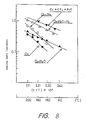
- the ashing rate in the case of using the reactant gas composed of O2, H2O and N2 is shown by a line connecting white triangles in Fig. 8 represented in Arrhenius plot.
- the ashing rates in the case of using other several kinds of reactant gases are also shown in the same way, for the sake of comparison. That is, the ashing rate in the case of using the reactant gas composed of only O2, that of using the reactant gas composed of O2 and H2O and that of using the reactant gas composed of O2 and N2 are shown by solid circle, solid triangle and white circle respectively. As seen in Fig.
- the ashing rate in the case of using the reactant gas of O2, H2O and N2 is larger than the ashing rate in the cases of using the reactant gas composed of only O2, of O2 and H2O, and of O2 and N2.
- the reactant gas composed of O2, H2O and N2 has the ashing rate of 0.5 ⁇ m/min at 160°C ashing temperature and the activation energy of 0.4 eV.
- the 0.5 ⁇ m/min ashing rate is large enough and the 0.4 eV activation energy is small enough.
- FIG. 9 shows the variation of the ashing rate for the various flow ratios of N2 to the mixed gas of O2 and N2, at the ashing temperature of 180°C and that of 200°C, keeping the flow rate of H2O in 100 SCCM and the total flow rate of O2 and N2 in 900 SCCM. It can be seen in Fig. 9 that the ashing rate in the case of using the reactant gas composed of O2, H2O and N2 is hardly changed by varying the flow ratio of nitrogen to the mixed gas of O2 and N2 when the flow ratio is larger than 5%. Therefore, the reactant gas of mixing O2, H2O and N2 having the flow ratio larger than 5% can be also used as the reactant gas for performing a precise ashing process.
- the flow rate of each component gas is set 720 SCCM, 100 SCCM and 180 SCCM for O2, H2O and N2, respectively, as a desirable example.
- flow rate of N2 is not limited if the flow ratio of N2 to the mixed gas of O2 and N2 is larger than 5%, because the ashing rate is constant regardless of the flow ratio when the flow ratio exceeds 5% as seen in Fig. 9.
- the flow rate of H2O is not limited if the flow ratio of H2O to the mixed gas of O2 and H2O is larger than 1%, because the activation energy is about 0.4 eV regardless of the flow ratio when the flow ratio exceeds 1%, as seen in Fig. 6.
- NO x or H2 can be added to the mixed gas of O2 and H2O instead of N2.
- the reactant gas composed of O2, H2O and CF4 is used for the plasma ashing.
- the ashing is performed in the same way as described in the first embodiment.
- the flow rates of O2, H2O and CF4 are 730 SCCM, 150 SCCM and 120 SCCM, respectively.
- Fig. 10 is a graph showing the etching rate, at 150°C and 25°C ashing temperature, of a ground layer made of SiO2, with the flow ratio of H2O to the reactant gas, under a condition that the total flow rate of O2, H2O and CF4 is kept in 1000 SCCM and the flow ratio of CF4 to the mixed gas of O2 + CF4 is kept in 15%. From Fig.
- the ashing rate of the reactant gas composed of O2, H2O and CF4 is shown by a line connecting reversed solid triangles in Fig. 8. As shown in Fig. 8, the ashing rate is the largest, compared with other ashing rates in the cases of using other reactant gases.
- the ashing rate of the reactant gas composed of O2, H2O and CF4 was measured by varying the flow ratio of H2O to the reactant gas at 25°C, 150°C and 180°C ashing temperature respectively, under a condition that the total flow rate of O2, H2O and CF4 was kept in 1000 SCCM and the flow ratio of CF4 to the mixed gas of O2 and CF4 was kept in 15% .
- the results of the measurement are shown in Fig. 11 where it can be seen that when the flow ratio of H2O to the reactant gas exceeds 10%, the ashing rate is constant and independent of flow ratio of H2O to the reactant gas.
- the flow rate of each component gas is set 730 SCCM, 150 SCCM and 120 SCCM for O2, H2O and CF4, respectively, as a desirable example.
- flow rate of H2O is not limited if the number of hydrogen atoms of H2O is larger than the number of fluorine atoms liberated from CF4.
- the flow ratio of H2O to the mixed gas of O2 and H2O must be larger than 1%, so that the activation energy of ashing in the case of using the reactant gas is about 0.4 eV regardless of the flow ratio, as seen in Fig. 6.
- CF4 is used as a halogenide, however Cl2, NF3, C2F6 and CHF3 can be used instead of CF4.
- the third embodiment is the plasma ashing method using a reactant gas composed of O2, H2 and N2. That is, the reactant gas composed of 720 SCCM O2, 100 SCCM H2 and 180 SCCM N2 is applied to the down flow ashing process as described in the first embodiment.
- the ashing rate is shown by a line connecting white squares in Fig. 12 represented in Arrhenius plot, and the activation energy is shown with the flow rate of H2 to the reactant gas composed of O2, H2 and N2 in Fig. 13.
- the ashing rate in the case of using a reactant gas composed of only O2 and that of using a reactant gas composed of O2 and N2 are also shown by a line connecting multiplication signs and a line connected white circles respectively, for the sake of the comparison with the reactant gas composed of O2, H2 and N2.
- the ashing rate is about 0.7 ⁇ m/min at 160°C of ashing temperature as shown in Fig. 12, and the activation energy is about 0.4 eV as shown in Fig. 13.
- Fig. 13 it is found that the activation energy rapidly decreases to a value of approximately 0.4 eV during the flow ratio is increased from 0% to approximately 5% and kept constantly in the value more or less than 0.4 eV in a region of the flow ratio beyond 5%.
- the plasma ashing is actually carried out in this constant region of the activation energy.
- Fig. 13 it can be said that the characteristic of having the constant activation energy is very important for performing the plasma ashing in stable and precisely.
- the flow rate of each component gas is set 720 SCCM, 100 SCCM and 180 SCCM for O2, H2 and N2, respectively, as a desirable example.
- the flow rate of H2 is not limited if the flow ratio of the H2 the reactant gas is larger than 3%, because the activation energy of ashing in the case using the reactant gas is about o.4 eV regardless of the flow ratio, as seen in Fig. 13.
- the flow rate of N2 is not limited if the flow ratio of N2 to the mixed gas of O2 and N2 is larger than 5%, because the ashing rate is constant regardless of the flow ratio when the flow ratio exceeds 5%, as seen in Fig. 9.
- the plasma ashing is performed by using the reactant gas of O2, H2 and N2.
- H2O, NO x or halogenide can be used instead of N2.
- the first, second and third embodiments described above are related to removing the resist film by plasma ashing, however the present invention can be applied to removing the organic polymer film.
- the reactant gases described in the first, second and third embodiments are composed of three kinds of gases
- an inert gas such as He, Ne or Ar can be added to the reactant gases up to 7%.
Priority Applications (1)
| Application Number | Priority Date | Filing Date | Title |
|---|---|---|---|
| EP95103878A EP0663690B1 (de) | 1988-06-09 | 1989-06-07 | Veraschungsverfahren zum Entfernen einer organischen Schicht auf einer Halbleiteranordnung während ihrer Herstellung |
Applications Claiming Priority (2)
| Application Number | Priority Date | Filing Date | Title |
|---|---|---|---|
| JP14267388 | 1988-06-09 | ||
| JP142673/88 | 1988-06-09 |
Related Child Applications (2)
| Application Number | Title | Priority Date | Filing Date |
|---|---|---|---|
| EP95103878A Division EP0663690B1 (de) | 1988-06-09 | 1989-06-07 | Veraschungsverfahren zum Entfernen einer organischen Schicht auf einer Halbleiteranordnung während ihrer Herstellung |
| EP95103878.5 Division-Into | 1995-03-16 |
Publications (3)
| Publication Number | Publication Date |
|---|---|
| EP0345757A2 true EP0345757A2 (de) | 1989-12-13 |
| EP0345757A3 EP0345757A3 (de) | 1991-01-30 |
| EP0345757B1 EP0345757B1 (de) | 1997-09-03 |
Family
ID=15320846
Family Applications (2)
| Application Number | Title | Priority Date | Filing Date |
|---|---|---|---|
| EP95103878A Expired - Lifetime EP0663690B1 (de) | 1988-06-09 | 1989-06-07 | Veraschungsverfahren zum Entfernen einer organischen Schicht auf einer Halbleiteranordnung während ihrer Herstellung |
| EP89110295A Expired - Lifetime EP0345757B1 (de) | 1988-06-09 | 1989-06-07 | Veraschungsverfahren zum Entfernen einer organischen Schicht auf einer Halbleiteranordnung während ihrer Herstellung |
Family Applications Before (1)
| Application Number | Title | Priority Date | Filing Date |
|---|---|---|---|
| EP95103878A Expired - Lifetime EP0663690B1 (de) | 1988-06-09 | 1989-06-07 | Veraschungsverfahren zum Entfernen einer organischen Schicht auf einer Halbleiteranordnung während ihrer Herstellung |
Country Status (5)
| Country | Link |
|---|---|
| US (2) | US4961820A (de) |
| EP (2) | EP0663690B1 (de) |
| JP (1) | JPH0777214B2 (de) |
| KR (1) | KR930002679B1 (de) |
| DE (2) | DE68929503T2 (de) |
Cited By (16)
| Publication number | Priority date | Publication date | Assignee | Title |
|---|---|---|---|---|
| EP0379301A1 (de) * | 1989-01-10 | 1990-07-25 | Fujitsu Limited | Verfahren zum Entfernen von organischem Material |
| EP0489179A1 (de) * | 1990-06-27 | 1992-06-10 | Fujitsu Limited | Verfahren zum herstellen eines integrierten halbleiterschaltkreises und vorrichtung zur herstellung |
| EP0651437A2 (de) * | 1993-10-29 | 1995-05-03 | Applied Materials, Inc. | Plasma-Ätzverfahren |
| EP0660189A2 (de) * | 1993-12-22 | 1995-06-28 | International Business Machines Corporation | Verfahren zum Entschichten von Photolacken |
| FR2715742A1 (fr) * | 1994-02-03 | 1995-08-04 | Fujitsu Ltd | Procédé d'incinération d'un résist par plasma avec prétraitement à l'oxygène. |
| WO1995022171A2 (en) * | 1994-02-03 | 1995-08-17 | Applied Materials, Inc. | Stripping, passivation and corrosion inhibition of semiconductor substrates |
| GB2296576A (en) * | 1994-12-27 | 1996-07-03 | Mitsubishi Electric Corp | Removing developed photoresist |
| US5545289A (en) * | 1994-02-03 | 1996-08-13 | Applied Materials, Inc. | Passivating, stripping and corrosion inhibition of semiconductor substrates |
| EP0809283A2 (de) * | 1989-08-28 | 1997-11-26 | Hitachi, Ltd. | Verfahren zur Behandlung von Scheiben |
| US5900351A (en) * | 1995-01-17 | 1999-05-04 | International Business Machines Corporation | Method for stripping photoresist |
| WO2001031697A1 (en) * | 1999-10-27 | 2001-05-03 | Advanced Micro Devices, Inc. | Plasma treatment for polymer removal after via etch |
| EP1205967A2 (de) * | 1995-04-13 | 2002-05-15 | North Carolina State University | Verfahren zur Ionenstrahlbearbeitung mit Wasserdampf |
| US6440864B1 (en) | 2000-06-30 | 2002-08-27 | Applied Materials Inc. | Substrate cleaning process |
| US6692903B2 (en) | 2000-12-13 | 2004-02-17 | Applied Materials, Inc | Substrate cleaning apparatus and method |
| DE19855924B4 (de) * | 1998-11-19 | 2006-02-16 | Mosel Vitelic Inc. | Herstellungsverfahren für eine Verbindung |
| US7214473B2 (en) | 2002-01-04 | 2007-05-08 | Nec Lcd Technologies Ltd. | Method for removing patterned layer from lower layer through reflow |
Families Citing this family (74)
| Publication number | Priority date | Publication date | Assignee | Title |
|---|---|---|---|---|
| JPH0777211B2 (ja) * | 1987-08-19 | 1995-08-16 | 富士通株式会社 | アッシング方法 |
| KR940005287B1 (ko) * | 1990-06-26 | 1994-06-15 | 후지쓰 가부시끼가이샤 | 수소가스를 사용하는 플라즈마 처리방법 |
| JP3013446B2 (ja) * | 1990-12-28 | 2000-02-28 | ソニー株式会社 | ドライエッチング方法 |
| JPH04314349A (ja) * | 1991-04-11 | 1992-11-05 | Mitsutoyo Corp | 真空リソグラフィ装置 |
| US5271800A (en) * | 1991-07-12 | 1993-12-21 | The United States Of America As Represented By The Administrator Of National Aeronautics And Space Administration | Method for anisotropic etching in the manufacture of semiconductor devices |
| US5174856A (en) * | 1991-08-26 | 1992-12-29 | Applied Materials, Inc. | Method for removal of photoresist over metal which also removes or inactivates corrosion-forming materials remaining from previous metal etch |
| JP3084910B2 (ja) * | 1992-03-18 | 2000-09-04 | ヤマハ株式会社 | 配線形成法 |
| JPH06188229A (ja) * | 1992-12-16 | 1994-07-08 | Tokyo Electron Yamanashi Kk | エッチングの後処理方法 |
| EP0710161A4 (de) * | 1993-07-16 | 1997-04-16 | Fusion Systems Corp | Nachbehandlung eines beschichteten substrates mit einem angeregtes halogen enthaltenden gas für die beseitigung von rückständen |
| US5418431A (en) * | 1993-08-27 | 1995-05-23 | Hughes Aircraft Company | RF plasma source and antenna therefor |
| JP3529849B2 (ja) * | 1994-05-23 | 2004-05-24 | 富士通株式会社 | 半導体装置の製造方法 |
| US5850107A (en) * | 1994-06-10 | 1998-12-15 | Johnson & Johnson Vision Products, Inc. | Mold separation method and apparatus |
| US5578331A (en) * | 1994-06-10 | 1996-11-26 | Vision Products, Inc. | Automated apparatus for preparing contact lenses for inspection and packaging |
| US5528878A (en) | 1994-06-10 | 1996-06-25 | Johnson & Johnson Vision Products, Inc. | Automated apparatus and method for consolidating products for packaging |
| US5814134A (en) * | 1994-06-10 | 1998-09-29 | Johnson & Johnson Vision Products, Inc. | Apparatus and method for degassing deionized water for inspection and packaging |
| US5811022A (en) * | 1994-11-15 | 1998-09-22 | Mattson Technology, Inc. | Inductive plasma reactor |
| JPH08186099A (ja) * | 1994-12-29 | 1996-07-16 | Sharp Corp | レジストのアッシング方法 |
| US5674409A (en) * | 1995-03-16 | 1997-10-07 | International Business Machines Corporation | Nanolithographic method of forming fine lines |
| US6060397A (en) * | 1995-07-14 | 2000-05-09 | Applied Materials, Inc. | Gas chemistry for improved in-situ cleaning of residue for a CVD apparatus |
| US5567271A (en) * | 1995-07-26 | 1996-10-22 | Chartered Semiconductor Manufacturing Pte Ltd | Oxygen reactive ion etch (RIE) plasma method for removing oxidized organic residues from semiconductor substrates |
| US5705428A (en) * | 1995-08-03 | 1998-01-06 | Chartered Semiconductor Manufacturing Pte, Ltd. | Method for preventing titanium lifting during and after metal etching |
| TW371796B (en) * | 1995-09-08 | 1999-10-11 | Semiconductor Energy Lab Co Ltd | Method and apparatus for manufacturing a semiconductor device |
| US6228751B1 (en) * | 1995-09-08 | 2001-05-08 | Semiconductor Energy Laboratory Co., Ltd. | Method of manufacturing a semiconductor device |
| AU712870B2 (en) | 1995-09-29 | 1999-11-18 | Johnson & Johnson Vision Products, Inc. | Automated apparatus and method for consolidating products for packaging |
| US5824604A (en) * | 1996-01-23 | 1998-10-20 | Mattson Technology, Inc. | Hydrocarbon-enhanced dry stripping of photoresist |
| US6013574A (en) * | 1996-01-30 | 2000-01-11 | Advanced Micro Devices, Inc. | Method of forming low resistance contact structures in vias arranged between two levels of interconnect lines |
| US6082374A (en) * | 1996-09-24 | 2000-07-04 | Huffman; Maria | Fluorine assisted stripping and residue removal in sapphire downstream plasma asher |
| US5795831A (en) * | 1996-10-16 | 1998-08-18 | Ulvac Technologies, Inc. | Cold processes for cleaning and stripping photoresist from surfaces of semiconductor wafers |
| US5811358A (en) * | 1997-01-03 | 1998-09-22 | Mosel Vitelic Inc. | Low temperature dry process for stripping photoresist after high dose ion implantation |
| WO1999026277A1 (en) | 1997-11-17 | 1999-05-27 | Mattson Technology, Inc. | Systems and methods for plasma enhanced processing of semiconductor wafers |
| JP3193335B2 (ja) * | 1997-12-12 | 2001-07-30 | 松下電器産業株式会社 | 半導体装置の製造方法 |
| US5970376A (en) * | 1997-12-29 | 1999-10-19 | Taiwan Semiconductor Manufacturing Company, Ltd. | Post via etch plasma treatment method for forming with attenuated lateral etching a residue free via through a silsesquioxane spin-on-glass (SOG) dielectric layer |
| US6231775B1 (en) | 1998-01-28 | 2001-05-15 | Anon, Inc. | Process for ashing organic materials from substrates |
| EP0940846A1 (de) * | 1998-03-06 | 1999-09-08 | Interuniversitair Micro-Elektronica Centrum Vzw | Verfahren zum Entschichten von implantierten Photolacken |
| US6105588A (en) * | 1998-05-27 | 2000-08-22 | Micron Technology, Inc. | Method of resist stripping during semiconductor device fabrication |
| US6410417B1 (en) * | 1998-11-05 | 2002-06-25 | Promos Technologies, Inc. | Method of forming tungsten interconnect and vias without tungsten loss during wet stripping of photoresist polymer |
| US6372150B1 (en) * | 1998-12-18 | 2002-04-16 | Cypress Semiconductor Corp. | High vapor plasma strip methods and devices to enhance the reduction of organic residues over metal surfaces |
| US20040074525A1 (en) * | 2001-03-27 | 2004-04-22 | Widman Michael F. | Transfer apparatus and method and a transfer apparatus cleaner and method |
| FR2789804B1 (fr) | 1999-02-17 | 2002-08-23 | France Telecom | Procede de gravure anisotrope par plasma gazeux d'un materiau polymere dielectrique organique et application a la microelectronique |
| US6494021B1 (en) | 1999-02-18 | 2002-12-17 | Johnson & Johnson Vision Care, Inc. | Contact lens transfer and material removal system |
| US6242350B1 (en) * | 1999-03-18 | 2001-06-05 | Taiwan Semiconductor Manufacturing Company | Post gate etch cleaning process for self-aligned gate mosfets |
| US6805139B1 (en) | 1999-10-20 | 2004-10-19 | Mattson Technology, Inc. | Systems and methods for photoresist strip and residue treatment in integrated circuit manufacturing |
| US20050022839A1 (en) * | 1999-10-20 | 2005-02-03 | Savas Stephen E. | Systems and methods for photoresist strip and residue treatment in integrated circuit manufacturing |
| US6235440B1 (en) | 1999-11-12 | 2001-05-22 | Taiwan Semiconductor Manufacturing Company | Method to control gate CD |
| JP2001313280A (ja) * | 2000-04-02 | 2001-11-09 | Axcelis Technologies Inc | ポスト・エッチ・フォトレジストおよび残留物の除去法 |
| JP3509709B2 (ja) * | 2000-07-19 | 2004-03-22 | 株式会社村田製作所 | 圧電薄膜共振子及び圧電薄膜共振子の製造方法 |
| US6834656B2 (en) * | 2001-05-23 | 2004-12-28 | Axcelis Technology, Inc. | Plasma process for removing polymer and residues from substrates |
| US6774045B1 (en) * | 2001-07-11 | 2004-08-10 | Lam Research Corporation | Residual halogen reduction with microwave stripper |
| US6836692B2 (en) * | 2001-08-09 | 2004-12-28 | Johnson & Johnson Vision Care, Inc. | System and method for intelligent lens transfer |
| US6647994B1 (en) | 2002-01-02 | 2003-11-18 | Taiwan Semiconductor Manufacturing Company | Method of resist stripping over low-k dielectric material |
| JP2003282571A (ja) * | 2002-03-25 | 2003-10-03 | Toshiba Corp | 半導体装置の製造方法 |
| US6777173B2 (en) * | 2002-08-30 | 2004-08-17 | Lam Research Corporation | H2O vapor as a processing gas for crust, resist, and residue removal for post ion implant resist strip |
| US7232767B2 (en) * | 2003-04-01 | 2007-06-19 | Mattson Technology, Inc. | Slotted electrostatic shield modification for improved etch and CVD process uniformity |
| US7514012B2 (en) * | 2004-01-27 | 2009-04-07 | Texas Instruments Incorporated | Pre-oxidization of deformable elements of microstructures |
| US20110061679A1 (en) * | 2004-06-17 | 2011-03-17 | Uvtech Systems, Inc. | Photoreactive Removal of Ion Implanted Resist |
| US20070054492A1 (en) * | 2004-06-17 | 2007-03-08 | Elliott David J | Photoreactive removal of ion implanted resist |
| US20050279453A1 (en) | 2004-06-17 | 2005-12-22 | Uvtech Systems, Inc. | System and methods for surface cleaning |
| US20070193602A1 (en) * | 2004-07-12 | 2007-08-23 | Savas Stephen E | Systems and Methods for Photoresist Strip and Residue Treatment in Integrated Circuit Manufacturing |
| JP4588391B2 (ja) | 2004-09-01 | 2010-12-01 | 芝浦メカトロニクス株式会社 | アッシング方法及びアッシング装置 |
| US8193096B2 (en) | 2004-12-13 | 2012-06-05 | Novellus Systems, Inc. | High dose implantation strip (HDIS) in H2 base chemistry |
| US8093070B2 (en) * | 2004-12-17 | 2012-01-10 | Texas Instruments Incorporated | Method for leakage reduction in fabrication of high-density FRAM arrays |
| KR100607777B1 (ko) * | 2004-12-27 | 2006-08-01 | 동부일렉트로닉스 주식회사 | 반도체 소자의 제조 방법 |
| US20070123049A1 (en) * | 2005-11-17 | 2007-05-31 | Kao-Su Huang | Semiconductor process and method for removing condensed gaseous etchant residues on wafer |
| KR20080023814A (ko) * | 2006-09-12 | 2008-03-17 | 주식회사 하이닉스반도체 | 반도체소자의 미세패턴 형성방법 |
| CN100576497C (zh) * | 2006-12-20 | 2009-12-30 | 中芯国际集成电路制造(上海)有限公司 | 形成集成电路器件自对准接触的方法 |
| US8435895B2 (en) | 2007-04-04 | 2013-05-07 | Novellus Systems, Inc. | Methods for stripping photoresist and/or cleaning metal regions |
| US20110143548A1 (en) | 2009-12-11 | 2011-06-16 | David Cheung | Ultra low silicon loss high dose implant strip |
| US9613825B2 (en) | 2011-08-26 | 2017-04-04 | Novellus Systems, Inc. | Photoresist strip processes for improved device integrity |
| CN102651370B (zh) * | 2012-01-04 | 2014-12-10 | 京东方科技集团股份有限公司 | 一种tft阵列基板、制造方法及显示装置 |
| WO2015069613A1 (en) * | 2013-11-06 | 2015-05-14 | Mattson Technology, Inc. | Novel mask removal process strategy for vertical nand device |
| US10050035B2 (en) | 2014-01-17 | 2018-08-14 | Taiwan Semiconductor Manufacturing Company, Ltd. | Method of making protective layer over polysilicon structure |
| JP2015216176A (ja) * | 2014-05-08 | 2015-12-03 | キヤノン株式会社 | 半導体装置の製造方法、及び、半導体装置 |
| US9514954B2 (en) | 2014-06-10 | 2016-12-06 | Lam Research Corporation | Peroxide-vapor treatment for enhancing photoresist-strip performance and modifying organic films |
| EP3968361B1 (de) * | 2020-07-02 | 2024-01-31 | Changxin Memory Technologies, Inc. | Verfahren zur bearbeitung von halbleiterstrukturen |
Citations (4)
| Publication number | Priority date | Publication date | Assignee | Title |
|---|---|---|---|---|
| US3837856A (en) * | 1967-04-04 | 1974-09-24 | Signetics Corp | Method for removing photoresist in manufacture of semiconductor devices |
| US4473437A (en) * | 1983-03-08 | 1984-09-25 | Tokyo Shibaura Denki Kabushiki Kaisha | Dry etching method for organic material layers |
| EP0304046A2 (de) * | 1987-08-19 | 1989-02-22 | Fujitsu Limited | Entschichtungsverfahren für Lackmaske |
| EP0305946A2 (de) * | 1987-08-28 | 1989-03-08 | Kabushiki Kaisha Toshiba | PLasma-Entschichtungsverfahren für organische und anorganische Schichten |
Family Cites Families (8)
| Publication number | Priority date | Publication date | Assignee | Title |
|---|---|---|---|---|
| JPS5751265A (en) * | 1980-09-10 | 1982-03-26 | Hitachi Ltd | Microwave plasma etching device |
| US4529860A (en) * | 1982-08-02 | 1985-07-16 | Motorola, Inc. | Plasma etching of organic materials |
| US4501061A (en) * | 1983-05-31 | 1985-02-26 | Advanced Micro Devices, Inc. | Fluorine plasma oxidation of residual sulfur species |
| JPS6050923A (ja) * | 1983-08-31 | 1985-03-22 | Hitachi Ltd | プラズマ表面処理方法 |
| US4689112A (en) * | 1985-05-17 | 1987-08-25 | Emergent Technologies Corporation | Method and apparatus for dry processing of substrates |
| US4699689A (en) * | 1985-05-17 | 1987-10-13 | Emergent Technologies Corporation | Method and apparatus for dry processing of substrates |
| US4673456A (en) * | 1985-09-17 | 1987-06-16 | Machine Technology, Inc. | Microwave apparatus for generating plasma afterglows |
| JPH01200628A (ja) * | 1988-02-05 | 1989-08-11 | Toshiba Corp | ドライエッチング方法 |
-
1989
- 1989-06-05 US US07/361,178 patent/US4961820A/en not_active Expired - Lifetime
- 1989-06-07 EP EP95103878A patent/EP0663690B1/de not_active Expired - Lifetime
- 1989-06-07 EP EP89110295A patent/EP0345757B1/de not_active Expired - Lifetime
- 1989-06-07 DE DE68929503T patent/DE68929503T2/de not_active Expired - Fee Related
- 1989-06-07 DE DE68928291T patent/DE68928291T2/de not_active Expired - Fee Related
- 1989-06-09 KR KR1019890007964A patent/KR930002679B1/ko not_active IP Right Cessation
- 1989-06-09 JP JP1147431A patent/JPH0777214B2/ja not_active Expired - Lifetime
-
1990
- 1990-05-18 US US07/524,934 patent/US5057187A/en not_active Expired - Lifetime
Patent Citations (4)
| Publication number | Priority date | Publication date | Assignee | Title |
|---|---|---|---|---|
| US3837856A (en) * | 1967-04-04 | 1974-09-24 | Signetics Corp | Method for removing photoresist in manufacture of semiconductor devices |
| US4473437A (en) * | 1983-03-08 | 1984-09-25 | Tokyo Shibaura Denki Kabushiki Kaisha | Dry etching method for organic material layers |
| EP0304046A2 (de) * | 1987-08-19 | 1989-02-22 | Fujitsu Limited | Entschichtungsverfahren für Lackmaske |
| EP0305946A2 (de) * | 1987-08-28 | 1989-03-08 | Kabushiki Kaisha Toshiba | PLasma-Entschichtungsverfahren für organische und anorganische Schichten |
Non-Patent Citations (1)
| Title |
|---|
| JOURNAL OF THE ELECTROCHEMICAL SOCIETY. vol. 134, no. 8, August 1987, pages 2045-2048, Manchester, NH, US; KROGH, ET AL.: "SPECTROSCOPIC DIAGNOSTICS OF PHOTOERSIST EROSION IN AN ALUMINUM ETCH PLASMA", page 2045, column 1, paragraph 2 - column 2, paragraph 1. * |
Cited By (29)
| Publication number | Priority date | Publication date | Assignee | Title |
|---|---|---|---|---|
| EP0379301A1 (de) * | 1989-01-10 | 1990-07-25 | Fujitsu Limited | Verfahren zum Entfernen von organischem Material |
| EP0809283A3 (de) * | 1989-08-28 | 1998-02-25 | Hitachi, Ltd. | Verfahren zur Behandlung von Scheiben |
| EP0809283A2 (de) * | 1989-08-28 | 1997-11-26 | Hitachi, Ltd. | Verfahren zur Behandlung von Scheiben |
| EP0489179A1 (de) * | 1990-06-27 | 1992-06-10 | Fujitsu Limited | Verfahren zum herstellen eines integrierten halbleiterschaltkreises und vorrichtung zur herstellung |
| EP0489179A4 (en) * | 1990-06-27 | 1992-11-04 | Fujitsu Limited | Method of manufacturing semiconductor integrated circuit and equipment for the manufacture |
| US5397432A (en) * | 1990-06-27 | 1995-03-14 | Fujitsu Limited | Method for producing semiconductor integrated circuits and apparatus used in such method |
| EP0651437A2 (de) * | 1993-10-29 | 1995-05-03 | Applied Materials, Inc. | Plasma-Ätzverfahren |
| EP0651437A3 (de) * | 1993-10-29 | 1996-04-17 | Applied Materials Inc | Plasma-Ätzverfahren. |
| US5691117A (en) * | 1993-12-22 | 1997-11-25 | International Business Machines Corporation | Method for stripping photoresist employing a hot hydrogen atmosphere |
| EP0660189A2 (de) * | 1993-12-22 | 1995-06-28 | International Business Machines Corporation | Verfahren zum Entschichten von Photolacken |
| EP0660189A3 (de) * | 1993-12-22 | 1996-01-17 | Ibm | Verfahren zum Entschichten von Photolacken. |
| WO1995022171A2 (en) * | 1994-02-03 | 1995-08-17 | Applied Materials, Inc. | Stripping, passivation and corrosion inhibition of semiconductor substrates |
| WO1995022171A3 (en) * | 1994-02-03 | 1995-09-08 | Applied Materials Inc | Stripping, passivation and corrosion inhibition of semiconductor substrates |
| US5545289A (en) * | 1994-02-03 | 1996-08-13 | Applied Materials, Inc. | Passivating, stripping and corrosion inhibition of semiconductor substrates |
| FR2715742A1 (fr) * | 1994-02-03 | 1995-08-04 | Fujitsu Ltd | Procédé d'incinération d'un résist par plasma avec prétraitement à l'oxygène. |
| DE19522162C2 (de) * | 1994-12-27 | 2001-02-22 | Mitsubishi Electric Corp | Verfahren zum Entfernen von lichtempfindlichem Harz und Entfernvorrichtung für lichtempfindliches Harz |
| GB2296576A (en) * | 1994-12-27 | 1996-07-03 | Mitsubishi Electric Corp | Removing developed photoresist |
| US5792314A (en) * | 1994-12-27 | 1998-08-11 | Ryoden Semiconductor System Engineering Corporation | Method of removing photosensitive resin and photosensitive resin removing apparatus |
| GB2296576B (en) * | 1994-12-27 | 1999-02-03 | Mitsubishi Electric Corp | Method of removing photosensitive resin and photosensitive resin removing apparatus |
| DE19522162A1 (de) * | 1994-12-27 | 1996-07-04 | Mitsubishi Electric Corp | Verfahren zum Entfernen von lichtempfindlichem Harz und Entfernvorrichtung für lichtempfindliches Harz |
| US5900351A (en) * | 1995-01-17 | 1999-05-04 | International Business Machines Corporation | Method for stripping photoresist |
| EP1205967A2 (de) * | 1995-04-13 | 2002-05-15 | North Carolina State University | Verfahren zur Ionenstrahlbearbeitung mit Wasserdampf |
| EP1205967A3 (de) * | 1995-04-13 | 2005-03-02 | North Carolina State University | Verfahren zur Ionenstrahlbearbeitung mit Wasserdampf |
| DE19855924B4 (de) * | 1998-11-19 | 2006-02-16 | Mosel Vitelic Inc. | Herstellungsverfahren für eine Verbindung |
| WO2001031697A1 (en) * | 1999-10-27 | 2001-05-03 | Advanced Micro Devices, Inc. | Plasma treatment for polymer removal after via etch |
| US6431182B1 (en) | 1999-10-27 | 2002-08-13 | Advanced Micro Devices, Inc. | Plasma treatment for polymer removal after via etch |
| US6440864B1 (en) | 2000-06-30 | 2002-08-27 | Applied Materials Inc. | Substrate cleaning process |
| US6692903B2 (en) | 2000-12-13 | 2004-02-17 | Applied Materials, Inc | Substrate cleaning apparatus and method |
| US7214473B2 (en) | 2002-01-04 | 2007-05-08 | Nec Lcd Technologies Ltd. | Method for removing patterned layer from lower layer through reflow |
Also Published As
| Publication number | Publication date |
|---|---|
| DE68929503D1 (de) | 2004-01-15 |
| JPH0777214B2 (ja) | 1995-08-16 |
| DE68928291D1 (de) | 1997-10-09 |
| KR910001909A (ko) | 1991-01-31 |
| KR930002679B1 (ko) | 1993-04-07 |
| US4961820A (en) | 1990-10-09 |
| EP0345757A3 (de) | 1991-01-30 |
| US5057187A (en) | 1991-10-15 |
| DE68928291T2 (de) | 1998-04-02 |
| JPH0277125A (ja) | 1990-03-16 |
| EP0663690B1 (de) | 2003-12-03 |
| EP0663690A3 (de) | 1998-03-11 |
| EP0663690A2 (de) | 1995-07-19 |
| DE68929503T2 (de) | 2004-06-09 |
| EP0345757B1 (de) | 1997-09-03 |
Similar Documents
| Publication | Publication Date | Title |
|---|---|---|
| EP0345757A2 (de) | Veraschungsverfahren zum Entfernen einer organischen Schicht auf einer Halbleiteranordnung während ihrer Herstellung | |
| US4676868A (en) | Method for planarizing semiconductor substrates | |
| US7049244B2 (en) | Method for enhancing silicon dioxide to silicon nitride selectivity | |
| US5786276A (en) | Selective plasma etching of silicon nitride in presence of silicon or silicon oxides using mixture of CH3F or CH2F2 and CF4 and O2 | |
| US7153779B2 (en) | Method to eliminate striations and surface roughness caused by dry etch | |
| US5843226A (en) | Etch process for single crystal silicon | |
| EP0379301B1 (de) | Verfahren zum Entfernen von organischem Material | |
| US4613400A (en) | In-situ photoresist capping process for plasma etching | |
| JP2915807B2 (ja) | 六弗化イオウ、臭化水素及び酸素を用いる珪化モリブデンのエッチング | |
| KR100388570B1 (ko) | 고 종횡비 개구를 형성하는 방법 | |
| EP0078161A2 (de) | Materialien und Verfahren zum Plasmaätzen von Oxyden und Nitriden von Silizium | |
| US5188980A (en) | Inert gas purge for the multilayer poly gate etching improvement | |
| KR20010032912A (ko) | 실리콘 산화 질화물과 무기 반사 방지 코팅막 에칭 방법 | |
| JP2004512668A (ja) | フルオロカーボンのエッチングガスを用いた磁気的に増強されたプラズマエッチング方法 | |
| WO2002080234A2 (en) | Method of plasma etching organic antireflective coating | |
| JPH08264510A (ja) | シリコン窒化膜のエッチング方法およびエッチング装置 | |
| KR100595090B1 (ko) | 포토레지스트 마스크를 사용한 개선된 엣칭방법 | |
| JPH1098029A (ja) | 基板から有機反射防止膜をエッチングする処理法 | |
| US6069087A (en) | Highly selective dry etching process | |
| US20030190814A1 (en) | Method of reducing micromasking during plasma etching of a silicon-comprising substrate | |
| US6653237B2 (en) | High resist-selectivity etch for silicon trench etch applications | |
| KR0166205B1 (ko) | 반도체장치의 폴리사이드 게이트 형성방법 | |
| WO1999039382A1 (en) | Process for ashing organic materials from substrates | |
| US4892635A (en) | Pattern transfer process utilizing multilevel resist structure for fabricating integrated-circuit devices | |
| TW200414301A (en) | Forming bilayer resist patterns |
Legal Events
| Date | Code | Title | Description |
|---|---|---|---|
| PUAI | Public reference made under article 153(3) epc to a published international application that has entered the european phase |
Free format text: ORIGINAL CODE: 0009012 |
|
| AK | Designated contracting states |
Kind code of ref document: A2 Designated state(s): DE FR GB |
|
| PUAL | Search report despatched |
Free format text: ORIGINAL CODE: 0009013 |
|
| AK | Designated contracting states |
Kind code of ref document: A3 Designated state(s): DE FR GB |
|
| 17P | Request for examination filed |
Effective date: 19910422 |
|
| 17Q | First examination report despatched |
Effective date: 19921116 |
|
| GRAG | Despatch of communication of intention to grant |
Free format text: ORIGINAL CODE: EPIDOS AGRA |
|
| GRAH | Despatch of communication of intention to grant a patent |
Free format text: ORIGINAL CODE: EPIDOS IGRA |
|
| GRAH | Despatch of communication of intention to grant a patent |
Free format text: ORIGINAL CODE: EPIDOS IGRA |
|
| GRAA | (expected) grant |
Free format text: ORIGINAL CODE: 0009210 |
|
| AK | Designated contracting states |
Kind code of ref document: B1 Designated state(s): DE FR GB |
|
| XX | Miscellaneous (additional remarks) |
Free format text: TEILANMELDUNG 95103878.5 EINGEREICHT AM 07/06/89. |
|
| REF | Corresponds to: |
Ref document number: 68928291 Country of ref document: DE Date of ref document: 19971009 |
|
| ET | Fr: translation filed | ||
| PLBE | No opposition filed within time limit |
Free format text: ORIGINAL CODE: 0009261 |
|
| STAA | Information on the status of an ep patent application or granted ep patent |
Free format text: STATUS: NO OPPOSITION FILED WITHIN TIME LIMIT |
|
| 26N | No opposition filed | ||
| REG | Reference to a national code |
Ref country code: GB Ref legal event code: IF02 |
|
| PGFP | Annual fee paid to national office [announced via postgrant information from national office to epo] |
Ref country code: GB Payment date: 20040602 Year of fee payment: 16 |
|
| PGFP | Annual fee paid to national office [announced via postgrant information from national office to epo] |
Ref country code: DE Payment date: 20050602 Year of fee payment: 17 |
|
| PG25 | Lapsed in a contracting state [announced via postgrant information from national office to epo] |
Ref country code: GB Free format text: LAPSE BECAUSE OF NON-PAYMENT OF DUE FEES Effective date: 20050607 |
|
| PGFP | Annual fee paid to national office [announced via postgrant information from national office to epo] |
Ref country code: FR Payment date: 20050608 Year of fee payment: 17 |
|
| GBPC | Gb: european patent ceased through non-payment of renewal fee |
Effective date: 20050607 |
|
| PG25 | Lapsed in a contracting state [announced via postgrant information from national office to epo] |
Ref country code: DE Free format text: LAPSE BECAUSE OF NON-PAYMENT OF DUE FEES Effective date: 20070103 |
|
| REG | Reference to a national code |
Ref country code: FR Ref legal event code: ST Effective date: 20070228 |
|
| PG25 | Lapsed in a contracting state [announced via postgrant information from national office to epo] |
Ref country code: FR Free format text: LAPSE BECAUSE OF NON-PAYMENT OF DUE FEES Effective date: 20060630 |